
 Open Access Article
 This Open Access Article is licensed under a Creative Commons Attribution-Non Commercial 3.0 Unported Licence
Active-matrix micro-light-emitting diode displays driven by monolithically integrated dual-gate oxide thin-film transistors†
Junghoon
Yang‡
 a,
HyunWoo
Park‡
a,
Baul
Kim
b,
Yong-Hoon
Cho
*b and
Sang-Hee Ko
Park
*a
a,
HyunWoo
Park‡
a,
Baul
Kim
b,
Yong-Hoon
Cho
*b and
Sang-Hee Ko
Park
*a
aDepartment of Materials Science and Engineering, Korea Advanced Institute of Science and Technology (KAIST), 291 Daehak-ro, Yuseong-gu, Daejeon 34141, Republic of Korea. E-mail: shkp@kaist.ac.kr
bDepartment of Physics and KI for the NanoCentury, Korea Advanced Institute of Science and Technology (KAIST), 291 Daehak-ro, Yuseong-gu, Daejeon 34141, Republic of Korea. E-mail: yhc@kaist.ac.kr
First published on 27th June 2022
Abstract
We demonstrate a reliable monolithic process to fabricate micro-light-emitting diodes (μLEDs) driven by highly stable dual-gate structured amorphous indium gallium zinc oxide (a-IGZO) thin-film transistor (TFT) arrays. In contrast to the conventional μLED integration technologies that require the mass transfer of LEDs, our unique monolithic fabrication of oxide TFTs on the GaN epitaxial layer can be applied for accurate integration compared to the method of mounting discrete μLEDs on a backplane individually. To evaluate the applicability of the method at the wafer level, we introduced an atomic-layer-deposited Al2O3 insulator film and a denser oxide semiconductor in a dual-gate structured TFT. The induction of controlled hydrogen diffusion from the gate insulator into the active layer at low temperatures led to the good performance of the dual-gate bottom-contact (DGBC) a-IGZO TFTs under positive bias temperature stress (PBTS), negative bias illumination stress (NBIS), and negative bias temperature illumination stress (NBTIS). Monolithic integration of such μLEDs and DGBC a-IGZO TFT arrays was achieved using an organic interlayer dielectric at a low temperature below 230 °C. This simple process exhibits excellent TFT manufacturability (stable Von = 0.78 V), stability (ΔVon, PBTS: 0.03 V, NBIS: −1.85 V, and NBTIS: −3.27 V), uniformity, and reproducibility (less than 4% difference in Von). It shows promise for the mass production of μLED displays for flexible and/or ultra-high-resolution displays for augmented and virtual reality and biomedical applications.
1 Introduction
Micro-light-emitting diodes (μLEDs) are promising as next-generation displays for application in augmented reality (AR) owing to their high luminous efficiency, rapid response time, high stability, and low power consumption as compared to liquid crystal and organic LED displays.1–7 Furthermore, there is a growing demand for ultra-high-resolution mobile displays for virtual reality (VR) and AR active-matrix μLEDs to become thinner and more lightweight while maintaining a high pixel density.8 Possible driving devices for the active-matrix μLED array include complementary metal–oxide–semiconductor field-effect transistors (MOSFETs) and thin-film transistors (TFTs).9–12 Although traditional Si-based MOSFETs have been widely used because of their high package density, high readout speed, and low noise,13,14 the high fabrication cost and rigidity limit their application.15 Conversely, the TFT backplane offers several advantages such as a large-area process, flexibility, excellent performance, and low cost.16Among the various TFT backplanes, low-temperature polycrystalline silicon (LTPS) TFTs have been used in driving high-resolution μLEDs. Recently, Kim et al. developed remarkably bright active-matrix μLEDs using the LTPS TFT backplane.17 A solder bump material was employed for bonding the LTPS backplane to the μLED array. However, this process may cause pressure damage and stress within the μLEDs, which results in a fracture.18 Others have successfully developed a 12.1 inch 169 ppi full-color μLED display by transferring μLEDs to the LTPS TFT backplane.19 Despite their careful integration, LTPS TFTs have inherent drawbacks in terms of power consumption and high costs.20,21 In contrast, amorphous oxide semiconductor TFTs with high mobility, stability, and uniformity can also drive μLEDs with a high pixel density.22,23 Recently, Sun et al. developed a 4 inch full-color μLED display based on indium gallium zinc oxide (IGZO) TFTs.24 The mass transfer was used to integrate more than 170![[thin space (1/6-em)]](https://www.rsc.org/images/entities/char_2009.gif) 000 flip-chip RGB μLEDs on the IGZO TFT backplane. However, the transfer of LEDs is associated with yield issues, and the mass transfer is not yet commercially viable, particularly for a high-resolution display with a small pixel pitch. Additionally, a lower yield during transfer significantly affects the performance of the μLED display. Therefore, it is necessary to integrate the TFT array monolithically into the μLED array.
000 flip-chip RGB μLEDs on the IGZO TFT backplane. However, the transfer of LEDs is associated with yield issues, and the mass transfer is not yet commercially viable, particularly for a high-resolution display with a small pixel pitch. Additionally, a lower yield during transfer significantly affects the performance of the μLED display. Therefore, it is necessary to integrate the TFT array monolithically into the μLED array.
However, this limits the process temperature for the oxide TFT array because the planarization of the μLED array is achieved by a photo-patternable organic polymer. Therefore, oxide TFT arrays should be fabricated on top of the μLED array at a low temperature in order to secure the properties of the planarization material. In general, the defects in the oxide semiconductor and/or the interface between the active layer and the gate insulator (GI) can be minimized by semiconductor densification and defect passivation during the annealing process over 300 °C.25–28 Moreover, the instability of oxide TFTs under electrical bias, light, and temperature is a critical hurdle against the commercialization of current driven displays such as μLEDs. Based on this viewpoint, it is essential to develop a highly reliable oxide TFT on a μLED array at low temperatures for monolithic integration.
Herein, we describe the first monolithic fabrication of amorphous (a)-IGZO TFTs on a GaN-based μLED array. Our fabrication method could be achieved by introducing an a-IGZO channel with a high film density and atomic-layer-deposited dielectric layers in a dual-gate TFT structure to eliminate the charge trapping defects within the active bulk and/or the interface between the active layer and GI. In addition, the opaque bottom gate of our dual-gate TFT can block the light of top-emission μLEDs, securing the light stability of a-IGZO TFTs during the operation. Through this process, we obtained highly stable a-IGZO TFTs under positive bias temperature stress (PBTS), negative bias illumination stress (NBIS), and negative bias temperature illumination stress (NBTIS) environments. We demonstrated the excellent stability of low-temperature a-IGZO TFTs and its correlation with defects through various thin-film analyses. On the basis of these characteristics, it has been verified that a multigate transistor is also capable of performing reliable logic and synopsis operations by controlling the gate voltage.29 This unique monolithic fabrication method of the oxide TFT array provides the groundwork for fabricating large-area, high-resolution, and highly stable μLED displays at low cost.
2 Experimental
2.1 Preparation of pixelated μLED arrays
Fig. 1 shows a schematic image of the monolithic dual-gate a-IGZO TFT and materials for each layer. The growth and fabrication of GaN-based blue μLEDs were conducted as follows: the 1.5 μm-thick undoped GaN, 2.4 μm-thick n-type GaN, 250 nm-thick InGaN/GaN superlattice, 50 nm-thick InGaN/GaN multi-quantum well, 30 nm-thick AlGaN electron-blocking layer, and 250 nm-thick p-GaN were epitaxially grown on sapphire substrates via metal–organic chemical vapor deposition. The blue LEDs were pixelated by inductively coupled plasma-reactive ion etching. Next, 100 nm-thick indium-tin oxide (ITO) as the electron spread layer was deposited using an e-beam evaporator and subjected to rapid thermal annealing. The remaining layers were coated with an organic inter-layer dielectric (ILD; DW-10; a negative photoresist) to ensure smooth surface morphology and planarization. The organic ILD was patterned to create holes that facilitated the subsequent connection with the a-IGZO TFT arrays. | ||
| Fig. 1 A schematic image of a monolithic dual-gate amorphous indium gallium zinc oxide (a-IGZO) thin-film transistor (TFT) and materials for each layer. | ||
2.2 Fabrication of the dual-gate bottom-contact (DGBC) a-IGZO TFT array on the planarized μLED arrays
A 20 nm-thick Al2O3 buffer oxide layer was deposited via thermal atomic layer deposition (T-ALD) using the tri-methyl aluminum (TMA) precursor and water at 150 °C on the planarization layer to ensure that water and hydrogen from the ILD could not reach a-IGZO TFTs. The bottom gate (80 nm-thick Mo), also acting as a light-blocking layer, was deposited via direct current (DC) sputtering at 5 mTorr and 200 W. The light-blocking layer was photoetched. A 40 nm-thick Al2O3 bottom-gate insulator (BGI) was deposited via T-ALD using TMA and water at 150 °C. The BGI was then etched (using the buffer oxide etchant, BOE) in order to expose the electrode. Subsequently, a 150 nm-thick ITO source/drain (S/D) electrode was deposited via DC sputtering. Heat treatment at 230 °C for 2 h in vacuo was performed to ensure a uniform clean-etch profile. The ITO film was patterned using a poly-ITO etchant. A 20 nm-thick a-IGZO layer was deposited via radiofrequency sputtering at room temperature (15 to 25 °C), with a partial pressure of 30% PO2 and 70% PAr at 0.075 Pa; the metal cation ratio was 1:1:2.5 (In:Ga:Zn).30 A 10 nm-thick-Al2O3 protection layer (PL), which suppresses the formation of defects within the active layer during the patterning process,31 was deposited at 150 °C via T-ALD using water as the oxidant. The a-IGZO layer and PL were simultaneously patterned using 49% (v/v) HF diluted in 100:1. The top gate insulator (TGI) of the 75 nm-thick Al2O3 layer was deposited at 150 °C via T-ALD and patterned using BOE. The 80 nm-thick Mo top gate electrode was deposited via DC sputtering under 5 mTorr of Ar at 200 W. The Mo layer was patterned via wet etching. Finally, the device was heat-treated for 2 h in vacuo at 230 °C. The subpixels of the fabricated monolithic μLEDs were observed via focused ion beam scanning electron microscopy (FIB-SEM; Helios Nanolab 600).
2.3 Electrical characterization
Transfer and output curves were obtained using an HP4156A analyzer; the relevant parameters were extracted from the transfer curves. The measured channel width/length of all TFTs was 20 μm/20 μm. The gate voltage sweep range for the transfer curves was −15 to 20 V, in steps of 250 mV. The drain voltages were 0.1 and 10 V, and the drain voltage sweep range for the output curve was −2 V to 20 V, in steps of 500 mV. The gate voltage range was −5 to 20 V, in steps of 5 V. The TFT PBTS transfer curves were obtained at a voltage stress of 1 MV cm−1 and a temperature stress of 60 °C over 10000 s. The TFT NBIS transfer curves were obtained at a voltage stress of 1 MV cm−1 under a white light stress of 0.5 mW cm−2 over 10000 s. The TFT NBTIS transfer curves were obtained at a voltage stress of 1 MV cm−1, a temperature stress of 60 °C, and a white light stress of 0.5 mW cm−2 over 10000 s. The device was operated under ambient environmental conditions (27.5 °C, 34% humidity).
3 Results and discussion
In this paper, the performance of a-IGZO TFTs including both top-gate bottom-contact (TGBC) and DGBC architectures was evaluated, in which T-ALD Al2O3 and sputtered Mo were adopted as the dielectric and gate layers, respectively. Both structures of TFTs were fabricated on top of the μLED array, which was formed on a sapphire substrate. More importantly, it is essential to minimize the charge trapping defect such as oxygen interstitials (Oi) and maximize the density of the oxide semiconductor film to obtain highly stable a-IGZO TFTs in the low-temperature process.32 In particular, the film density of an active layer significantly changes according to the post-annealing process.33 This change in density is mainly attributed to the structural relaxation or rearrangement of the matrix by thermal energy.34 Therefore, we evaluated the morphology and density of the a-IGZO active layers annealed at different temperatures. As shown in Fig. S1 (ESI†), atomic force microscopy revealed no significant effect of annealing temperature on the surface roughness of the a-IGZO thin films. For a detailed analysis, we subjected the samples to X-ray reflectometry (XRR) to explore the density of the thin films. The density of the a-IGZO thin films was obtained from the critical angle (θc) of the XRR curve, where reflectivity decreased rapidly. Thus, the difference in the density values was only 0.035 g cm−3 between an as-fabricated sample and a 300 °C annealed sample (Fig. S2, ESI†). These results reveal that our a-IGZO films have a sufficient film density without additional heat treatment after the deposition. Because the sputtering pressure was very low at 0.075 Pa during the deposition, we could obtain an a-IGZO thin film with sufficient density and roughness in a pristine state.35 Thus, these a-IGZO films deposited at low pressure can be applied to fabricate a highly stable oxide TFT even at a low temperature.Subsequently, we investigated the effect of the active layer/insulator interface on electrical properties. Generally, it is crucial to control the defects within the active layer itself and the interface traps between the active layer and GI for the excellent reliability of oxide TFTs.36,37 We fabricated TGBC TFTs with stack structures similar to those of self-aligned TFTs, which are advantageous for large-sized and high-resolution displays.38 Additionally, we applied the ALD-Al2O3 insulator film to both PLs and GIs because of its high quality even when deposited at a low temperature.39,40 The details of the fabrication method of TGBC TFTs are described in the ESI.† To identify the optimized characteristics of TFTs in terms of Von, mobility, and stability, we fabricated TGBC a-IGZO TFTs by applying two different Al2O3 deposition methods [T-ALD and plasma-enhanced ALD (PE-ALD)] to the PL and GI. Initially, we fabricated each pair of TGBC TFTs to determine the suitable deposition method for the monolithic TFT fabrication. All four samples were annealed in vacuo at 230 °C for 2 h.
Fig. 2(a–d) show the transfer curves of a-IGZO TGBC TFTs at drain voltages of 0.1 and 10 V prepared using (a) T-ALD/T-ALD, (b) PE-ALD/T-ALD, (c) T-ALD/PE-ALD, and (d) PE-ALD/PE-ALD for PL/GI deposition. We used a thin PL (first GI) to protect the active a-IGZO layer because the 1:1:2.5 ratio of the a-IGZO film is vulnerable to the acid during the etching process.41Fig. 2(e) illustrates that the hysteresis of each TFT [(a–d)] is 0.25, 5.75, 0.75, and 16.5 V, and the linear mobilities are 20.31, 4.47, 25.31, and 0.97 cm2 V−1 s−1, respectively. When PE-ALD PLs were used, the hysteresis was higher and the linear mobility was lower than those of TFTs adopting T-ALD PLs. While the PE-ALD process suppressed the generation of the shallow donor of oxygen vacancies in the active layer, it yielded charge trapping centers in both the active layer and the interface between the active layer and the GI compared with T-ALD.42 These differences are ascribed to two different oxidants: water and oxygen plasma. Oxygen plasma collisions create Oi-related states, which act as electron acceptor-like traps, thereby decreasing the electron mobility and increasing the hysteresis by capturing free electrons in the a-IGZO active layer and/or the interface between the active layer and GI.43,44 The transfer characteristics of TFTs using the PE-ALD method represented a higher hysteresis compared to the T-ALD method. Furthermore, the Al2O3 film deposited by PEALD did not contain enough H to be diffused from the active layer into the GI. This can leave the charge trapping centers generated by oxygen plasma incompletely passivated, yielding hysteresis [Fig. 2(b–d)]. Conversely, the device that applied the T-ALD-Al2O3 insulator film to both the GI and PL showed the best electrical performance by suppressing the formation of charge trapping centers at the active/insulator interface [Fig. 2(a)].45 Therefore, we concluded that using a T-ALD-Al2O3 insulator film is preferable for fabricating highly stable oxide TFTs at low temperatures.
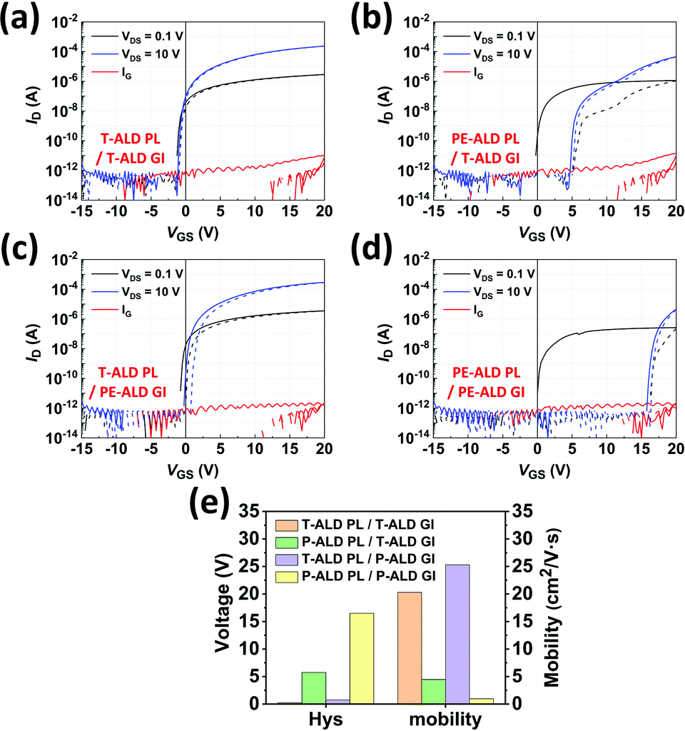 | ||
| Fig. 2 Transfer curves of a-IGZO TGBC TFTs prepared using (a) T-ALD/T-ALD, (b) PE-ALD/T-ALD, (c) T-ALD/PE-ALD, and (d) PE-ALD/PE-ALD for PL/GI Al2O3 deposition. (e) Hysteresis and linear mobility values of various a-IGZO TFTs. | ||
The delicate control of the deposition temperature of GI is a crucial factor in securing the high stability of the metal–oxide transistor.46 For more detailed optimization, we manufactured another TGBC a-IGZO TFT by changing the deposition temperature of GI to 200 °C. Hence, we fabricated a second device (device B, PL: 150 °C and GI: 200 °C) wherein the turn-on voltage was shifted by 1.14 V after the PBTS measurements, which was larger than the shift of the turn-on voltage of device A (0.35 V) [Fig. 3(a)]. According to the secondary-ion mass spectrometry (SIMS) analysis, the amounts of hydrogen and hydroxyl at the PL/GI interface were lower in device B than those in device A [Fig. 3(d and e)]. In general, ALD at a higher growth temperature lowers the amount of residual hydrogen in the films due to the complete removal of the hydroxyl groups during the surface reaction.46 However, the amount of hydrogen in the active layer/PL interface was similar for devices A and B. Because ALD-Al2O3 is an excellent hydrogen barrier,47 the temperature for the GI deposition on the top of the PL does not affect the TFT instability directly. However, in contrast to the structure of thin films for SIMS analysis, in which a-IGZO was completely covered with the Al2O3 PL, the contact between the GI of the TFT and the side edge of the exposed a-IGZO was noticeable despite the presence of the PL. Therefore, hydrogen can diffuse toward the active layer/GI interface via these contact areas to affect the reliability. These careful analyses confirmed that the increased hydrogen levels within the PL and GI were associated with improved PBTS stability. Therefore, we selected the structure of device A with good PBTS stability for fabricating monolithic oxide TFTs on the μLED array.
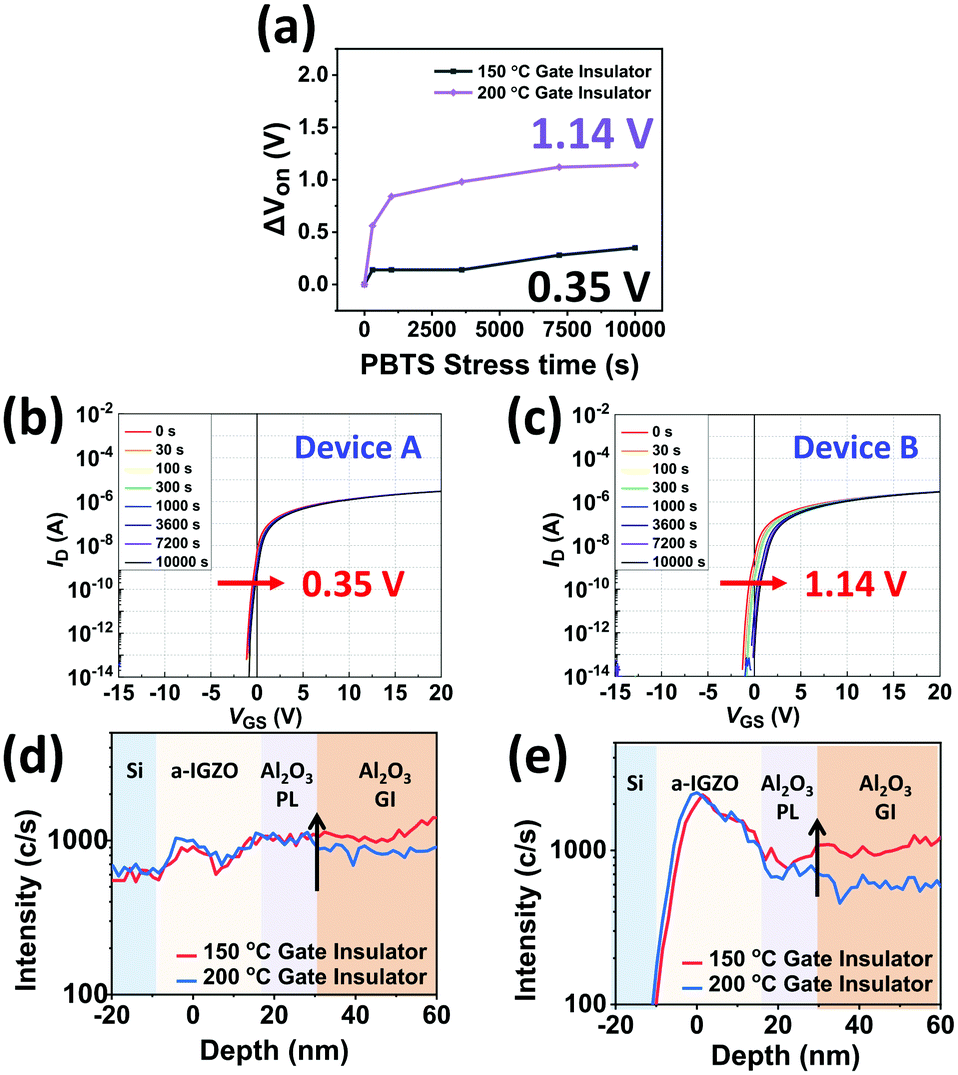 | ||
| Fig. 3 (a) Von shifts according to the GI growth temperature. PBTS stability of TGBC a-IGZO TFTs with GI Al2O3 deposited at (b) 150 °C and (c) 200 °C. (d) Hydrogen and (e) hydroxyl group peaks dictated from SIMS analysis. | ||
Before fabricating the monolithic μLEDs, we investigated the electrical properties of the a-IGZO TGBC TFTs of device A under various environments (Fig. S3, ESI†). Although the subthreshold swing, turn-on voltage, uniformity, and hysteresis values were excellent, the output characteristics showed that the drain current was not saturated at a high drain voltage. As the current saturation characteristics of TFTs have important effects on driving the μLEDs with constant luminance,48 the driving TFTs must have a saturation drain current at a specific drain voltage. In addition, the turn-on-voltage shift was −7.07 V during the NBIS stability measurements over 10000 s at −1 MV cm−1 and 0.5 mW cm−2 white light stress. Because the NBIS measurement environment corresponds to the major operation state of the μLED display,49 these unfavorable NBIS characteristics should also be addressed. Generally, the deterioration in NBIS stability originates from hydrogen impurities or ionized oxygen vacancies in metal–oxide semiconductors.47 In addition, the subgap density-of-states caused by the metal–hydrogen bonds or non-bridging oxygen hole centers can degrade the stability of NBIS.49,50 In our results, the NBTIS characteristics were poor compared to those of NBIS due to the trapping of the ionized oxygen vacancies into the defects of Al–OH or Si–OH in the gate insulator by light and thermal stress.51 Hence, to overcome these drawbacks, we inserted opaque light-blocking layers (Mo bottom gate) in the dual-gate structure.52
Fig. 4(a–d) illustrates the results of a DGBC a-IGZO TFT without applying any bottom-gate voltage, while Fig. 4(e–h) shows the corresponding results in the presence of a ground bottom-gate voltage. As shown in Fig. 4, various improved electrical properties were obtained simultaneously after a ground voltage was applied to the bottom gate. First, the ground voltage of the bottom gate rendered the turn-on voltage of the DGBC TFTs consistent regardless of the applied drain voltage [Fig. 4(a and e)]. Second, the saturated drain current was achieved, as identified from the output curves [Fig. 4(b and f)]. Third, the enhanced PBTS characteristics were also obtained; the turn-on-voltage shift during PBTS decreased from 1.16 V to 0.10 V [Fig. 4(c and g)]. These phenomena could be explained by the schematics in Fig. 4(d and h). The Von shift is caused by the electron accumulation or depletion after application of the bottom gate voltage (VBG), in which a negative VBG generates a positive shift and a positive VBG induces a negative shift [Fig. S4, ESI†].53 This shift can also be affected by introducing impurities serving as carriers, such as hydrogen. However, T-ALD Al2O3 used as the buffer oxide plays as an effective barrier, preventing impurities from entering the active interface layer. Therefore, the impact of these impurities can be effectively reduced.47 In the absence of electrical voltage with the bottom gate, the electric field caused by the drain voltage was transferred to that bottom gate. Thus, a backchannel in the a-IGZO active layer was induced close to the bottom gate. This induced backchannel can shift the turn-on voltage in a negative direction as the drain voltage increases. Furthermore, because the backchannel current can be increased as the drain voltage increases, it is difficult to gain drain saturation current characteristics in an output curve. Simultaneously, from the viewpoint of electrical stability, this backchannel surface serves as a charge trapping site at the active layer/BGI interface, thereby deteriorating the stability of PBTS.54 In contrast, when the ground voltage is applied to the bottom gate, the problems mentioned above are solved as the channel is formed only in the a-IGZO region close to TGI [Fig. 4(d and h)]. Indeed, the DGBC TFTs exhibited outstanding electrical properties, including low hysteresis, hard-saturation characteristics, and good PBTS stability, when a ground voltage was applied.
 | ||
| Fig. 4 (a and e) The transfer curve, (b and f) output curve, (c and g) PBTS stability (60 °C, 10000 s, 1 MV cm−1), and (d and h) schematics of the DGBC a-IGZO TFT in the absence and presence of a ground voltage at the bottom gate, respectively. | ||
The PBTS stability of DGBC a-IGZO TFTs was measured over 10000 s at 60 °C and 1 MV cm−1 according to the BGI deposition temperatures (150 °C, 200 °C, and 300 °C) to clarify the effect of the deposition temperature of the BGI on the electrical reliability (Fig. S5, ESI†). The amount of hydrogen in the GI can improve the PBTS stability by diffusing to the a-IGZO/GI interface. Similarly, the amount of hydrogen in the BGI positively influences the improvement of PBTS stability, supported by the SIMS data (Fig. S5, ESI†). As the deposition temperature of the BGI decreased, more amount of hydrogen was detected in the channel. Consequently, the BGI deposited at low temperatures contained more hydrogen, thereby enhancing the PBTS stability. These results suggest that our BGI films deposited at low temperatures are suitable for fabricating highly stable DGBC TFTs. Thus, high-performance DGBC TFTs can be fabricated using the Al2O3 BGI deposited at 150 °C.
To monolithically integrate the optimized DGBC TFTs on the μLED array, a thick photo-patternable insulating layer is required to planarize the pixelated μLEDs. Therefore, an organic ILD (a negative photoresist, DW-10) was introduced, which was spin-coated and patterned via conventional photolithography. Because the ILD layer can withstand temperatures up to 230 °C, the μLEDs and oxide TFTs can be sufficiently integrated at this low temperature via monolithic fabrication. In order to prevent the diffusion of hydrogen and water vapor from ILD, an extra layer of T-ALD Al2O3 buffer oxide was applied.47,55 Additional experiments were also conducted to explore the extent to which the ILD will affect the TFT performance; we deliberately omitted the ILD in the DGBC TFT structure.
Fig. S6 (ESI†) shows the TFT transfer, output curves, and stability (PBTS, NBIS, and NBTIS) of DGBC a-IGZO TFTs without the ILD layer; Fig. 5 illustrates the corresponding data for the device with the ILD layer. Comparing both results, the ILD did not degrade the TFT performance owing to the excellent barrier properties exhibited by the Al2O3 buffer layer.47 In addition, Fig. S7–S11 (ESI†) depict the uniformity of device performance within a batch and between batches. The performance of devices was found to be highly consistent among testing samples from batch to batch regardless of the device location on the substrate. These results indicate that the monolithic fabrication reported in this article shows great reproducibility and reliability. Finally, we integrated DGBC TFT arrays on μLEDs via monolithic fabrication. Fig. 6(a and b) show the subpixel layouts of the μLED and TFT arrays and the FIB-SEM images of the sub-pixel surface, respectively. Remarkably, the device fabrication proceeded as designed. In contrast to the existing inorganic ILD materials, which may contain numerous voids at low temperatures, our organic ILD (DW-10) processed by spin coating provides several merits such as rapid processability, inexpensive production cost, and no requirement for additional planarization.
 | ||
| Fig. 5 (a) Transfer curves and mobility parameters, (b) output curves, (c) PBTS stability (60 °C, 10000 s, 1 MV cm−1), (d) NBIS stability (0.5 mW cm−2 white light, 10000 s, −1 MV cm−1), and (e) NBTIS stability (60 °C, 0.5 mW cm−2 white light, 10000 s, −1 MV cm−1) of DGBC a-IGZO TFTs with an organic ILD layer between the substrate and the buffer oxide. | ||
 | ||
| Fig. 6 (a) The subpixel layouts of the μLED and DGBC TFT arrays. (b) FIB-SEM image of the surface subpixels. (c) Image of the operation of μLED and DGBC TFT arrays when both of the arrays were turned on. | ||
Fig. 6(c) illustrates an operational image of the μLED driven by DGBC TFT arrays. The scan line was swept from −15 to 20 V to ensure the proper performance of the TFT array; the data line, VDD, and VGround were 3.5, 5, and 0 V, respectively. As shown in Fig. 6(c), the phrase “KAIST 70 ppi” can be visualized, indicating that our unique methodology can achieve adequate monolithic fabrication of highly stable oxide TFTs on μLEDs under low temperature process conditions, compared to other previous achievements (Table 1). The thickness of the organic ILD on the μLEDs and unetched n-GaN was approximately 1.11 and 2.00 μm, respectively (Fig. S12, ESI†). This difference is considered reasonable as the μLED layer thickness is approximately 900 nm.
| Novelty | Driving devices | Integration method | LED | LED/driving circuit fabrication substrate | TFT structure | Bonding material | TFT process temperature | Year/ref. |
|---|---|---|---|---|---|---|---|---|
| Active-matrix (AM) driving: 8 × 8 | PMOS | Flip-chip | GaN-μLED | Sapphire/silicon | — | Solder bump | — | 2009/12 |
| High-brightness (106 cd m−2) | CMOS | Flip-chip | GaN-μLED | Sapphire/silicon | — | Bump-bonded (Au) | — | 2015/9 |
| High-brightness (40000 cd m−2), AM driving |
LTPS TFT | Flip-chip | GaN-μLED | Sapphire/glass | Conventional coplanar | Mo–Au layer | ∼450 °C | 2018/17 |
| 2D materials (transparent conducting film/channel) | Graphene FET | Monolithic with the use of the graphene transfer method | GaN-μLED | Sapphire | Bottom-gate bottom-contact | No information | No information | 2019/11 |
| Large scale (12.1 inches), full-color | LTPS TFT | Mass transfer | μLED with color conversion materials | Glass | No information | No information | ∼450 °C | 2019/19 |
| Large scale (4 inches), full-color | a-IGZO TFT | Mass transfer | μLED | Glass | Conventional coplanar | Solder bump | No information | 2020/24 |
| Real-monolithic, highly-stable TFT (also AM driving) | a-IGZO TFT | Monolithic | GaN-μLED | Sapphire | Dual-gate | Organic inter-layer dielectric | Below 230 °C | This work |
4 Conclusions
Our present study is the first to report reliable and low-temperature (below 230 °C) monolithic integration of active-matrix-μLED displays. A dual-gate a-IGZO TFT array controls the μLED displays to exhibit excellent electrical stability under the PBTS, NBIS, and NBTIS environments. In addition, this integration has been demonstrated to result in the development of superior TFTs, including reproducibility and reliability, which are crucial characteristics for future mass production in display technology. Comprehensive analyses of the electrical, structural, and chemical properties revealed that the deposited ALD-Al2O3 films had crucial roles in terms of high-quality dielectric properties and passivation of defects within the a-IGZO active layer/insulator interface by hydrogen. Our organic ILD ensures reliable interconnections by the excellent gap-filling and planarization properties, even at low temperatures, thus successfully creating the phrase “KAIST 70 ppi” from the active-matrix-μLED array. We believe that our method can be embedded in applications related to VR, AR, and biomedical sensors. Furthermore, in large-area high-resolution μLED displays, our novel monolithic method will be the cornerstone of mass production with low production costs.Author contributions
Junghoon Yang: conceptualization, data curation, formal analysis, funding acquisition, visualization, validation, writing – original draft, and writing – review and editing. HyunWoo Park: investigation, methodology, software, and writing – original draft. Baul Kim: investigation and resources, Yong-Hoon Cho: conceptualization, writing – review and editing, and supervision. Sang-Hee Ko Park: project administration, supervision, and writing – review and editing.Conflicts of interest
There are no conflicts to declare.Acknowledgements
This work was supported by the National Research Foundation of Korea (NRF) grant from the Korean Government (no. 2020R1A6A3A13061266 and 2020M3E4A1080112) and by the Industry Technology R&D Program (20006476) funded by the Ministry of Trade, Industry, and Energy (MOTIE, Korea).References
- S. Jin, J. Li, J. Li, J. Lin and H. Jiang, Appl. Phys. Lett., 2000, 76, 631–633 CrossRef CAS.
- J. Yoon, S. M. Lee, D. Kang, M. A. Meitl, C. A. Bower and J. A. Rogers, Adv. Opt. Mater., 2015, 3, 1313–1335 CrossRef CAS.
- H. E. Lee, J. H. Shin, J. H. Park, S. K. Hong, S. H. Park, S. H. Lee, J. H. Lee, I. S. Kang and K. J. Lee, Adv. Funct. Mater., 2019, 29, 1808075 CrossRef.
- Y. Huang, E.-L. Hsiang, M.-Y. Deng and S.-T. Wu, Light: Sci. Appl., 2020, 9, 1–16 CrossRef PubMed.
- E. F. Schubert and J. K. Kim, Science, 2005, 308, 1274–1278 CrossRef CAS PubMed.
- D. A. Gaul and W. S. Rees Jr, Adv. Mater., 2000, 12, 935–946 CrossRef CAS.
- L. Zhang, F. Ou, W. C. Chong, Y. Chen and Q. Li, J. Soc. Inf. Disp., 2018, 26, 137–145 CrossRef CAS.
- W. Meng, F. Xu, Z. Yu, T. Tao, L. Shao, L. Liu, T. Li, K. Wen, J. Wang and L. He, Nat. Nanotechnol., 2021, 16, 1231–1236 CrossRef CAS PubMed.
- J. Herrnsdorf, J. J. McKendry, S. Zhang, E. Xie, R. Ferreira, D. Massoubre, A. M. Zuhdi, R. K. Henderson, I. Underwood and S. Watson, IEEE Trans. Electron Devices, 2015, 62, 1918–1925 CAS.
- F. Templier, J. Soc. Inf. Disp., 2016, 24, 669–675 CrossRef CAS.
- Y. Fu, J. Sun, Z. Du, W. Guo, C. Yan, F. Xiong, L. Wang, Y. Dong, C. Xu and J. Deng, Materials, 2019, 12, 428 CrossRef CAS PubMed.
- Z. J. Liu, K. M. Wong, C. W. Keung, C. W. Tang and K. M. Lau, IEEE J. Sel. Top. Quantum Electron., 2009, 15, 1298–1302 CAS.
- E. Virey, Inf. Disp., 2018, 34, 22–27 Search PubMed.
- K. Tsuchiyama, K. Yamane, S. Utsunomiya, H. Sekiguchi, H. Okada and A. Wakahara, Appl. Phys. Express, 2016, 9, 104101 CrossRef.
- K. Myny, Nat. Electron., 2018, 1, 30–39 CrossRef CAS.
- Y. Sun, J. Fan, M. Liu, L. Zhang, B. Jiang, M. Zhang and X. Zhang, J. Soc. Inf. Disp., 2020, 28, 926–935 CrossRef CAS.
- H.-M. Kim, J. G. Um, S. Lee, D. Y. Jeong, Y. Jung, S. H. Lee, T. Jeong, J. Joo, J. Hur and J. H. Choi, Dig. Tech. Pap. - Soc. Inf. Disp. Int. Symp., 2018, 49, 880–883 CrossRef CAS.
- Z. Pan, C. Guo, X. Wang, J. Liu, R. Cao, Y. Gong, J. Wang, N. Liu, Z. Chen and L. Wang, Adv. Mater. Technol., 2020, 5, 2000549 CrossRef CAS.
- N. Sugiura, C.-T. Chuang, C.-T. Hsieh, C.-T. Wu, C.-Y. Tsai, C.-H. Lin, C.-C. Liu, C.-Y. Liu, C.-N. Yeh and C.-Y. Liu, Dig. Tech. Pap. - Soc. Inf. Disp. Int. Symp., 2019, 50, 450–453 CrossRef.
- J. F. Wager, Inf. Disp., 2014, 30, 26–29 Search PubMed.
- J. F. Wager, Inf. Disp., 2020, 36, 9–13 Search PubMed.
- H. Yabuta, M. Sano, K. Abe, T. Aiba, T. Den, H. Kumomi, K. Nomura, T. Kamiya and H. Hosono, Appl. Phys. Lett., 2006, 89, 112123 CrossRef.
- K. Nomura, H. Ohta, A. Takagi, T. Kamiya, M. Hirano and H. Hosono, Nature, 2004, 432, 488–492 CrossRef CAS PubMed.
- Y. Sun, J. Fan, B. He, M. Zhang, S. Chen, X. Zhang, C.-E. Lee and Q. Fang, A Full-Color Micro LEDs Display Based on IGZO TFT, 2020 IEEE 3rd International Conference on Electronics Technology (ICET), 2020, pp. 46–49 Search PubMed.
- K. Nomura, T. Kamiya, H. Ohta, M. Hirano and H. Hosono, Appl. Phys. Lett., 2008, 93, 192107 CrossRef.
- P. Barquinha, L. Pereira, G. Goncalves, R. Martins and E. Fortunato, Electrochem. Solid-State Lett., 2008, 11, H248 CrossRef CAS.
- A. Indluru and T. Alford, Electrochem. Solid-State Lett., 2010, 13, H464 CrossRef CAS.
- H.-W. Zan, W.-T. Chen, C.-W. Chou, C.-C. Tsai, C.-N. Huang and H.-W. Hsueh, Electrochem. Solid-State Lett., 2010, 13, H144 CrossRef CAS.
- R. Martins, D. Gaspar, M. J. Mendes, L. Pereira, J. Martins, P. Bahubalindruni, P. Barquinha and E. Fortunato, Applied Materials Today, 2018, 12, 402–414 CrossRef.
- Y. Nam, H.-O. Kim, S. H. Cho, C.-S. Hwang, T. Kim, S. Jeon and S.-H. Ko Park, J. Inf. Disp., 2016, 17, 65–71 CrossRef CAS.
- S. H. K. Park, D. H. Cho, C. S. Hwang, S. Yang, M. K. Ryu, C. W. Byun, S. M. Yoon, W. S. Cheong, K. I. Cho and J. H. Jeon, ETRI J., 2009, 31, 653–659 CrossRef.
- T. Kamiya, K. Nomura and H. Hosono, J. Disp. Technol., 2009, 5, 468–483 CAS.
- M. D. H. Chowdhury, J. G. Um and J. Jang, Appl. Phys. Lett., 2014, 105, 233504 CrossRef.
- K. Ide, K. Nomura, H. Hiramatsu, T. Kamiya and H. Hosono, J. Appl. Phys., 2012, 111, 073513 CrossRef.
- Y. Goh, J. Ahn, J. R. Lee, W. W. Park, S.-H. Ko Park and S. Jeon, ACS Appl. Mater. Interfaces, 2017, 9, 36962–36970 CrossRef CAS PubMed.
- T. Kim, J.-H. Hur and S. Jeon, Appl. Phys. Lett., 2015, 107, 093503 CrossRef.
- T. Kim, S. Park and S. Jeon, Sci. Rep., 2017, 7, 1–8 CrossRef PubMed.
- M. Powell, C. Glasse, P. Green, I. French and I. Stemp, IEEE Electron Device Lett., 2000, 21, 104–106 CAS.
- S. J. Yun, K.-H. Lee, J. Skarp, H.-R. Kim and K.-S. Nam, J. Vac. Sci. Technol., A, 1997, 15, 2993–2997 CrossRef CAS.
- J. Kim, C. Fuentes-Hernandez, W. Potscavage Jr, X.-H. Zhang and B. Kippelen, Appl. Phys. Lett., 2009, 94, 142107 CrossRef.
- H.-J. Jeong, K.-L. Han, K.-S. Jeong, S. Oh and J.-S. Park, IEEE Electron Device Lett., 2018, 39, 971–974 CAS.
- D. Kim, H. Kang, J.-M. Kim and H. Kim, Appl. Surf. Sci., 2011, 257, 3776–3779 CrossRef CAS.
- K. Ide, Y. Kikuchi, K. Nomura, M. Kimura, T. Kamiya and H. Hosono, Appl. Phys. Lett., 2011, 99, 093507 CrossRef.
- J. B. Ko, S.-H. Lee, K. W. Park and S.-H. K. Park, RSC Adv., 2019, 9, 36293–36300 RSC.
- M. S. Oh, K. Lee, J. Song, B. H. Lee, M. M. Sung, D. Hwang and S. Im, J. Electrochem. Soc., 2008, 155, H1009 CrossRef CAS.
- Y. Nam, H.-O. Kim, S. H. Cho and S.-H. K. Park, RSC Adv., 2018, 8, 5622–5628 RSC.
- Y. Kang, B. D. Ahn, J. H. Song, Y. G. Mo, H. H. Nahm, S. Han and J. K. Jeong, Adv. Electron. Mater., 2015, 1, 1400006 CrossRef.
- M. Mativenga, S. Lim, F. Haque and J. Ryu, Jpn. J. Appl. Phys., 2020, 59, 104001 CrossRef CAS.
- J. Bang, S. Matsuishi and H. Hosono, Appl. Phys. Lett., 2017, 110, 232105 CrossRef.
- K. W. Park, G. Jeon, S. Lee, J. B. Ko and S. H. K. Park, Phys. Status Solidi A, 2019, 216, 1800737 CrossRef.
- D. Kim, H. Park and B.-S. Bae, AIP Adv., 2016, 6, 035315 CrossRef.
- J. Park, C. S. Kim, Y. S. Kim, Y. C. Park, H. J. Park, B.-S. Bae, J.-S. Park and H.-S. Kim, J. Electroceram., 2016, 36, 129–134 CrossRef CAS.
- M. Chun, M. D. H. Chowdhury and J. Jang, AIP Adv., 2015, 5, 057165 CrossRef.
- J. Raja, K. Jang, H. H. Nguyen, T. T. Trinh, W. Choi and J. Yi, Curr. Appl. Phys., 2013, 13, 246–251 CrossRef.
- K.-C. Ok, S. Oh, H.-J. Jeong, J. U. Bae and J.-S. Park, IEEE Electron Device Lett., 2015, 36, 917–919 CAS.
Footnotes |
| † Electronic supplementary information (ESI) available. See DOI: https://doi.org/10.1039/d2tc01905a |
| ‡ These authors contributed equally. |
| This journal is © The Royal Society of Chemistry 2022 |