
Structural engineering of single-crystal-like perovskite nanocrystals for ultrasensitive photodetector applications†
Mi Kyong
Kim
a,
Zumuukhorol
Munkhsaikhan
b,
Se Gyo
Han
c,
Su Min
Park
b,
Haedam
Jin
a,
Jeongbeom
Cha
a,
Seok Joo
Yang
c,
Jungyoon
Seo
d,
Hwa Sung
Lee
 *d,
Chel-Jong
Choi
*b and
Min
Kim
*ab
*d,
Chel-Jong
Choi
*b and
Min
Kim
*ab
aGraduate School of Integrated Energy-AI, Jeonbuk National University, Jeonju, 54896, Republic of Korea. E-mail: minkim@jbnu.ac.kr
bSchool of Semiconductor and Chemical Engineering, Clean Energy Research Center, Jeonbuk National University, Jeonju, 54896, Republic of Korea. E-mail: cjchoi@jbnu.ac.kr
cDepartment of Chemical Engineering, Pohang University of Science and Technology, Pohang, 37673, Republic of Korea
dDepartment of Materials Science and Chemical Engineering, Hanyang University, Ansan, 15588, Republic of Korea. E-mail: hslee78@hanyang.ac.kr
First published on 21st July 2022
Abstract
Nanostructured organic–inorganic hybrid perovskite materials have attracted much attention due to their excellent performance in optoelectronics and facile solution-processability compared with their bulk and thin-film counterparts. Herein, we successfully synthesized well-defined one-dimensional single-crystalline perovskite nanomaterials for the application of photodetectors (PDs). We controlled synthesis parameters, such as reaction time and mechanical agitations, to deviate crystal structures into quantum dots, nanowires, and nanorods, which are studied comparatively and related to their optoelectrical properties. In particular, we demonstrate that the perovskite nanorods are structured with single-crystal-like molecular orientation, which significantly enhances PD performances compared to nanowires and quantum dots. We constructed PDs using the perovskite nanorods that exhibited excellent photodetection performance with a responsivity of 40 A W−1, external quantum efficiency of 1.3 × 10⁴%, and detectivity of 3.3 × 10¹⁴ Jones, respectively, with exceptional device stability over one-month storage.
Introduction
Photodetectors (PDs) have attracted widespread attention in the past few decades, owing to their compelling applications in optical communication devices, image sensing equipment, wearable electronics, industrial automation, environmental monitoring, biological agent detection, medical instruments, space exploration, and missile warning systems.1–6 The photo-detecting functional unit is considered as one of the crucial components in the development of advanced, high-performance PDs.7,8 Metal halide perovskites have been identified as a promising material in the optoelectronics field due to their tunable bandgap, high and well-balanced electron/hole mobilities, long carrier diffusion length, and solution processability.9–11 The excellent optoelectrical property of perovskite materials makes them a promising material to use for photodetector devices.Perovskite materials have been tailored to form either polycrystalline thin films or colloidal quantum dots (QDs) using antisolvent dripping crystallization, hot-injection method, ligand-assisted reprecipitation method, and mechanical grinding crystallization.12 Perovskite QDs possess several advantages over polycrystalline thin films, some of which include widely tunable bandgap energy, efficient photoluminescent quantum yield, and low charge recombination at grain boundaries.13 In addition, one of the advantages of perovskite QDs is their wide adaptability to solution processing without complex post-treatments after QDs have been synthesized. QDs, however, are limited in size to a few tens of nanometers, which can lead to shorter charge transport lengths than crystalline thin films.10,14,15
Compared to QDs, the building blocks of low-dimensional nanostructures (e.g., nanowires, nanorods, nanobelts, and single-crystal structures) have drawn attraction in the development of novel and efficient optoelectronics, and it is due to their high crystallinity, mechanical flexibility, and efficient photoelectric characteristics. Especially, nanowires with confined width also exhibit the quantum confinement effect, which enables easier bandgap tuning, a lower recombination rate, and an extended carrier lifetime.1,16–18 Charge carriers in 1D nanocrystals can move efficiently along the longitudinal direction of nanowires without passing crystal grain boundaries, which makes 1D materials more suitable for use than QDs in high-performance photodetector applications.1,4,19–21 Although nanowires have few grain boundaries along the crystal growth direction, their charge transport property is not as efficient as that of single-crystals. Furthermore, single crystals have drawbacks for processability due to their tedious synthesis method and poor printability. Only a few studies have examined the fabrication of highly crystalline low-dimensional perovskite nanomaterials using the solution process.
In this study, we report a method of synthesizing highly crystalline one-dimensional (1D) perovskite nanomaterials for use in photodetector applications. We modified the hot-injection method to fabricate 1D single-crystal-like perovskite nanorods (NRs) in a solution phase. We compared the crystalline structure of NRs with other nanocrystal shapes of QDs and nanowires (NWs).22,23 We investigated the overall crystalline structure of the NRs using X-ray diffraction and transmission electron microscopy (TEM) and correlated it with electrical properties by measuring spectral response and external quantum efficiency. The NRs-based photodetector device exhibited the highest responsivity and response time levels compared to NWs and QDs systems. The photodetector devices were tested over fifty days to analyze their air durability. The results of our experiment provide a method of synthesizing high-quality perovskite nanocrystals with efficient optoelectronic properties that are relevant for the fabrication of perovskite-based 1D nanomaterials to be used in a wide range of optoelectronic applications.
Results and discussion
We synthesized CsPbBr3 nanomaterials based on a modified hot-injection method under a nitrogen and vacuum environment (Fig. 1).22,23 Perovskite nanomaterials were fabricated by injecting Cs-oleate precursor solution into a reaction vessel containing PbBr2, ligands, and a non-coordinating solvent. Various studies have developed to structurally control nanocrystals in multi-dimensional shapes by adjusting the synthesis methods and adopting short-length ligands.9,17,24–28 Especially, the chemical structure of ligand molecules and their varied combinations influenced the growth directions of perovskite crystals.29 While conventional ligand molecules, including oleic acid and oleylamine, lead to the formation of quantum dots (QDs),22,30 the mixed ligand molecules, including octylamine and oleylamine, induce anisotropic growth of perovskite nanowires (NWs).23–25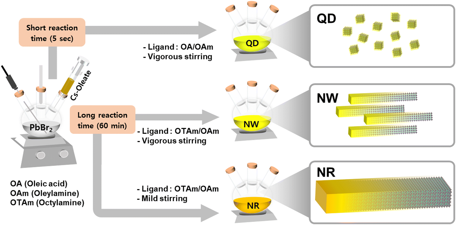 | ||
| Fig. 1 Schematic illustration of the synthesis process for the CsPbBr3 QDs, NWs, and NRs. | ||
To synthesize single-crystalline 1D nanomaterials, we manipulated the reaction conditions related to mechanical agitations, which could change the growth mechanism of perovskite nanocrystals from NWs to nanorods (NRs). The degree of aggregation of nanomaterials can be regulated via kinetic control, such as the degree of mechanical agitation of atomic agents.31,32 We controlled stirring conditions with respect to the batch size to facilitate the aggregation of crystal seeds, which leads to the aggregation of primary nanoparticles into more extensive superstructures. Under weak agitation and weak shear flow, the primary nanowires aggregated via side-to-side packing into superstructures that resulted in the formation of highly crystalline nanorod particles, which can be explained by the Ostwald ripening mechanism.33–35 X-Ray photoelectron spectroscopy confirmed that CsPbBr3 QDs, NWs, and NRs had identical binding energies in the desired chemical compositions (Fig. S1, ESI†).
To analyze the crystal shape and structure of the synthesized CsPbBr3 nanomaterials, TEM and SEM images were obtained (Fig. 2). The TEM image of QDs exhibits standard cubic crystals with average sizes of ∼12.06 ± 1.93 nm (Fig. 2a). The SEM image of the spincoated QDs film shows that the QDs formed island-structured aggregates on the substrate (Fig. 2d). The TEM image of the NWs displays a uniformly-defined one-dimensional structure (width ∼ 10.99 ± 1.35 nm, length > 10 μm) with an ultrahigh aspect ratio over 1000 (Fig. 2b). The SEM image of the spin-cast NWs film displays that they are likely to aggregate, forming closely packed wire aggregates (Fig. 2e). On the other hand, the TEM and SEM images of NRs show enlarged 1D crystals with an average width of 148 nm and length over a few μm (Fig. 2c and f). The TEM image exhibiting the NRs mixed with NWs demonstrates that the formation of NR is driven by the Ostwald ripening mechanism, which was supported by the lattice-matched aggregation of NWs (Fig. S2, ESI†).34,35 The HRTEM image of the QDs shows that the d-spacing in the (100) planes in the cubic phase was 5.8 Å (Fig. 2g). The HRTEM images of NWs and NRs display that the 1D growth of crystals are in the direction of (100) crystalline planes with a perfect lattice-matching manner.
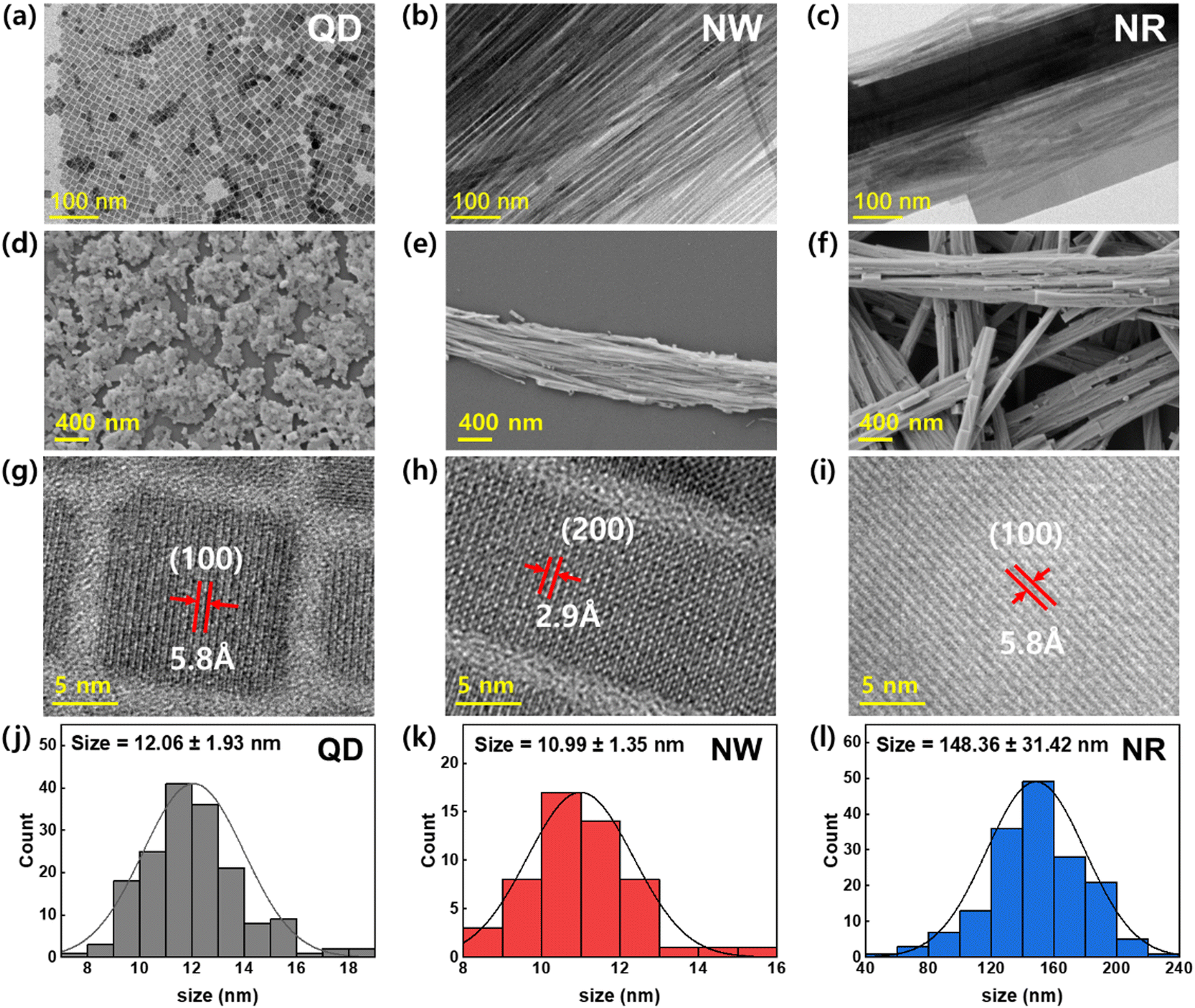 | ||
| Fig. 2 TEM images of the CsPbBr3 (a) QDs, (b) NWs, and (c) NRs. SEM images of the CsPbBr3 (d) QDs, (e) NWs, and (f) NRs. HRTEM images with lattice fringes of the CsPbBr3 (g) QDs, (h) NWs, and (i) NRs. Crystal size distribution histogram of the CsPbBr3 (j) QDs, (k) NWs, and (l) NRs. | ||
The XRD patterns of CsPbBr3 QDs, NWs, and NRs were obtained to investigate their crystal structure (Fig. 3). The XRD profiles of the QDs and NWs films indicate that the QDs and NWs are composed of a crystal structure of cubic phase (Fig. 3a and b). Conversely, the XRD profile of the NRs film shows a sharp difference compared to the QD and NW films (Fig. 3c). The dominant scattering peaks of (100) and (200) planes remained; however, other scattering peaks became negligible. These results confirm that the NRs were oriented epitaxially with a single-crystal-like alignment, in agreement with the HRTEM images.36 The 2D XRD image of the QDs film exhibits the characteristic Debye ring scattering pattern of all diffraction peaks with random orientations of QDs (Fig. 3d).36 In the case of NWs, the XRD image shows Debye ring patterns at the diffraction peaks, but with strengthened intensities along the qz-axis (Fig. 3e). The strengthened intensity can be explained by the NWs, having a high aspect ratio, were geometrically limited to assemble randomly opposed to the QDs.36 On the other hand, the 2D XRD pattern of the NRs exhibits spotty diffraction patterns at characteristic scattering peaks at (100) and (200) planes (Fig. 3f). This indicates that the NRs retained a long-range ordered crystalline phase similar to a single-crystal orientation.36,37
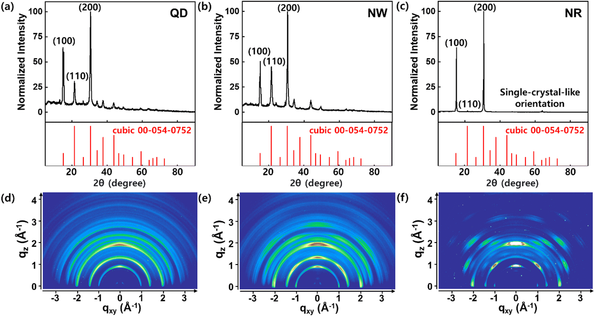 | ||
| Fig. 3 XRD patterns of the CsPbBr3 (a) QDs, (b) NWs, and (c) NRs with standard XRD reference (cubic: PDF 00-054-0752). 2D XRD patterns of the CsPbBr3 (d) QDs, (e) NWs, and (f) NRs. | ||
We analyzed the optical properties of the synthesized nanocrystals (Fig. 4). Fig. 4a shows the UV-vis absorbance of QDs, NWs, and NRs in a solution state. The absorption spectrum exhibited excitonic peaks centered at 501 nm, 517 nm, and 525 nm in QDs, NWs, and NRs, respectively. NWs and NRs demonstrated background scattering above the absorption edge due to a strong light scattering effect between the assemblies of aggregates formed in a solution state. The PL spectra analysis of the nanomaterials showed peaks located at 524 nm for QDs, 524 nm for NWs, and 534 nm for NRs (Fig. 4b). We confirmed that the PL peaks of QDs and NWs were identical, which indicates that the strong quantum confinement effect in QDs similarly applies to NWs because the width of the NWs was similar to the size of the QDs.18
 | ||
| Fig. 4 (a) Optical absorption spectrum of the CsPbBr3 QDs, NWs, and NRs. (b) PL spectra of the CsPbBr3 QDs, NWs, and NRs. (c) Time-resolved PL decay of the CsPbBr3 QDs, NWs, and NRs with the bi-exponential fitting models. | ||
As shown in Fig. 4c, a time-resolved PL (TRPL) analysis measured the photogenerated carrier lifetime. The average lifetimes in the QDs, NWs, and NRs films were measured to be 4.49 ns, 8.74 ns, and 13.3 ns, respectively, according to the calculation from the bi-exponential decay model (Table 1)
 | (1) |
 | (2) |
| CsPbBr3 | A 1 (%) | τ 1 (ns) | A 2 (%) | τ 2 (ns) | τ av (ns) |
|---|---|---|---|---|---|
| QDs | 83.0 | 1.12 | 17.0 | 7.09 | 4.49 |
| NWs | 79.6 | 1.84 | 20.4 | 12.7 | 8.74 |
| NRs | 60.8 | 3.05 | 39.2 | 16.3 | 13.3 |
To investigate the optoelectronic performance of the perovskite nanomaterials, we fabricated photodetector devices featuring a metal–semiconductor–metal-type structure (Fig. 5). The perovskite nanomaterials were deposited on silicon wafers with pre-patterned Au interdigitated electrodes by spin coating (Fig. 5a). The SEM images of the fabricated devices show that the nanomaterials, including QDs, NWs, and NRs, were connected by a bridge between two electrodes with a gap of 5 μm. The photoresponse characteristics of the photodetector devices were measured under the illumination of a wavelength of 405 nm at −3 V bias.
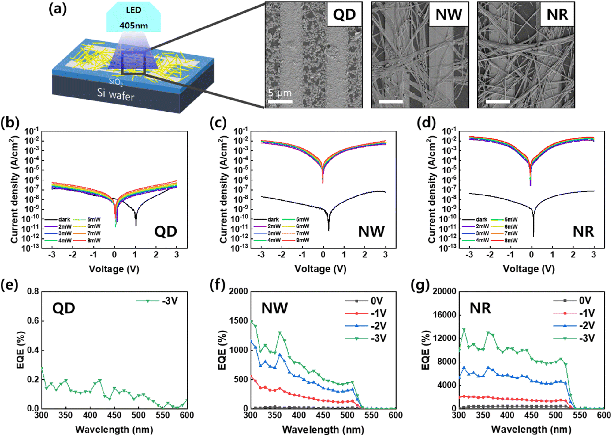 | ||
| Fig. 5 (a) Schematic illustration of the constructed photodetector device and SEM images of the nanomaterials based on the CsPbBr3 QDs, NWs, and NRs. J–V characteristics of the photodetectors under different illumination intensities based on the CsPbBr3 (b) QDs, (c) NWs, and (d) NRs. EQE spectra of the photodetectors at various bias voltages based on the CsPbBr3 (e) QDs, (f) NWs, and (g) NRs. | ||
The current density–voltage (J–V) curves of the PD devices in the dark and under illumination with light intensity varied from 0 mW to 8 mW. In the darkness, the three devices exhibited a similar current density ranging from 10–100 nA cm−2. The CsPbBr3 perovskites act as p-type semiconductors, and the PD devices in this architecture operate in a mode of conductor type, in which photogenerated holes transport in the direction of the applied external field while electrons are trapped in the active area.1–5,7,38 The holes transporting toward the opposite electrode recombine with electrons drawn from the external circuit. In this device operation, large photoconductive can be gained if high mobility or a short pathway between the electrodes is fulfilled.
The QDs-PD showed a weak photoconductive gain compared to dark current (Fig. 5b). The minimum current point of the QDs-PD shifts close to 1 V, which originated from a strong charge trapping property with the formation of the space charge region in the channel (Fig. S4, ESI†). The SEM image of the QDs exhibit that QDs hardly construct a connection network between two electrodes due to their small size and island-like film formation (Fig. 5a). Conversely, the light J–V curves for the NWs-PD and NRs-PD increased significantly with light intensities reaching 10–100 mA cm−2 (Fig. 5c and d). The calculated on/off ratios were 105–106 for the NWs-PD and NRs-PD. The photocurrent's dependence on light intensity is examined in the ESI,† which a power law can describe: I–Pθ; where P is light intensity, and θ is the exponent (Fig. S5, ESI†).39 The θ of 0.47 was obtained by fitting the light intensity versus photocurrent curve, which was in agreement with previous results that reported high crystalline perovskite nanocrystal with a relatively low density of defect states.6,39,40
Fig. 5e–g show the photoresponsivity of the PD devices under illumination with wavelengths ranging from 300 to 600 nm. In order to examine the wavelength-dependent responsivity (R), responsivity and external quantum efficiency (EQE) were calculated using the following equations:
 | (3) |
 | (4) |
![[thin space (1/6-em)]](https://www.rsc.org/images/entities/char_2009.gif) 000%, respectively, with wavelengths from 300 to 520 nm, which was correlated with the optical analysis.
000%, respectively, with wavelengths from 300 to 520 nm, which was correlated with the optical analysis.
The magnitude of the EQE was dependent on the photogeneration rate of charge carriers and charge extraction efficiency.1 The efficient charge transport through NWs and NRs accelerated hole injection by elevating energy levels under illumination. This led to high EQE values of over 1000% due to photomultiplication.4,41,42 The J–V curve and EQE analysis confirmed that the charge transport was more efficient in the NRs-PD compared to the NWs-PD. The responsivity of the NWs-PD was calculated to be 4 A W−1, and that of the NRs-PD was calculated to be 40 A W−1 (Fig. S6, ESI†).
To investigate the dynamic photodetector response, we measured the −3 dB bandwidth, which was obtained from the plots of the normalized response versus frequency analysis (Fig. 6).43 The −3 dB cut-off frequency of the NWs-PD and NRs-PD were determined to be 90 and 250 Hz, respectively (Fig. 6a and b). Fig. 6c and d show the responses to temporal square-shaped wave signals at a frequency of 4 Hz. The trise and tdecay of the NRs-PD were 49.0 ms and 33.0 ms, respectively, which were faster than the NWs-PD (trise = 59.8 ms, tdecay = 41.5 ms). We concluded that the NRs-PD was more efficient than the NWs-PD device not only in terms of responsivity but also the response speed.
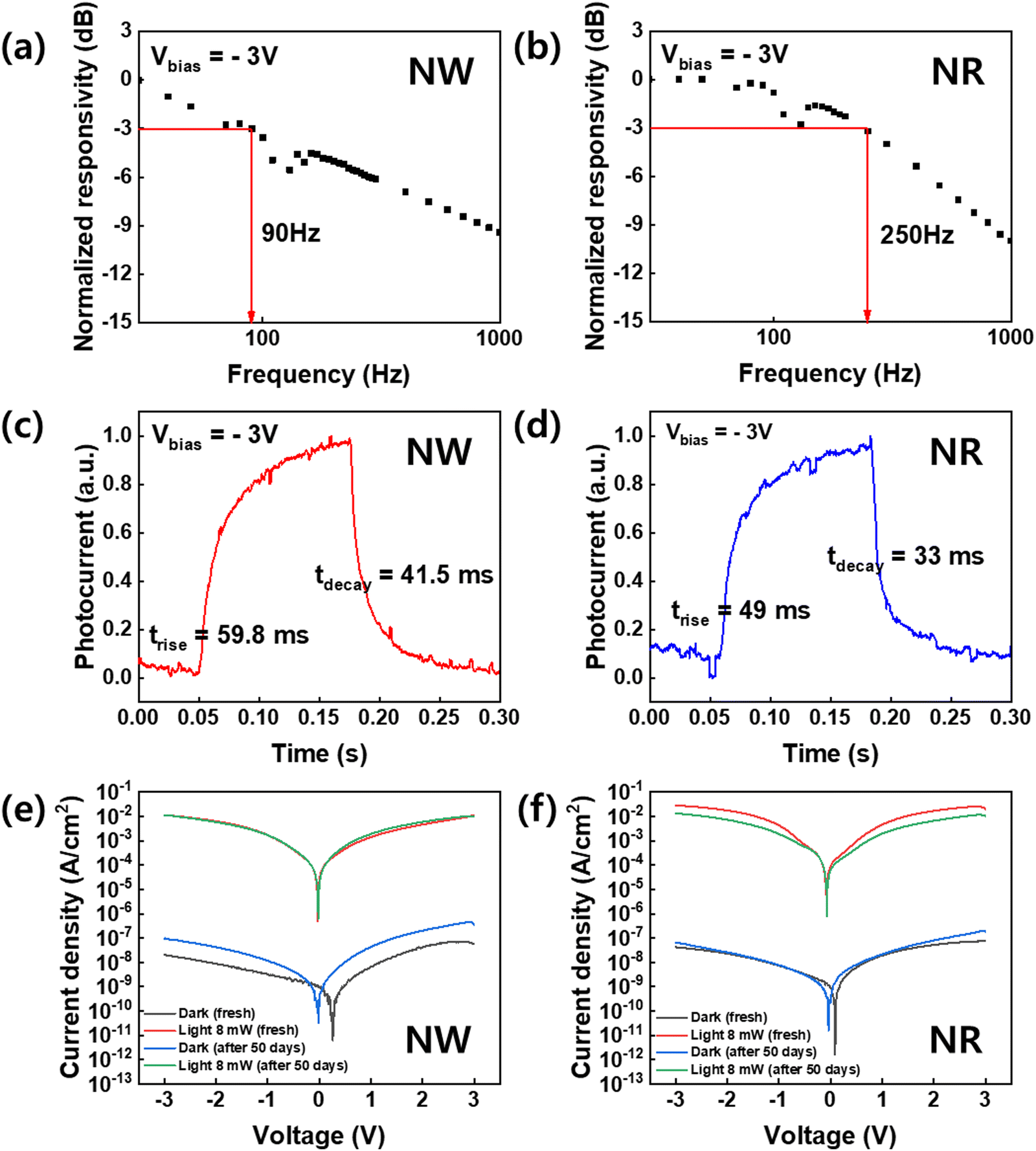 | ||
| Fig. 6 Frequency responses of the CsPbBr3 (a) NWs and (b) NRs photodetectors. The temporal photocurrent responses a pulse frequency of 4 Hz based on the photodetector of the CsPbBr3 (c) NWs and (d) NRs. The dark and light J–V characteristics of the photodetectors based on the CsPbBr3 (e) NWs and (f) NRs as pristine and after 50 days. | ||
The air durability of the perovskite NWs and NRs-fabricated devices was tested under 405 nm illumination at room temperature over fifty days (Fig. 6e and f). Under −3 V bias, the photocurrents of the NWs-PD and the NRs-PD were 0.01 and 0.05 A cm−2 in their pristine state, which did not change significantly after fifty days. This indicates that the crystalline property of the perovskite NWs and NRs did not significantly degrade in air at room temperature and maintained excellent photodetector performance. We also measured the XRD of NWs and NRs after long-term storage of 9 months, which exhibits that NWs degrade mostly into PbBr2 and Cs4PbBr6 phase while NRs barely change their pristine XRD patterns of the cubic perovskite phase (Fig. S7, ESI†). This degradation was only observed as phase transitions without morphological change (Fig. S8, ESI†).
Detectivity (D*), an important parameter for photodetectors, was calculated using the equation
 | (5) |
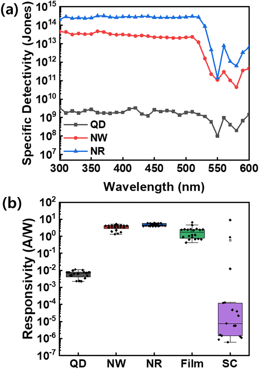 | ||
| Fig. 7 (a) Specific detectivity of the CsPbBr3 QDs, NWs, and NRs photodetectors at −3 V. (b) Responsivity of the CsPbBr3 QDs, NWs, NRs, thin-film, and single crystals (SCs) photodetectors. | ||
| Device type | Perovskite morphology | Bias [V] | R [A W−1] | D* [Jones] | EQE [%] | On/off ratio | τ rise/τdecay [ms] | Ref. |
|---|---|---|---|---|---|---|---|---|
| Photoconductor | QDs | −3 | 7 × 10⁻⁴ | 3.4 × 10⁹ | 0.28 | 5 | — | This work |
| Photoconductor | NWs | −3 | 4 | 4.7 × 10¹³ | 1498 | 5.6 × 10⁵ | 59.8/41.5 | This work |
| Photoconductor | NRs | −3 | 40 | 3.3 × 10¹⁴ | 13609 |
6.7 × 10⁵ | 49/33 | This work |
| Photoconductor | QDs | 2 | 20 | 8.9 × 10¹³ | — | 1 × 10⁵ | 4700/2300 | 51 |
| Photoconductor | Microparticles | 10 | 0.18 | 6.1 × 10¹⁰ | 41 | 8 × 10³ | 1.8/1.0 | 47 |
| Photoconductor | Microcrystals | 3 | 6 × 10⁴ | 1 × 10¹³ | 2 × 10⁷ | — | 0.5/1.6 | 57 |
| Photoconductor | Microcrystals | 0 | 0.173 | 4.8 × 10¹² | — | 1.3 × 10⁵ | 0.14/0.12 | 55 |
| Photoconductor | Single NW | 1 | 4 × 10³ | — | — | — | 0.252/0.3 | 19 |
| Photodiode | NWs | 0 | 0.3 | 1 × 10¹³ | — | 1 × 10⁶ | 0.4/0.43 | 54 |
| Photoconductor | NWs | — | — | — | — | 1 × 10³ | — | 23 |
| Photoconductor | NWs | 6 | — | — | — | 1 × 10³ | 82/54 | 56 |
| Photoconductor | NW network | 5 | — | — | — | 1 × 10³ | 100 | 58 |
| Photoconductor | NW arrays | — | 1380 | — | — | 1 × 10³ | 0.0215/0.0234 | 45 |
| Photoconductor | Microwires | 5 | 118 | 8 × 10¹² | 2 × 10⁷ | 1 × 10² | 38/36 | 50 |
| Photoconductor | NSs | 10 | 0.64 | — | 54 | 1 × 10⁴ | 0.019/0.024 | 53 |
| Phototransistor | NSs | 1 | — | — | — | 1 × 10² | 17.8/15.2 | 46 |
| Photoconductor | Nanoplates | 1.5 | 34 | 7.5 × 10¹² | 1 × 10⁴ | 1 × 10³ | 0.6/0.9 | 52 |
| Photoconductor | Micro/nanoflakes | 5 | 2.776 | — | 1250 | 1 × 10² | 40/20 | 44 |
| Photoconductor | Microplatelets | 5 | 1.33 | 8.9 × 10¹¹ | 407 | 4.6 × 10³ | 20.9/24.6 | 48 |
| Photoconductor | Thin film | 6 | 55 | 9 × 10¹² | 16700 |
1 × 10⁵ | 0.43/0.318 | 49 |
| Photoconductor | Thin film | 15 | — | — | — | 1.5 × 10⁴ | 233/213 | 59 |
| Photoconductor | Single crystal | 6 | 2.1 | — | — | 4.6 × 10² | 300/300 | 60 |
| Photoconductor | Single crystal | 5 | 0.028 | 1.8 × 10¹¹ | 7 | 1 × 10² | 90.7/57.0 | 61 |
To demonstrate the efficient and reliable PD performance of NRs, we compared various perovskite-based PDs in terms of device statistics, including QDs, NWs, NRs, bulk thin film, and single-crystals (SCs) based on the identical CsPbBr3 perovskites (Fig. 7b, Fig. S9 and S10, ESI†). The box plots of responsivities exhibit that the NRs-PD has the narrowest and highest responsivity distribution of ∼20 measured devices among the nanocrystals, thin-film, and SCs. Especially, the thin-film-based PD and single-crystal-based PD devices show dispersive device statistics due to the grain boundary for thin films and the difficulty in SCs device fabrication; however, the NR materials secure the device reproducibility and reliable processability. The results of our study confirm that the NRs-based device has excellent detection abilities and holds great potential for development as a reliable photodetector.
Conclusion
In conclusion, we report the synthesis of CsPbBr3 perovskite QDs, NWs, and NRs using a modified hot injection method for photodetector applications. We produced NRs with controlled synthesis conditions to facilitate crystal aggregations, which led to a lattice-matching single-crystal orientation of the NRs. The geometric features of the fabricated NWs and NRs, including connected networks between parallel electrodes, are advantageous for photoconductive-type photodetector applications. The manufactured photodetector with NRs achieved a maximum EQE of 13600%, along with light responsivity of 40 A W−1 and a specific detectivity of 3.3 × 10¹⁴ Jones. The device possessed a fast photodetector response with −3dB width at 250 Hz, and a high Ilight/Idark ratio of over 105. The NRs-PD device's performance was confirmed to be superior to those of previously studied photodetectors composed of CsPbBr3 materials. The low-cost and facile synthesis method provides a novel manner of synthesizing all-inorganic single-crystal-like NRs and preparing high-performance 1D perovskite optoelectronic devices. We believe that the results obtained in this study can be used to develop perovskite nanocrystal-based photodetectors for use in numerous applications.
Experimental details
Materials
Cesium carbonate (Cs2CO3, 99.995%, Sigma-Aldrich), lead bromide (PbBr2, 98%, TCI), cesium bromide (CsBr, 99.999%, Alfa Aesar), 1-octadecene (ODE, 90%, Alfa Aesar), hexane (anhydrous, 95%, Sigma-Aldrich), toluene (anhydrous, 99.8%, Sigma-Aldrich) octane (anhydrous, 99%, Sigma-Aldrich), methanol (CH3OH, anhydrous, 99.8%, Sigma-Aldrich), dimethyl formamide (DMSO, anhydrous, 99.9%, Sigma-Aldrich), N,N-dimethylformamide (DMF, anhydrous, 99.8%, Sigma-Aldrich), dichloromethane (DCM, ACS reagent, 99.5%, Sigma-Aldrich), ethyl acetate (anhydrous, 99.8%, Sigma-Aldrich), and methyl acetate (anhydrous, 99.5%, Sigma-Aldrich) were used as received without further purification. Oleic acid (OA, 90%, Sigma-Aldrich), oleylamine (OAm, 70%, Sigma-Aldrich), and octylamine (OTAm, 99%, Sigma-Aldrich) were dehydrated before use.Synthesis of CsPbBr3 nanocrystals
Preparation of CsPbBr3 thin films
CsPbBr3 thin films were fabricated through two-step deposition method.59 Firstly, CsBr (30 mg) was dissolved in methanol (2 mL) in a heated sealed container at 50 °C for 30 min and PbBr2 (734 mg) in DMF (2 mL) was stirred by a hot plate at 75 °C for 1 h. The solution was subsequently filtered by a PTFE filter (0.2 μm pore size). The PbBr2 precursor solution was spin-coated at 3000 rpm for 30 s, followed by drying on a hotplate at 75 °C for 15 min. After being baked, the sample was put into the CsBr solution in methanol at 55 °C for 15 min. The following annealing procedure was taking at 70 °C for 24 h.Synthesis of CsPbBr3 single crystals
CsPbBr3 single crystals were grown with the slow diffusion of vapor of the anti-solvent DCM into the precursor solution.60 First, CsBr (0.127 g) and PbBr2 (0.539 g) were dissolved in DMSO (3 mL) under ultra-sonication until no precipitation was observed. To prevent inhomogeneous crystallization, the precursor solution was filtered with a PTFE filter (0.2 μm pore size). The clear solution was poured into a 20 mL glass vial and the vial was stored in a 500 mL glass container under a DCM atmosphere at room temperature. After sitting overnight, crystal seeds formed, which slowly grew up to the millimeter size at the bottom of the vial over 3–4 days.Device fabrication
A substrate of Si and SiO2 layers was used, and Ti/Au were deposited using a photolithographic process. The width and spacing of the electrode fingers were 5 μm. A photodetector was fabricated by spin coating the nanocrystal solutions, containing the CsPbBr3 QDs, NWs, and NRs in octane at 40 mg mL−1. The perovskite solution was spin coated at 1500 rpm for 60 s. Then, methyl acetate was spin-coated at 4000 rpm for 10 seconds to wash ligands. The above-mentioned entire spin-coating process was repeated twice.Characterization
High-resolution transmission electron microscope (HRTEM) images were taken (JEOL, JEM-2010) at an accelerating voltage of 200 kV. The field-emission electron scanning microscope (FESEM) images were also taken (Carl Zeiss, Gemini500) at an accelerating voltage of 2 kV. The HRTEM and FESEM images were obtained at the Center for University-Wide Research Facilities of Jeonbuk National University (South Korea). High-resolution X-ray diffractometer (HRXRD) patterns were recorded with a Bruker D8 Advance Diffractometer with a Cu Kα source. UV-Vis absorption spectra were measured with a UV-vis spectrophotometer (V-670, JASCO). Photoluminescence spectra were measured with a JASCO FP-6500 spectrofluorometer. Time-resolved photoluminescence (TRPL) and photoluminescence quantum yield (PLQY) were analyzed using a HORIBA Fluorolog3 spectrofluorometer at the Future Energy Convergence Core Center (FECC). X-Ray photoelectron spectroscopy was measured with a Theta Probe (Thermo Fisher Scientific, UK) at the Jeonju location of the Korea Basic Science Institute (KBSI). J–V characteristics were measured with an Agilent 4155A semiconductor parameter analyzer using a 405 nm LED. The active area of PD device was 0.006324 cm2. EQE spectra were measured using a photomodulation spectroscopy setup under modulated monochromatic light at 45 Hz. Illumination was provided using a light source composed of a 500 W Hg (Xe) arc lamp and an optical chopper. Photocurrents were measured using a Stanford Research SR-570 low-noise current preamplifier and a Stanford Research SR-830 lock-in amplifier. The −3 dB cut-off frequency was measured using the SR-830 with a 532nm LED modulated by a 33500B Series Waveform Generator (Keysight). Temporal rise time and decay time were measured using a TDC3054C digital oscilloscope (Tektronix) that was equipped with a modulated LED.Author contributions
M. K. conceived the idea, designed the experiments and performed data analysis. Z. M. and S. G. H. measured the fabricated devices and photophysical characterization. S. M. P. and H. J. synthesized thin films and single crystals for device characterizations. J. C., S. J. Y., and J. S. conducted GIWAXS analysis. H. S. L., C.-J. C. and M. K. wrote the manuscript and gave guidance for this study. All authors discussed the results and commented on the manuscript.Conflicts of interest
The authors state that there are no conflicts to declare.Acknowledgements
This work was supported by a grant from the National Research Foundation of Korea (NRF) funded by the Korean government (MSIT) (No. 2021R1C1C1012188). The authors would like to thank the Writing Center at Jeonbuk National University for its skilled proofreading service.References
- H. P. Wang, S. Li, X. Liu, Z. Shi, X. Fang and J. H. He, Adv. Mater., 2021, 33, e2003309 CrossRef PubMed.
- C. Li, Y. Ma, Y. Xiao, L. Shen and L. Ding, InfoMat, 2020, 2, 1247–1256 CrossRef CAS.
- S. Cai, X. Xu, W. Yang, J. Chen and X. Fang, Adv. Mater., 2019, 31, e1808138 CrossRef PubMed.
- H. Gu, S. C. Chen and Q. Zheng, Adv. Opt. Mater., 2020, 9, 2001637 CrossRef.
- Y. Zhang, Y. Ma, Y. Wang, X. Zhang, C. Zuo, L. Shen and L. Ding, Adv. Mater., 2021, 33, e2006691 CrossRef PubMed.
- L. H. Zeng, Q. M. Chen, Z. X. Zhang, D. Wu, H. Yuan, Y. Y. Li, W. Qarony, S. P. Lau, L. B. Luo and Y. H. Tsang, Adv. Sci., 2019, 6, 1901134 CrossRef CAS PubMed.
- Y. Dong, Y. Zou, J. Song, X. Song and H. Zeng, J. Mater. Chem. C, 2017, 5, 11369–11394 RSC.
- F. Wang, X. Zou, M. Xu, H. Wang, H. Wang, H. Guo, J. Guo, P. Wang, M. Peng, Z. Wang, Y. Wang, J. Miao, F. Chen, J. Wang, X. Chen, A. Pan, C. Shan, L. Liao and W. Hu, Adv. Sci., 2021, 8, 2100569 CrossRef CAS PubMed.
- J. Shamsi, A. S. Urban, M. Imran, L. De Trizio and L. Manna, Chem. Rev., 2019, 119, 3296–3348 CrossRef CAS PubMed.
- L. Protesescu, S. Yakunin, M. I. Bodnarchuk, F. Krieg, R. Caputo, C. H. Hendon, R. X. Yang, A. Walsh and M. V. Kovalenko, Nano Lett., 2015, 15, 3692–3696 CrossRef CAS PubMed.
- Y. Tong, B. J. Bohn, E. Bladt, K. Wang, P. Muller-Buschbaum, S. Bals, A. S. Urban, L. Polavarapu and J. Feldmann, Angew. Chem., Int. Ed., 2017, 56, 13887–13892 CrossRef CAS PubMed.
- D. Chen and X. Chen, J. Mater. Chem. C, 2019, 7, 1413–1446 RSC.
- L. Liu, A. Najar, K. Wang, M. Du and S. F. Liu, Adv. Sci., 2022, 9, e2104577 CrossRef PubMed.
- J. Chen, D. Jia, E. M. J. Johansson, A. Hagfeldt and X. Zhang, Energy Environ. Sci., 2021, 14, 224–261 RSC.
- J. Yuan, A. Hazarika, Q. Zhao, X. Ling, T. Moot, W. Ma and J. M. Luther, Joule, 2020, 4, 1160–1185 CrossRef CAS.
- L. N. Quan, J. Kang, C. Z. Ning and P. Yang, Chem. Rev., 2019, 119, 9153–9169 CrossRef CAS PubMed.
- C. Zhang, J. Chen, S. Wang, L. Kong, S. W. Lewis, X. Yang, A. L. Rogach and G. Jia, Adv. Mater., 2020, 32, e2002736 CrossRef PubMed.
- M. Imran, F. Di Stasio, Z. Dang, C. Canale, A. H. Khan, J. Shamsi, R. Brescia, M. Prato and L. Manna, Chem. Mater., 2016, 28, 6450–6454 CrossRef CAS PubMed.
- M. Shoaib, X. Zhang, X. Wang, H. Zhou, T. Xu, X. Wang, X. Hu, H. Liu, X. Fan, W. Zheng, T. Yang, S. Yang, Q. Zhang, X. Zhu, L. Sun and A. Pan, J. Am. Chem. Soc., 2017, 139, 15592–15595 CrossRef CAS PubMed.
- Y. Li, Z. Shi, L. Lei, Z. Ma, F. Zhang, S. Li, D. Wu, T. Xu, X. Li, C. Shan and G. Du, ACS Photonics, 2018, 5, 2524–2532 CrossRef CAS.
- S. Li, Y. Li, Z. Shi, L. Lei, H. Ji, D. Wu, T. Xu, X. Li and G. Du, Sol. Energy Mater. Sol. Cells, 2019, 191, 275–282 CrossRef CAS.
- C. Lu, M. W. Wright, X. Ma, H. Li, D. S. Itanze, J. A. Carter, C. A. Hewitt, G. L. Donati, D. L. Carroll, P. M. Lundin and S. M. Geyer, Chem. Mater., 2018, 31, 62–67 CrossRef.
- D. Zhang, Y. Yang, Y. Bekenstein, Y. Yu, N. A. Gibson, A. B. Wong, S. W. Eaton, N. Kornienko, Q. Kong, M. Lai, A. P. Alivisatos, S. R. Leone and P. Yang, J. Am. Chem. Soc., 2016, 138, 7236–7239 CrossRef CAS PubMed.
- K. Chen, Q. Zhong, W. Chen, B. Sang, Y. Wang, T. Yang, Y. Liu, Y. Zhang and H. Zhang, Adv. Funct. Mater., 2019, 29, 1900991 CrossRef.
- M. Yu, D. Zhang, Y. Xu, J. Lin, C. Yu, Y. Fang, Z. Liu, Z. Guo, C. Tang and Y. Huang, J. Colloid Interface Sci., 2022, 608, 2367–2376 CrossRef CAS PubMed.
- Q. Zhong, M. Cao, Y. Xu, P. Li, Y. Zhang, H. Hu, D. Yang, Y. Xu, L. Wang, Y. Li, X. Zhang and Q. Zhang, Nano Lett., 2019, 19, 4151–4157 CrossRef CAS PubMed.
- L. Ruan, W. Shen, A. Wang, Q. Zhou, H. Zhang and Z. Deng, Nanoscale, 2017, 9, 7252–7259 RSC.
- F. Haydous, J. M. Gardner and U. B. Cappel, J. Mater. Chem. A, 2021, 9, 23419–23443 RSC.
- M. A. Boles, D. Ling, T. Hyeon and D. V. Talapin, Nat. Mater., 2016, 15, 141–153 CrossRef CAS PubMed.
- T. Udayabhaskararao, M. Kazes, L. Houben, H. Lin and D. Oron, Chem. Mater., 2017, 29, 1302–1308 CrossRef CAS.
- M. Manteghian and S. Ghader, Chem. Eng. Technol., 2009, 32, 835–839 CrossRef CAS.
- R. Valenzuela, M. C. Fuentes, C. Parra, J. Baeza, N. Duran, S. K. Sharma, M. Knobel and J. Freer, J. Alloys Compd., 2009, 488, 227–231 CrossRef CAS.
- H. Lee, J. Park, H. Cho, J. Lee and K.-H. Lee, RSC Adv., 2021, 11, 38152–38160 RSC.
- H. Huang, J. Raith, S. V. Kershaw, S. Kalytchuk, O. Tomanec, L. Jing, A. S. Susha, R. Zboril and A. L. Rogach, Nat. Commun., 2017, 8, 996 CrossRef PubMed.
- G. Almeida, L. Goldoni, Q. Akkerman, Z. Dang, A. H. Khan, S. Marras, I. Moreels and L. Manna, ACS Nano, 2018, 12, 1704–1711 CrossRef CAS PubMed.
- N. Widjonarko, Coatings, 2016, 6, 54 CrossRef.
- J. Wang, S. Luo, Y. Lin, Y. Chen, Y. Deng, Z. Li, K. Meng, G. Chen, T. Huang, S. Xiao, H. Huang, C. Zhou, L. Ding, J. He, J. Huang and Y. Yuan, Nat. Commun., 2020, 11, 582 CrossRef CAS PubMed.
- X. Huang, Y. Guo and Y. Liu, Chem. Commun., 2021, 57, 11429–11442 RSC.
- K. Shen, X. Li, H. Xu, M. Wang, X. Dai, J. Guo, T. Zhang, S. Li, G. Zou, K.-L. Choy, I. P. Parkin, Z. Guo, H. Liu and J. Wu, J. Mater. Chem. A, 2019, 7, 6134–6142 RSC.
- H. Fang, J. Li, J. Ding, Y. Sun, Q. Li, J. L. Sun, L. Wang and Q. Yan, ACS Appl. Mater. Interfaces, 2017, 9, 10921–10928 CrossRef CAS PubMed.
- R. Dong, Y. Fang, J. Chae, J. Dai, Z. Xiao, Q. Dong, Y. Yuan, A. Centrone, X. C. Zeng and J. Huang, Adv. Mater., 2015, 27, 1912–1918 CrossRef CAS PubMed.
- F. Mei, D. Sun, S. Mei, J. Feng, Y. Zhou, J. Xu and X. Xiao, Adv. Phys.: X, 2019, 4, 1592709 CAS.
- M. Zhang, F. Zhang, Y. Wang, L. Zhu, Y. Hu, Z. Lou, Y. Hou and F. Teng, Sci. Rep., 2018, 8, 11157 CrossRef PubMed.
- W. Zheng, X. Xiong, R. Lin, Z. Zhang, C. Xu and F. Huang, ACS Appl. Mater. Interfaces, 2018, 10, 1865–1870 CrossRef CAS PubMed.
- J. Feng, X. Yan, Y. Liu, H. Gao, Y. Wu, B. Su and L. Jiang, Adv. Mater., 2017, 29, 1605993 CrossRef PubMed.
- L. Lv, Y. Xu, H. Fang, W. Luo, F. Xu, L. Liu, B. Wang, X. Zhang, D. Yang, W. Hu and A. Dong, Nanoscale, 2016, 8, 13589–13596 RSC.
- X. Li, D. Yu, F. Cao, Y. Gu, Y. Wei, Y. Wu, J. Song and H. Zeng, Adv. Funct. Mater., 2016, 26, 5903–5912 CrossRef CAS.
- Y. Li, Z. Shi, L. Lei, F. Zhang, Z. Ma, D. Wu, T. Xu, Y. Tian, Y. Zhang, G. Du, C. Shan and X. Li, Chem. Mater., 2018, 30, 6744–6755 CrossRef CAS.
- Y. Li, Z.-F. Shi, S. Li, L.-Z. Lei, H.-F. Ji, D. Wu, T.-T. Xu, Y.-T. Tian and X.-J. Li, J. Mater. Chem. C, 2017, 5, 8355–8360 RSC.
- P. Gui, Z. Chen, B. Li, F. Yao, X. Zheng, Q. Lin and G. Fang, ACS Photonics, 2018, 5, 2113–2119 CrossRef CAS.
- L. Zhou, K. Yu, F. Yang, H. Cong, N. Wang, J. Zheng, Y. Zuo, C. Li, B. Cheng and Q. Wang, J. Mater. Chem. C, 2017, 5, 6224–6233 RSC.
- X. Liu, D. Yu, F. Cao, X. Li, J. Ji, J. Chen, X. Song and H. Zeng, Small, 2017, 13, 1700364 CrossRef PubMed.
- J. Song, L. Xu, J. Li, J. Xue, Y. Dong, X. Li and H. Zeng, Adv. Mater., 2016, 28, 4861–4869 CrossRef CAS PubMed.
- H. Zhou, Z. Song, C. R. Grice, C. Chen, J. Zhang, Y. Zhu, R. Liu, H. Wang and Y. Yan, Nano Energy, 2018, 53, 880–886 CrossRef CAS.
- H. Zhou, J. Zeng, Z. Song, C. R. Grice, C. Chen, Z. Song, D. Zhao, H. Wang and Y. Yan, J. Phys. Chem. Lett., 2018, 9, 2043–2048 CrossRef CAS PubMed.
- W. Zhai, J. Lin, C. Li, S. Hu, Y. Huang, C. Yu, Z. Wen, Z. Liu, Y. Fang and C. Tang, Nanoscale, 2018, 10, 21451–21458 RSC.
- B. Yang, F. Zhang, J. Chen, S. Yang, X. Xia, T. Pullerits, W. Deng and K. Han, Adv. Mater., 2017, 29, 1703758 CrossRef PubMed.
- J. Chen, Y. Fu, L. Samad, L. Dang, Y. Zhao, S. Shen, L. Guo and S. Jin, Nano Lett., 2017, 17, 460–466 CrossRef CAS PubMed.
- R. Chen, Z. Liang, W. Feng, X. Hu and A. Hao, J. Alloys Compd., 2021, 864, 158125 CrossRef CAS.
- J. H. Cha, J. H. Han, W. Yin, C. Park, Y. Park, T. K. Ahn, J. H. Cho and D. Y. Jung, J. Phys. Chem. Lett., 2017, 8, 565–570 CrossRef CAS PubMed.
- J. Ding, S. Du, Z. Zuo, Y. Zhao, H. Cui and X. Zhan, J. Phys. Chem. C, 2017, 121, 4917–4923 CrossRef CAS.
Footnote |
| † Electronic supplementary information (ESI) available. See DOI: https://doi.org/10.1039/d2tc01854c |
| This journal is © The Royal Society of Chemistry 2022 |