
 Open Access Article
 This Open Access Article is licensed under a
 Creative Commons Attribution 3.0 Unported Licence
Color controllable smart white lighting based on various device architectures of electrically driven quantum-dot light-emitting diodes†
Dong-Wook
Shin‡
 ,
Sanghyo
Lee‡
,
Hyung Woo
Choi
,
Sang Yun
Bang
,
Soo Deok
Han
,
Yul Jae
Cho
,
Xiang-Bing
Fan
,
Jeong-Wan
Jo
,
Limeng
Ni
,
Chatura
Samarakoon
,
Adrees
Arbab
,
Jiajie
Yang
,
Yoonwoo
Kim
,
Sung-Min
Jung
*,
Luigi G.
Occhipinti
,
Gehan A. J.
Amaratunga
and
Jong Min
Kim
*
,
Sanghyo
Lee‡
,
Hyung Woo
Choi
,
Sang Yun
Bang
,
Soo Deok
Han
,
Yul Jae
Cho
,
Xiang-Bing
Fan
,
Jeong-Wan
Jo
,
Limeng
Ni
,
Chatura
Samarakoon
,
Adrees
Arbab
,
Jiajie
Yang
,
Yoonwoo
Kim
,
Sung-Min
Jung
*,
Luigi G.
Occhipinti
,
Gehan A. J.
Amaratunga
and
Jong Min
Kim
*
Electrical Engineering Division, Department of Engineering, University of Cambridge, 9 JJ Thomson Avenue, CB3 0FA, UK. E-mail: sj569@cam.ac.uk; jmk71@cam.ac.uk
First published on 29th June 2022
Abstract
A comprehensive study of the various device architectures of patterned-, stacked-, and mixed-type quantum-dot light-emitting diodes (QD-LEDs) for smart white lighting has been performed by way of computational simulation and experimental device fabrication. The layout of the patterned-type QD-LED has been optimized by a rigorous charge transport simulation and a numerical grid searching color optimization method. The patterned-type QD-LED devices are fabricated using a unique transfer printing technique to validate design concepts. The architectural dependency on the color of the stacked-type QD-LED has been computationally and experimentally explored by the charge transport simulation with the electric-field-dependent carrier hopping model and by fabricating the devices with a multi-step spin-coating process. The mixed-type QD-LED has also been experimentally analyzed by the QD volume mixing ratios in the mixture solution. These three types of patterned, stacked, and mixed QD-LED device architectures show potential for various applications of functionalized next-generation smart white lighting systems.
1. Introduction
Lighting devices are used in multiple contexts for the daily life of human beings such as general illumination, automotive, communication, imaging, and healthcare.1–5 Situated in many ambient positions of crucial importance, they consume 19% of the world's energy.6 The industry of smart lighting as part of the smart home system has grown for more than a decade, and the current research trends on smart lighting systems have been focused on the improvement of energy efficiency so far.7 The smart lighting system with an adjustable color temperature with a flexible shape has also been studied in order to maximize the aesthetic and psychological effects of the lighting on human beings.8 According to the personal preference on the emotional perception of light for different color temperatures, reddish-white light with a lower color temperature is favored in the case of indoor conditions either early in the morning or in the evening, while bluish-white light with a higher color temperature is suitable in the day bright time.9–11To achieve the controllability of the color temperature for the smart lighting system, various light-emitting diodes (LEDs) have been widely studied.12–16 Among the various materials for LED devices, quantum dots (QDs), which are inorganic materials, are capable of higher color purity, narrow bandwidth, high quantum yield, photo/thermal stability, and easily tunable bandgap.17–21 Electroluminescent (EL) quantum-dot light-emitting diodes (QD-LEDs) show high brightness owing to the stability of inorganic materials for the high current density. Furthermore, since the device structure of QD-LEDs is quite similar to the organic LEDs (OLEDs) of the thin planar structure, QD-LEDs also have a form factor of surface lighting with flexible shapes. Therefore, ultimate smart lighting devices with high color capability and artistic design can be realized through EL-based QD-LEDs with high brightness, color tunability, sharpness of the color spectrum and flexible form factors.22–25
The device architectures of QD-LEDs for white lighting are classified as mixed, stacked, and patterned types, where the emissive layers (EMLs) of the devices are formed by different configurations of QDs. In the patterned-type QD-LEDs, each of the red (R), green (G), and blue (B) QD emission areas is pixelated in a stripe pattern at different locations to form an EML. In the case of the stacked-type QD-LED, the EML is a multi-layered structure that consists of heterogeneous QD layers. The EML of the mixed-type QD-LED is a compounded layer in which R, G, and B QD nanoparticles are mixed and randomly located. The patterned-type QD-LED is fabricated by patterning spatially separated R, G and B subpixels via a transfer printing process.26,27 The stacked-type QD-LED is fabricated via a multi-step spin-coating process by stacking vertically the R, G and B QD layers.28,29 The mixed-type is fabricated via a single-step spin-coating process by simply mixing R, G, and B QDs in the solution.26,30,31
To date, individual studies have been performed separately for each type of device architecture to enhance their electro-optical performances. Moreover, most of them are focused on optimizing the lighting properties of the devices in experimental ways with limited strategies of device design. These experimental approaches not only demand huge time and effort but also result in inaccurate performance prediction on target specifications. To precisely design the lighting properties of the QD-LED based white lighting, one of the systematic and efficient approaches is to analyse the electro-optical properties by the computational simulation of charge transport models for the given device architectures. However, few ideas of computational design and analysis have been established up to now due to the lack of a complete simulation model in QD-LED devices.32,33
In this research, we perform a comprehensive analysis and optimization of the electro-optical properties of the patterned-, stacked-, and mixed-types of EL-based QD-LED device architectures for smart white lighting. First, the lighting properties of the patterned-type QD-LEDs are optimized by designing the layout of the pixelated patterns of R, G, and B QD-LEDs with a rigorous computational charge transport simulation model. The electro-optical characteristics of the patterned-type QD-LED and its color behaviors for the applied voltage are quantitatively predicted by the charge transport simulation combined with the color simulation. To validate the design concept from the computational simulation, the device having the optimized layout is fabricated using a unique transfer printing technique. Next, the electro-optical properties of the stacked-type QD-LEDs are experimentally analyzed by fabricating the R/G/B and B/G/R sequential QD stacks via the solution process of multi-step spin-coating. In particular, the computational modelling of the heterogeneous QD layers is attempted through the complete charge transport model with the electric-field-dependent carrier hopping process, to theoretically explain the experimental color behaviors depending on the stack sequence of QD layers. Finally, the electro-optical properties including the chromaticity and its variation of the mixed-type QD-LEDs are experimentally analyzed by fabricating the devices via the single-step spin-coating process for various combinations of R, G, and B QD volume mixing ratios in the solution mixture. The electro-optical properties such as chromaticity difference, CCT, luminance and current density with respect to the applied voltage and the external quantum efficiency (EQE) for the luminance are discussed. For the fabrication and simulation of each type of QD-LED device, cadmium selenide (CdSe) and zinc sulfide (ZnS) core/shell QD nanoparticles are used in this study.
Throughout the comprehensive study, the electro-optical properties of three different types of QD-LEDs for white lighting are summarized to discuss their potential applications for a next-generation smart lighting system according to their lighting characteristics. These three types of QD-LEDs show their unique spectral controllability for a white lighting device, which makes precise color tuning for advanced smart lighting systems.
2. Results and discussion
2.1 Architectures of the white lighting device and charge transport model in QD-LEDs
Fig. 1 shows the device structure of QD-LEDs used in this study for the white lighting system. A QD-LED device consists of a stack of a hole injection layer (HIL), a hole transport layer (HTL), an EML, and an electron transport layer (ETL) sandwiched between anode and cathode electrodes (Fig. 1a). The thicknesses of the ETL, HTL, and HIL are measured to be 20 nm, 20 nm, and 20 nm, respectively, by transmission electron microscopy (TEM) analysis (Fig. S1, ESI†). The flat-band energy-levels of each material along the z-axis are plotted in Fig. 1b. Poly(3,4-ethylenedioxythiophene)-poly(styrenesulfonate) (PEDOT:PSS), poly[(9,9-dioctylfluorenyl-2,7-diyl)-co-(4,4′-(N-(4-sec-butylphenyl)diphenylamine)] (TFB), and magnesium-doped zinc oxide (MZO) are used as the HIL, HTL, and ETL, respectively. Indium tin oxide (ITO) and aluminum (Al) are used as the cathode and the anode, respectively. CdSe and ZnS are used as the core and shell materials of QDs for the EML layer. The material parameters of the transport layers are listed in Table S1 (ESI†). | ||
| Fig. 1 Schematic illustration of the device structures and configuration used for the simulation of a white lighting system with different types of QD-LEDs. (a) Device architecture of QD-LEDs used in this study. The device is configured with stratified layers of an anode, an HIL, an HTL, an EML, an ETL, and a cathode electrode on a glass substrate. (b) Flat-band energy-level diagram across the device with respect to the distance z from the anode/HIL interface. TFB and MZO are used as HTL and ETL materials, and the CdSe/ZnS core/shell QDs are used as the EML in this study. (c) Configuration of pixelated QDs in the EML of patterned-type QD-LEDs. Light having different peak wavelengths is emitted separately from each of the pixelated QD patterns. (d) Layer configuration of stacked QDs in the EML of the stacked-type QD-LEDs. The QDs are stacked sequentially in the order of R/G/B as an example and light having different peak wavelengths is emitted separately from each of the QD layers. (e) Random arrangement of QD nanoparticles in the EML of the mixed-type QD-LEDs. The QDs are randomly positioned in the EML due to the coating process with a mixture solution of R, G, B QDs and light having different peak wavelengths is emitted from each of the QDs. | ||
Since the structure of the QD-LED device is a stack of very thin multiple layers (Fig. 1a), the device structure can be assumed to be a form of an infinite slab, where the emission properties are invariant to the direction parallel to the device plane (xy-plane). Therefore, a one-dimensional charge transport model is developed to simulate the carrier density and electric-field distributions along the z-axis (ESI†). The schematic pathways for possible current flow across the QD-LED devices are also depicted in Fig. 1b. The charge transport across the device can be described by (i) drift-diffusion current densities Jdp and Jdn in the HIL/HTL and ETL, (ii) hopping current densities Jhp and Jhn between two neighboring QD layers, and (iii) injection current densities Jip and Jin between the QD layer and charge transport layers.32,33 First, the HIL, HTL and ETL can be considered ordinary semiconductors where the charge transport can be explained by the band transport with the drift-diffusion process. Next, for the charge injection current at the interfaces between the QD layer and the HTL or ETL, holes and electrons are injected into the QD layer after a certain threshold voltage that carriers overcome the band offset, according to the electric field-dependent charge capturing process. Finally, for the hopping current, the electric field-dependent charge capturing process together with the Boltzmann tunnelling process is considered to include the energy-level difference and the electric-field effect between QDs (ESI†).
The white light can be obtained by configuring the R, G, and B QDs in the single EML of the QD-LED device by means of various fabrication methods. The device architectures of the possible QD arrangements for the white lighting are patterned-, stacked-, and mixed-type QD-LEDs schematically illustrated in Fig. 1c–e. To obtain the emission spectrum for white lighting with wide color variation, device architectures with an appropriate QD combination and composition should be optimally designed. Here, the Commission Internationale de l’Eclairage (CIE) D65 standard illuminant having a correlated color temperature (CCT) of 6500 K is used as a target illuminant for the color design of the QD-LED based white lighting device.34 By tuning the emission contributions of each QD species to the entire emission spectrum according to their own design factors of patterned-, stacked-, and mixed-type QD-LEDs, the chromaticity close to the CIE D65 illuminant can be obtained.
The QD arrangement in the EML of the patterned-type QD-LED is illustrated in Fig. 1c. Each of the QD stripe patterns is pixelated at different locations with its emission width. The patterned-type QD-LED is fabricated by the transfer printing technology (ESI†).27,28 The QD patterns are sandwiched by the same transport layers and electrodes, simultaneously, and hence the same driving voltage is applied to each pattern at the same time. The simplest way to control the emission contribution of each QDs to the entire emission spectrum is to design the emission widths of the QD patterns. The major design factors of the patterned-type QD-LED are the widths of the stripe patterns for each emission area of QDs to achieve the chromaticity of the D65 illuminant at a specific voltage.
Fig. 1d shows an example illustration of the stacked-type QD-LED in which different species of QD layers are staked onto the HTL surface in the order of R, G, and B (denoted by ‘R/G/B’). The stacked-type QD-LED can be mainly designed by the stack order and the thickness of QD layers. Here, the thickness of the QD layer can be determined by the QD solution concentration and the spin-speed in the solution spin-coating process. Each of the R, G, and B QD layers emit lights according to their accumulation of holes and electrons depending on their stack configuration and layer conditions. For the three species of R, G, and B QD layers, six combinations of the stack sequences are possible. Among the six stack combinations, R/G/B and B/G/R stack sequences which are the only ascending and descending orders of optical bandgaps have been selected in this study to examine the bandgap arrangement effect on the charge transport in the stacked-type QD-LED devices. The color properties of the R/G/B and B/G/R stack sequences with the different QD solution concentrations are analyzed experimentally by means of device fabrication. In particular, to explain the experimental color behaviors depending on the stack sequences, the computational modelling of the heterogeneous QD layers of the R/G/B and B/G/R stacks in the EML is attempted through the complete charge transport model with the electric-field-dependent carrier hopping process (ESI†).
Fig. 1e shows the device architecture and the arrangement of the QDs in the mixed-type QD-LED device. The mixed-type QD-LED has an EML with randomly distributed R, G, and B QDs on the HTL. The randomized QD layer is formed by a solution process with a solution mixture of R, G, and B QDs according to their QD concentrations in the solution (ESI†). Owing to the randomized arrangement of QDs, a mixture of light can be emitted from random locations in the EML of the lighting system. To obtain the desired white light, the major design factors are the solution concentrations of each R, G, and B QDs determining their emission contributions to the entire emission spectrum. In this study, the experimental electro-optical properties including the color behaviors are analyzed by means of device fabrication under various combinations of the QD solution concentrations.
2.2 Architecture of the patterned-type QD-LED based white lighting device
The first approach to achieving white light with multiple species of QDs is a patterned-type QD-LED which consists of multiple stripe-patterned QDs pixelated in a single device. To achieve the chromaticity of the CIE D65 illuminant, the major design factors of the device layout are pattern widths of the QD emission area. To design the emission widths of QDs, the intrinsic spectral radiances of the monochromatic R, G, and B QD-LEDs with respect to the applied voltage should be obtained first. In this study, the intrinsic spectral radiances of the R, G, and B QD-LED devices are simulated by the charge transport model. To simulate the actual device, the device and material parameters are obtained experimentally by transmission electron microscopy (TEM) analysis and by the fabrication of individual monochromatic devices.
Fig. 2a–c show the TEM images of R, G, and B QD (CdSe/ZnS core/shell) particles used for the fabrication and simulation of the devices. From the TEM analysis, the particle sizes of the R, G, and B QDs are assumed to be 15.0 nm, 8.5 nm, and 7.0 nm, respectively. With the given QDs, monochromatic R, G, and B QD-LED devices are fabricated by the transfer printing technology. Insets show the snapshots of the fabricated EL-driven monochromatic R, G, and B QD-LEDs having device sizes of 3.0 × 1.5 mm2, and their CIE color coordinates are displayed in Fig. S2a (ESI†). Fig. 2d–f show the experimental luminance L, current density J, and EQE of the fabricated devices with respect to voltage and current density. In Fig. 2d, the R, G, and B QD-LED devices show luminance values of 11![[thin space (1/6-em)]](https://www.rsc.org/images/entities/char_2009.gif) 340 cd m−2, 30150 cd m−2, and 1405 cd m−2 at 7 V, respectively. All the luminance values on a logarithmic scale increase abruptly just after a threshold voltage defined at a luminance of 1 cd m−2. The threshold voltages of the R, G, and B QD-LED devices were observed to be 1.8 V, 2.6 V, and 3.6 V, and the maximum EQEs were also measured to be 7.2%, 2.3%, and 1.0% at 3.4 V, 4.8 V, and 5.4 V, respectively (Fig. 2e). The current densities at the maximum EQE are measured to be 0.015 A cm−2, 0.059 A cm−2, and 0.067 A cm−2, for the respective devices (Fig. 2f). For the given particle sizes, the material parameters of QDs were appropriately chosen for the simulated EQE curves to match the experimental EQE curves. The material parameters of QDs used in the simulation are listed in Table S2 (ESI†).
340 cd m−2, 30150 cd m−2, and 1405 cd m−2 at 7 V, respectively. All the luminance values on a logarithmic scale increase abruptly just after a threshold voltage defined at a luminance of 1 cd m−2. The threshold voltages of the R, G, and B QD-LED devices were observed to be 1.8 V, 2.6 V, and 3.6 V, and the maximum EQEs were also measured to be 7.2%, 2.3%, and 1.0% at 3.4 V, 4.8 V, and 5.4 V, respectively (Fig. 2e). The current densities at the maximum EQE are measured to be 0.015 A cm−2, 0.059 A cm−2, and 0.067 A cm−2, for the respective devices (Fig. 2f). For the given particle sizes, the material parameters of QDs were appropriately chosen for the simulated EQE curves to match the experimental EQE curves. The material parameters of QDs used in the simulation are listed in Table S2 (ESI†).
 | ||
| Fig. 2 Electro-optical properties of the fabricated and simulated monochromatic R, G, and B QD-LEDs. TEM images of CdSe/ZnS QD nanoparticles of (a) R, (b) G, and (c) B QDs. Insets are the snapshots of the fabricated EL-driven monochromatic R, G, and B QD-LED devices having emission sizes of 3.0 × 1.5 mm2. (d) Experimental current densities J and luminance L of the fabricated R, G, and B QD-LED devices for the applied voltage. Experimental EQEs for R, G, and B QD-LED devices for (e) the applied voltage and (f) the current density. Simulated hole and electron densities around the QD layers of (g) R, (h) G, and (i) B QD-LEDs for the distance from the anode/HIL interface. (j) Simulated current densities and luminance of the fabricated R, G, and B QD-LEDs for the applied voltage. Simulated EQEs for R, G, and B QD-LEDs for (k) the applied voltage and (l) the current density. | ||
Fig. 2g–i show the simulated hole and electron density distributions p and n near the QD layers of R, G, and B QD-LED devices for different applied voltages. Here, for the one-dimensional charge transport simulation, it is assumed that two QD layers are vertically stacked in the EML, as observed by TEM analysis in Fig. S1 (ESI†). The peak wavelengths of the R, G, and B QDs are set to be 620 nm, 558 nm, and 450 nm, respectively, for the photoluminescence (PL) spectra of the QDs used for the device fabrication in Fig. S2b (ESI†). The holes and electrons accumulated at the boundaries of the HTL and ETL are injected after a certain threshold voltage due to the electric-field-dependent carrier capturing process. The carrier densities at the QDs abruptly increase as the voltage increases after the threshold voltage. The R QD-LED shows less accumulation of charge carriers at QD layers compared to the G and B QD-LEDs due to the weakest electric field caused by its largest QD diameter. The flat-band energy-level diagram, simulated electric potential distributions, energy distributions, and electric field distributions for the respective devices are plotted in Fig. S3 (ESI†). The simulated hole and electron densities accumulated at the QD layer, pQD and nQD, and the radiative recombination rates per unit area, RRAD, with respect to the applied voltage are also plotted in Fig. S4 (ESI†).
Fig. 2j–l show the simulated voltage-dependences of current density, luminance, and EQE of the monochromatic R, G, and B QD-LED devices. The luminance values of the R, G, and B QD-LEDs at 7 V were simulated to be 9709 cd m−2, 27523 cd m−2, and 529 cd m−2, respectively (Fig. 2j). The threshold voltages of the simulated R, G, and B QD-LED devices were 2.1 V, 2.7 V, and 4.0 V which are slightly higher values than the experimental threshold voltages. In Fig. 2k and l, the simulated EQE curves of all the R, G, and B QD-LEDs with respect to the applied voltage and the current density coincide very well with the experimental EQE curves. Therefore, it is expected that our charge transport simulation model can reliably predict the emission spectra of the monochromatic devices for the following layout design of the patterned-type QD-LED device.
Fig. 3a shows the device architecture of the patterned-type QD-LED configured by stripe-pattered R, G and B QD subpixels with their emission widths wR, wG, and wB. Here, the pitch of the pixel group is denoted by P, and the weighting factors of the respective subpixels denoted by aR, aG, and aB are defined by an = wn/P for n ∈ {R, G, B}, and hence the sum of the weighting factors is always equal to 1. Since the photons emitted from each QD pattern are independent and do not affect each other due to the structural feature of the patterned-type white QD-LED, the total emission spectrum of the patterned-type QD-LED can be expressed by the linear combination of the individual emission spectrum of each R, G, and B QD pattern without any loss. With the given weighting factors of the pixel layout, the emission spectrum L(λ, Va) of the EL-driven patterned-type QD-LED for a given applied voltage Va can be obtained using eqn (1).
| L(λ, Va) = aRSR(λ, λR, Va) + aGSG(λ, λG, Va) + aBSB(λ, λB, Va) | (1) |
 | ||
| Fig. 3 Optimization of lighting properties by designing the layout of the patterned-type QD-LEDs. (a) Device structure of the patterned-type QD-LEDs. (b) Simulated spectral radiances of the monochromatic R, G, and B QD-LED devices at different applied voltages. (c) Grid searching method to find the optimal weighting factors for a minimum chromaticity difference. Simulated spectral radiances of (d) reference device with identical emission weighting factors and (e) optimized device with different emission weighting factors at different voltages. Insets are the pixel layouts of the two patterned-type QD-LEDs. (f) Simulated color loci of the reference and optimized devices for the applied voltage. Experimental spectral radiances of the fabricated (g) reference and (h) optimized devices at different voltages. Insets are the snapshots of the EL-driven patterned-type QD-LED devices of reference and optimized devices. (i) Experimental color loci of the reference and optimized devices for the applied voltage. (j) Chromaticity difference and CCT of the optimized device for the applied voltage. (k) Experimental current and luminance curves of the optimized device for the applied voltage. (l) Experimental EQE curve of the optimized devices for the applied voltage. | ||
Once the total emission spectrum of the patterned-type QD-LED is calculated, the chromaticity difference of the device at a given voltage is calculated using eqn (2),
| Δxy = |CIExy(L(λ, Va)) − CIExy(D65(λ))|, | (2) |
For comparison of the color performance, the voltage-dependent spectrum of the simulated patterned-type QD-LED device with identical weighting factors aR = aG = aB of 1/3 (inset layout) is plotted in Fig. 3d as a reference device. The simulated spectral radiance of the reference device shows the identical spectral distribution to the summation of the spectral distribution of the monochromatic devices with three times smaller peak radiances. The voltage-dependent spectrum of the simulated device with different weighting factors (inset layout) optimized by the grid searching method is also plotted in Fig. 3e. Here, at 5 V, the red peak is suppressed, and the blue peak is enhanced compared to the spectrum of the reference device owing to the optimized weighting factors. After 5 V, the peak radiance of blue emission is dramatically enhanced as the voltage increases owing to the enlarged emission area and the high threshold voltage of the B QD-LED. The simulated loci of CIE color variation for the applied voltage of the reference lighting (red dots) and the optimized lighting (black dots) are depicted in Fig. 3f. Owing to the voltage dependencies of the spectral radiances, it is predicted from the charge transport simulation that the optimized lighting system exhibits very wide color changes from red to blue through white, whereas the reference device hardly changes its color from red even for the increment of the applied voltage.
Fig. 3g shows the voltage-dependent spectral radiance of the fabricated reference device with an identical emission width of 150 μm for a pixel group pitch P of 450 μm. The inset shows the snapshot of the EL-driven reference device fabricated by the transfer printing technique. Fig. 3h shows the voltage-dependent spectral radiance of the fabricated devices having the optimized emission widths of 20 μm, 70 μm, and 360 μm for the respective R, G, and B pixelated QDs. The inset shows the snapshot of the EL-driven device with the optimized pixel layout. The experimental EL peak wavelengths λR, λG, and λB of the R, G, and B QDs are measured to be 626 nm, 561 nm, and 455 nm, respectively. Here, slight differences in the peak wavelengths from PL spectra in Fig. S2b (ESI†) are caused by the quantum-confined Stark effect of an external electric field upon the emission spectrum in QDs.36 The emission spectra of the fabricated devices in Fig. 3g and h show similar distributions to those of the simulated devices plotted in Fig. 3d and e. The experimental color loci of the reference and optimized devices are depicted in Fig. 3i with respect to the applied voltage. The experimental color of the optimized device varies from yellow to blue through white for the change in the applied voltage, while the reference device hardly changes its color from red. From the results, it is confirmed that the experimental color variation of the patterned-type white QD-LED for voltage coincides very well with the color variation simulated from the charge transport model. Meanwhile, due to the short lifetimes of the green and blue QD-LED patterns, an undesired color shift was observed in a short operation time (Fig. S5, ESI†).
The variations of simulated and experimental chromaticity differences and CCTs of the optimized devices are plotted in Fig. 3j with respect to the applied voltage. The minimal chromaticity difference Δxy from the experiment was observed to be 0.002 at 5.2 V with a CCT of 6419 K. In Fig. 3j, the experimental CCT increases rapidly from 2998 K to 9365 K for the applied voltage varying from 3.6 V to 5.8 V. The experimental chromaticity difference and CCT show good agreement with the chromaticity difference and CCT predicted by the charge transport simulation with the color calculation. The experimental current density, luminance, and EQE curves of the optimized device with respect to the applied voltage are plotted in Fig. 3k and l. The current density, luminance, current efficiency (CE), and EQE at the voltage of 5.2 V for white light were measured and found to be 0.1 A cm−2, 1830 cd m−2, 1.8 cd A−1, and 0.6%, respectively (Fig. S6, ESI†). In summary, the patterned-type QD-LED based white lighting with the pixel layout optimized in this study shows excellent lighting properties such as wide color variation from yellow to blue through white and precise chromaticity close to the CIE D65 illuminant. This is due to the ease of device layout design based on the structural uniqueness of independent QD patterns. Therefore, the patterned-type QD-LED device architecture optimized in this study is suitable for the application of smart lighting systems such as ambient mood lighting for a daily human circadian rhythm.
2.3 Electro-optical properties of the stacked-type QD-LED based white lighting device
Another device architecture to achieve white lighting is the stacked-type QD-LED. The stacked-type device is fabricated by vertically stacking R, G, and B QD layers onto the HTL surface in a given sequence via a solution spin-coating process with their QD solution concentrations. Therefore, the major factors determining the color properties of the stacked-type QD-LED are the stack sequence and QD concentrations in solutions of the QDs.Fig. 4a–d show the experimental intensity spectra and color variations of the fabricated devices having B/G/R and R/G/B QD stack sequences with given combinations of QD solution concentrations. On the one hand, for the B/G/R stack, the QD layers are stacked onto the HTL surface in the B, G, and R order, and hence the B QD layer is close to the anode/HIL/HTL side and the R QD layer is close to the ETL/cathode side, respectively. On the other hand, for the R/G/B QD stack, the R, G and B QD layers are sequentially stacked onto the HTL, and hence the R QD layer is close to the anode/HIL/HTL side and the B QD layer is close to the ETL/cathode side, respectively. Here, the EL peak wavelengths λR, λG, and λB of each of the R, G, and B QDs are measured to be 628 nm, 527 nm, and 468 nm, respectively. The PL spectra of the R, G, and B QDs are plotted in Fig. S7 (ESI†). The experimental color properties and the emission spectra of the B/G/R and R/G/B stacked devices are plotted in Fig. 4a–d with respect to the applied voltage. Here, the numbers in parentheses are the solution concentrations of QDs in mg ml−1 unit. For the B/G/R stacked devices, the QD solution concentrations of the device denoted by SA in Fig. 4a are 12.5 mg ml−1 for B QDs, 10 mg ml−1 for G QDs, and 7.5 mg ml−1 for R QDs, and the QD solution concentrations of the device denoted by SB in Fig. 4b are 15 mg ml−1 for B QDs, 12.5 mg ml−1 for G QDs, and 7.5 mg ml−1 for R QDs. Meanwhile, for the R/G/B stacked devices, the QD solution concentrations of the device denoted by SC in Fig. 4c are 7.5 mg ml−1 for R QDs, 10 mg ml−1 for G QDs, and 12.5 mg ml−1 for B QDs, and the QD solution concentrations of the device denoted by SD in Fig. 4d are 7.5 mg ml−1 for R QDs, 12.5 mg ml−1 for G QDs, and 15 mg ml−1 for B QDs, respectively. In the case of the B/G/R stacked devices SA and SB, the EL emission is developed mostly from the R QDs and the color hardly changes from red even for the voltage change due to the strongest radiative recombination rate at the R QD layer. However, in the case of the R/G/B stacked devices SC and SD, the color changes widely from red to purple or blue as the applied voltage increases since the radiative recombination processes take place over the entire R, G, and B QD layers.
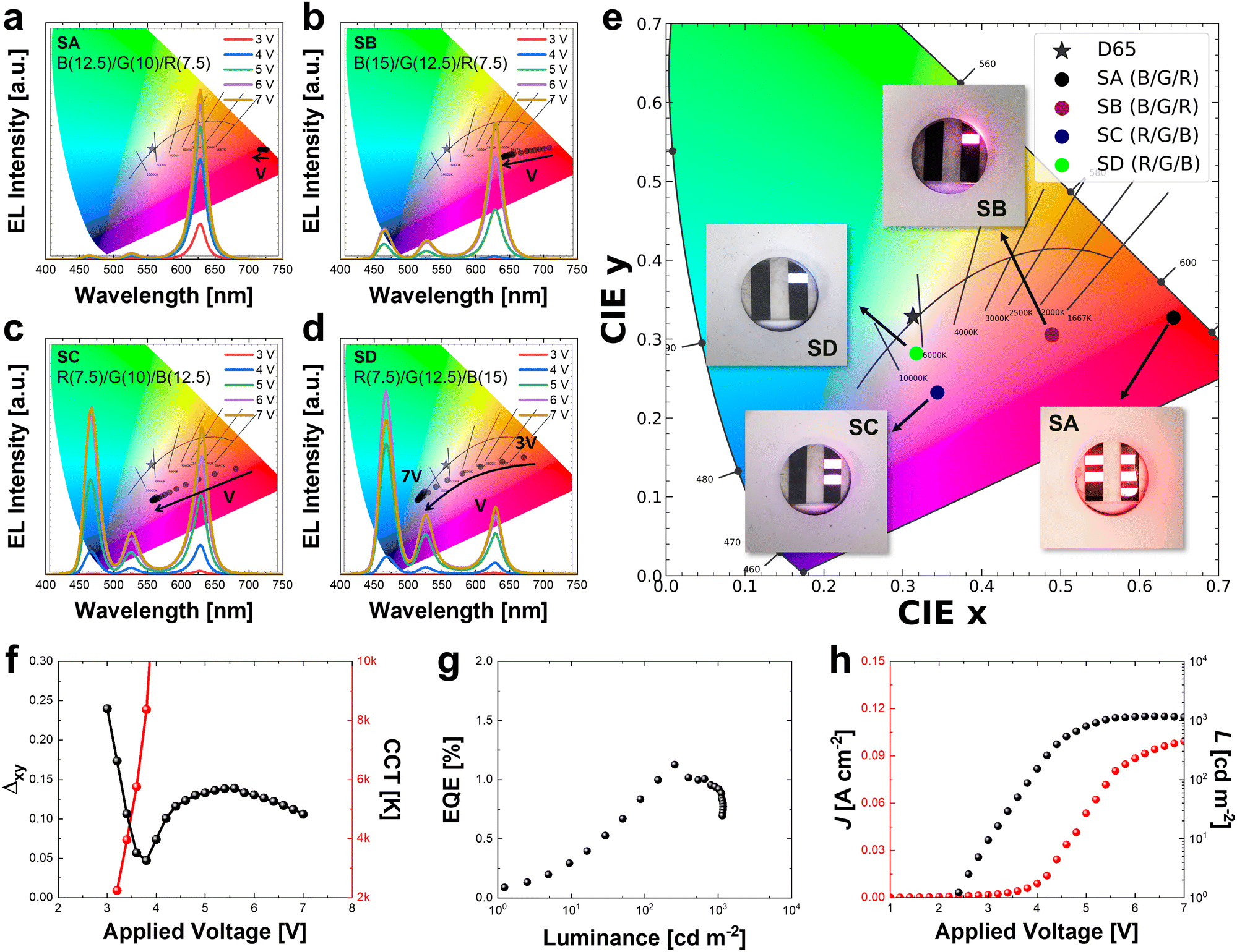 | ||
| Fig. 4 Experimental analysis of the electro-optical properties of the fabricated staked-type QD-LEDs. For the B/G/R stack, the QD layers are stacked onto the HTL surface in the B, G, and R order, while the R, G and B QD layers are sequentially stacked onto the HTL for the R/G/B QD stack. The voltage dependencies of EL spectra and CIE coordinates of the stacked QD-LEDs for (a) the device SA with B(12.5)/G(10)/R(7.5) QD stack, (b) the device SB with B(15)/G(12.5)/R(7.5) QD stack, (c) the device SC with R(7.5)/G(10)/B(12.5) QD stack, and (d) the device SD with R(7.5)/G(12.5)/B(15) QD stack. Numbers in parentheses are the solution concentration of QDs in mg ml−1 unit. (e) CIE color coordinates and the snapshots of the EL-driven devices denoted by SA, SB, SC, and SD. (f) Experimental chromaticity difference and CCT variation for the applied voltage of the fabricated device SD. (g) EQE–luminance curve and (h) experimental current–voltage–luminance curves of the fabricated device SD. | ||
Fig. 4e shows the color coordinates and EL snapshots of the fabricated stacked-type QD-LED devices having different stack sequences and QD concentrations. The B/G/R stacked devices SA and SB show a reddish color with the CCTs of 1563 K and 1611 K, respectively, while the R/G/B stacked devices SC and SD show purple and white colors with CCTs of 6554 K and 6669 K, respectively. From the experimental results, it is confirmed that the color can be predetermined by the stack sequence and QD concentration and that the color variation of the stacked-type QD-LED is mainly determined by the stack sequence of the R, G, and B QD layers.
The chromaticity difference and the CCT of the fabricated stacked device SD of R(7.5)/G(12.5)/B(15) showing the widest color variation and the smallest chromaticity difference are plotted in Fig. 4f for the applied voltage. In Fig. 4f, a minimum chromaticity difference of 0.047 at CIExy of (0.317, 0.281) for white color is observed at the 3.8 V, and the CCT increases abruptly from 2244 K as the voltage increases from 3.2 V. Fig. 4g shows the EQE curve of the fabricated device SD for the luminance. Here, the EQE increases to the maximum of 1.13% but decreases after the maximum as the luminance increases, showing the EQE droop by the Auger recombination caused by the charge imbalance in the QD layers at a high voltage range. Here, the luminance at the maximum EQE was measured and found to be 256 cd m−2. Fig. 4h shows the current density and luminance of the fabricated device SD for the applied voltage. From Fig. 4h, the luminance of the R/G/B stacked white QD-LED was found to be 1171 cd m−2 at an applied voltage of 7.0 V. The voltage at maximum EQE was found to be 4.2 V with a current density of 0.014 A cm−2. The luminance at 3.8 V for the white operation was found to be 87 cd m−2, and its corresponding EQE and CE were measured and were found to be 0.84% and 1.4 cd A−1, respectively (Fig. S6, ESI†).
From the experiments in Fig. 4, it is confirmed that the R/G/B stacked QD-LED exhibits wide color changes with respect to the applied voltage compared to the B/G/R stacked device. Even though the wide color variation is achieved by the R/G/B stacked QD-LED device, the lowest brightness due to insufficient charge transport and optical efficiency caused by the configuration of the multiple QD layers was observed. Moreover, the white chromaticity of the stacked-type QD-LED is a little bit far from the CIE D65 illuminant compared to the patterned-type QD-LED. These are thought to be the reasons that the charge transport and optical efficiency are highly affected by the energy configuration, thickness, and interfacial properties of the multiple QD layers in the stacked-type QD-LED. Together with the device structure, in order to enhance the brightness of the stacked-type white QD-LED device, it is required to enhance the interfacial properties by preventing damage to the underlying QD layer during the multi-step deposition. One of the fabrication methods to avoid interfacial damage is to introduce the buffer layer in between two QD layers with ZnO nanoparticles or to optimize the solvent in the QD solution.37
The stacked-type has more variation such as the thickness of R, G, and B QDs, its interface effect between the stacks, bandgap alignment between each stack of R, G, and B QDs, and location of anode and cathode layers for the hole and electron supply. The stacked type has different thicknesses due to R, G, and B QD stack processing compared to the patterned-type pixel, which could affect electron and hole charge transport. We believe that the hole and electron mobilities are being affected by different transport with respect to the anode and cathode and the interfacial difference between the R, G, and B QD layers. The location of the anode and cathode also plays a critical role in electron and hole supply along the bandgap difference of R/G/B or B/G/R stack. Due to the close vicinity of QD nanoparticles, non-radiative Förster resonant energy transfer (FRET) can take place among the QDs, especially at the interfaces between two different QD layers.38,39 In conclusion, the stacked type has a tendency of lower charge transport possibility and a much lower probability of electron–hole recombination due to the thickness, bandgap alignment, and interfacial layer between the stacks or locations of the anode and cathode. Despite the electro-optical performance, it is worth mentioning from Fig. 4 that the architecture, especially for the stack sequence, highly affects the electro-optical properties of the stacked-type QD-LEDs. Therefore, to explain the experimental architecture dependency on the color properties of the stacked-type QD-LEDs, theoretical analysis by the charge transport simulation is conducted in the following section.
In order to theoretically account for the architectural dependency on the color controllability of the stacked-type QD-LEDs, we performed computational simulations of the stacked-type QD-LED devices with the charge transport model based on the electric-field-dependent carrier hopping process (ESI†). Fig. 5 shows the simulation results of the charge transport model for the R/G/B stacked device (Fig. 5a–c and g) and the B/G/R stacked device (Fig. 5d–f and h).
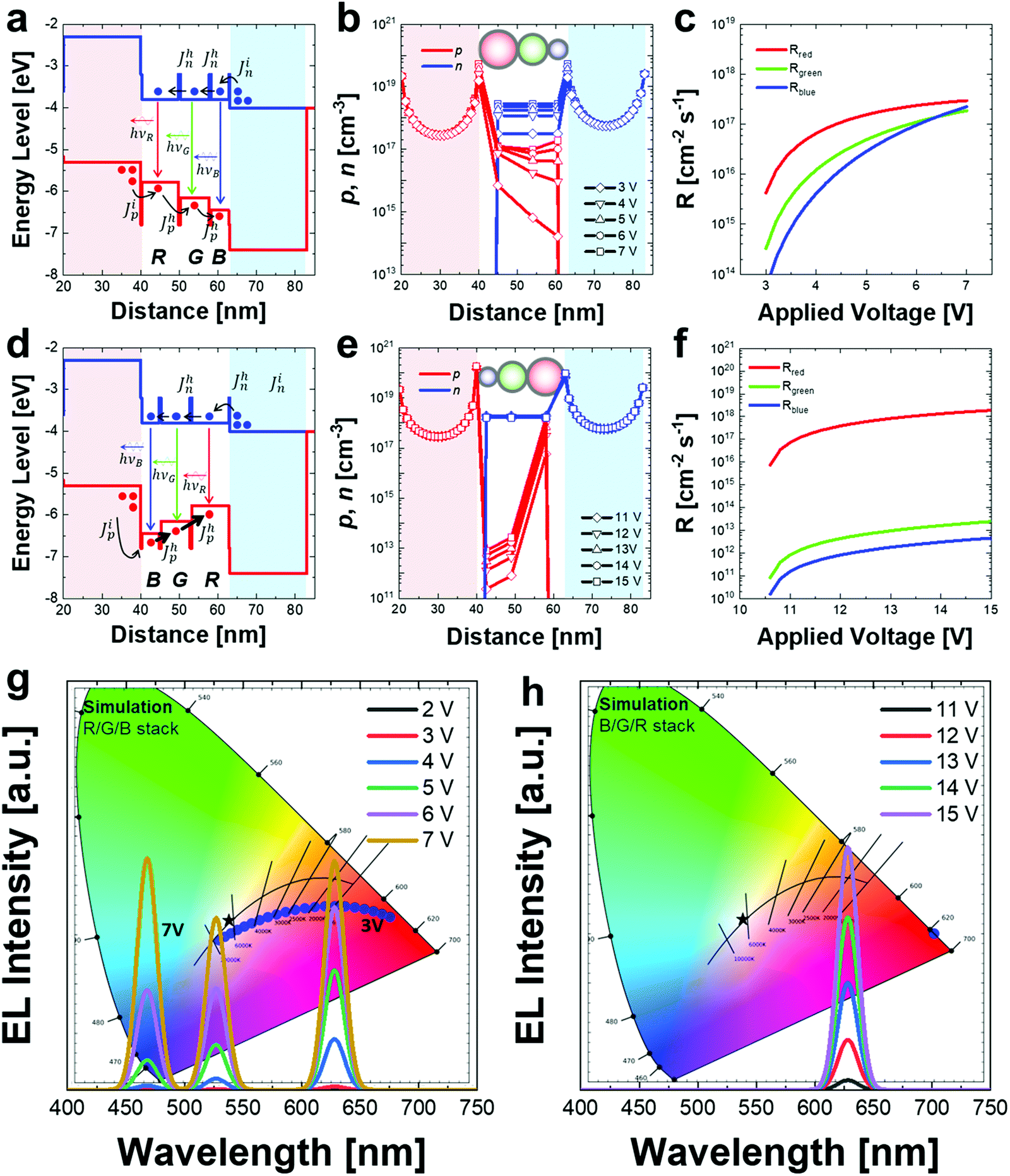 | ||
| Fig. 5 Simulation of the electro-optical properties of R/G/B and B/G/R stacked QD-LEDs. (a) Flat-band energy-level diagram across the R/G/B stacked QD-LED device for the charge transport simulation. (b) Simulated hole and electron densities across the R/G/B stacked device at different voltages. (c) Simulated radiative recombination rate of the R, G, and B QD layers of the R/G/B stacked device for the applied voltage. (d) Flat-band energy-level diagram across the B/G/R stacked QD-LED device for the charge transport simulation. (e) Simulated hole and electron densities across the B/G/R stacked device at different voltages. (f) Simulated radiative recombination rate of the R, G, and B QD layers of the B/G/R stacked device for the applied voltage. Simulated color loci and EL spectra of (g) the R/G/B and (h) the B/G/R stacked devices for the applied voltage. | ||
The flat-band energy-level diagram around the EML of the R/G/B stacked device is plotted in Fig. 5a. For simplicity, the lowest unoccupied molecular orbitals (LUMOs) of the R, G, and B QDs are assumed to be the same as −3.8 eV. The optical bandgaps of the R, G, and B QDs are calculated to be 1.97 eV, 2.35 eV, and 2.65 eV for the experimental EL peak wavelengths of λR = 628 nm, λG = 527 nm, and λB = 468 nm, respectively. Fig. 5b shows the simulated hole and electron density distribution around the EML of the R/G/B stacked QD-LED device. In the conduction band, all QDs have the same electron density due to the same conduction band energy-level. However, in the valence band, even though most of the holes are accumulated at the R QD layer at a low voltage, they are gradually transported to the G and B QD layers as the voltage increases. This is due to the fact that the energy steps to be overcome by the external voltage are built up in the valence band owing to the energy-level configuration of the R/G/B stack device in Fig. 5a. Owing to the dynamic behaviors of the hole and electron with respect to the voltage, the largest rate of the radiative recombination process at the R QD layer is observed at a low voltage. But as the voltage increases, the radiative recombination rates at the G and B QD layers rapidly increase to show the radiative recombination rates at G and B QD layers comparable to the R QD at a high voltage range as shown in Fig. 5c.
The flat-band energy-level diagram of the B/G/R stacked QD-LED device is plotted in Fig. 5d. The hole and electron density distribution around the EML of the B/G/R stacked device is also potted in Fig. 5e. Due to the energy configuration of the B/G/R stacked device in the valence band, most of the holes injected into the EML are directly transported to the R QD layer across the B and G layers by the Boltzmann tunnelling process as shown in Fig. 5e (ESI†).40 As a result, the R QD layer exhibits the highest radiative recombination rate regardless of the voltage changes as shown in Fig. 5f. In Fig. 5e and f, the theoretical threshold voltage of the B/G/R stack is higher than that of the R/G/B stack. Since the valence band offset (the energy difference from the HTL to the adjacent QD layer in the valence band) of the B/G/R stack is relatively higher than that of the R/G/B stack, a higher external voltage is required for the hole to be injected to the QD layer in the B/G/R stack.
Fig. 5g and h show the simulated color loci of the R/G/B and B/G/R stacked QD-LED devices. In Fig. 5g, the color of the R/G/B stacked QD-LED changes from red to blue with respect to the voltage owing to the charge transport behavior in the R/G/B QD stack structure described in Fig. 5a–c. The movement of the simulated color locus with respect to the voltage is very similar to the experimental color loci of the R/G/B stacked device plotted in Fig. 4c and d. Further simulation of the color variation for different energy-level configurations was also performed for the material design of stacked-type white QD-LEDs, and the result is plotted in Fig. S8 (ESI†). Meanwhile, in Fig. 5h, the simulated color of the B/G/R stacked QD-LED hardly changes its color from red even the voltage increases due to the charge transport behavior in the B/G/R stack structure described in Fig. 5d–f.
From Fig. 5, the experimental color behaviors depending on the stack sequence are clearly explained by modelling the R/G/B and B/G/R stacked devices with the electric-field-dependent carrier hopping process and simulating their charge transport together with color properties. From the theoretical simulation, it is confirmed that the major factor determining the color properties of the stacked QD-LED device is the energy-level configuration of the stacked QD layers in the EML. In the experiments and simulation, the R/G/B stacked QD-LED device has a unique energy-level configuration enabling the wide color controllability for the driving voltage. Therefore, it is thought that the R/G/B stacked QD-LED can be applied for lighting such as functionalized mood signages with delicate lighting requiring wide color controllability from red to blue for the driving voltage.
2.4 Electro-optical properties of the mixed-type QD-LED based white lighting device
The use of mixed-type QD-LEDs is the simplest approach to achieving a white lighting system with QD-LEDs. It is fabricated by a solution process via single-step spin-coating by the mixture of the R, G and B QDs in the solution. The EML is a closely packed QD nanoparticle in which R, G, and B QDs are mixed and randomly located in a three-dimensional space. Since the one-dimensional charge transport model is used in this study, the simulation model could not support the three-dimensional configuration of QDs randomly mixed in the EML. Instead, to demonstrate a color variation of QD-LEDs by controlling the volume mixing ratio of RGB QD solution, several kinds of QD solutions have been blended and their corresponding devices have been fabricated. Fig. 6 shows the electro-optical properties of the fabricated mixed-type QD-LEDs for different volume mixing ratios of RGB QD solutions. Fig. 6a–d show the EL intensity spectra of QD-LEDs with R:G:B QD volume mixing ratios for 1:1.5:9 (device MA), 1:2:9 (device MB), 1:4:12 (device MC) and 1:2:18 (device MD), respectively. The EL peak wavelengths λR, λG, and λB of the R, G, and B QDs used in this experiment were measured and found to be 628 nm, 527 nm and 452 nm, respectively. The PL spectrum of the R, G, and B QDs are plotted in Fig. S7 (ESI†). The color changes of each device with respect to the applied voltages are also plotted in each figure. In Fig. 6a, the color of the device MA of a volume mixing ratio of 1:1.5:9 is located around the light purple color with a narrow color variation for the applied voltage. In order to increase the intensity peak of green, more of the green QD was added and the color coordinates close to the white point of the CIE D65 illuminant with a color variation from orange to purple for the applied voltage were obtained by the device MB (Fig. 6b). By adding more amount of green and blue QDs, the blue and green intensity peaks were highly increased, and the bluish color was obtained by the device MC (Fig. 6c). Finally, by adding a large amount of blue QD with less green QD, the intensity peak of blue was dramatically increased, and the resultant darker purple color was obtained by the device MD (Fig. 6d).
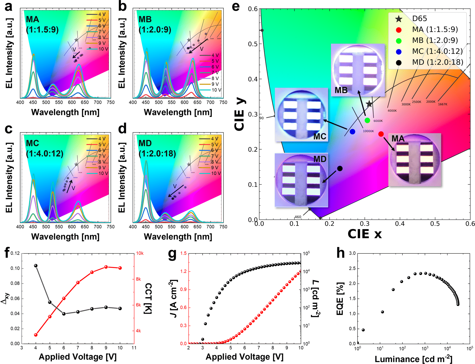 | ||
| Fig. 6 Experimental analysis of the electro-optical properties of mixed-type QD-LEDs. Voltage dependencies of EL spectra and CIE coordinates of the fabricated devices having R:G:B QD volume mixing ratios of (a) 1:1.5:9, (b) 1:2:9, (c) 1:4:12, and (d) 1:2:18. The respective devices are denoted by MA, MB, MC, and MD. (e) CIE color coordinates and the snapshots of the EL-driven devices of the mixed-type QD-LEDs for the devices MA, MB, MC, and MD. (f) Chromaticity difference and CCT variation for the applied voltage of the fabricated device MB. (g) Current density and luminance curves for the voltage and (h) EQE curve of the fabricated device MB for the luminance. | ||
Fig. 6e shows the CIE color coordinates of mixed-type QD-LEDs with different RGB QD volume mixing ratios and their corresponding EL snapshots. The color coordinates of the device MB for the volume mixing ratio of 1:2:9 is closest to the white point, while the color coordinates of the devices MA and MC for 1:1.5:9 and 1:4:12 volume mixing ratios are located far from the white point with light purple and bluish color, respectively. The device MD of 1:2:18 volume mixing ratio is located around darker purple color. From the experimental results, a relatively larger volume mixing ratio of the blue QD is required for the effective amount of blue light to have white chromaticity due to the inter-particle FRET among the QDs and the high energy barrier of B QDs.30,41 From Fig. 6a–e, the mixed-type QD-LED with a volume mixing ratio of 1:2:9 shows the best color properties of chromaticity closest to the D65 illuminant and the widest color variation for the voltage among the various volume mixing ratios.
Fig. 6f shows the experimental chromaticity difference and the CCT variations of the fabricated device MB having a volume mixing ratio of 1:2:9. The color of the device MB is located closest to CIE D65 at an applied voltage of 6 V, and the minimum chromaticity difference and CCT are observed to be 0.040 and 6518 K, respectively. The CCT varies from 3694 K to 8955 K for the voltage change from 4 V to 9 V. Here, the CCT of the device increases gradually for the applied voltage showing a less steep curve compared to the patterned-type and stacked-type QD-LED devices. In Fig. 6g, the current density, luminance, and CE of the device MB at 6 V were measured and found to be 0.246 A cm−2, 9666 cd m−2, and 3.9 cd A−1, respectively, for the white point of the device (Fig. S6, ESI†). The maximum EQE and the EQE at the white point were measured and found to be 2.3% and 2.0%, respectively from Fig. 6h, which show the highest performance among the three types of the QD-LED device architectures.
From Fig. 6, it is found that the color of the mixed-type QD-LED can be predetermined by the volume mixing ratios of the R, G and B QD concentrations in solution. The mixed-type QD-LED shows the highest brightness and EQE at the white operation voltage among the three types of QD-LED device architectures. However, the chromaticity of the mixed-type QD-LED is a little bit far from the CIE D65 illuminant due to the experimental difficulties to control the light contributions of each QDs. This is due to the fact that the QDs in the EML are highly coupled to each other due to the structural complexity of the random mixture. Moreover, a comparably narrow color change for the voltage is observed, which is thought to be an ensemble average effect of the randomness of the QD mixture in the EML. Therefore, it is expected that the mixed-type QD-LED can be used for the application of a white lighting system such as functionalized direct lighting requiring high brightness with simple processibility if the white chromaticity of the mixed-type QD-LED is more precisely controlled by experiments.
The overall electro-optical properties of the three different types of QD-LEDs are summarized in Table 1 and are compared with those from the previous literature in Table S3 (ESI†). As shown in Table S3 (ESI†), the EQEs and the CEs of our white devices are in the middle of those from the previous publications. The device efficiency of the QD-LED is highly affected by the intrinsic properties of QDs. Therefore, by optimizing and developing the QDs customized for each device architecture, it is expected that the efficiencies of the white QD-LED devices can be further improved. The patterned-type QD-LED showed good electro-optical and color performances for smart white lighting devices, exhibiting very wide color controllability and high precision white chromaticity with acceptable brightness. This is due to the ease of designing the device layout owing to its structural uniqueness of clearly separated QD patterns. In contrast, the stacked-type QD-LED exhibited a wide color variation in a small voltage range, requiring highly precise voltage control for the color change. Despite the wide color variation of the stacked-type QD-LED, the lowest brightness due to insufficient charge transport and poor optical efficiency, affected by the energy-level configuration, thickness and interfacial properties of the multiple QD layers, was experimentally observed. The mixed-type QD-LED showed the highest brightness owing to its high quantum efficiency, while a narrow color variation due to the ensemble average effect of the randomness of the QD mixture was observed. For the mixed and stacked types of QD-LEDs, it was difficult to experimentally adjust the precise white chromaticity to the CIE D65 illuminant since the QDs in their EML are highly dependent on each other due to their structural complexity. Nevertheless, more advanced charge transport studies related to the modelling randomized QD layers and interfacial properties among the QD layers are expected in the development of the device architectures of QD-LEDs for next-generation smart white lighting. These three types of patterned, stacked, and mixed QD-LED device architectures can be used for various applications of smart white light systems functionalized by purpose if their electro-optical performances are further advanced through our computational charge transport model and additional experiments.
| Performances | D65 (reference) | Patterned-type | Stacked-type | Mixed-type | |
|---|---|---|---|---|---|
| White point | CIExy | (0.313, 0.329) | (0.314, 0.331) | (0.317, 0.281) | (0.307, 0.282) |
| Δ xy | 0.000 | 0.002 | 0.047 | 0.040 | |
| CCT [K] | 6500 | 6419 | 8368 | 6518 | |
| EQE [%] | — | 0.6 | 0.8 | 2.0 | |
| L [cd m−2] | — | 1830 | 87 | 9666 | |
| V a [V] | — | 5.2 | 3.8 | 6.0 | |
| EL properties | Color | Yellow → blue | Red → blue | Orange → purple | |
| CCT [K] | — | 2998–10000 |
2244–10000 |
3694–8955 | |
| L [cd m−2] | — | 416–3482 |
16–1171 | 365–29850 |
|
| V a [V] | — | 3.6–7.0 | 3.2–7.0 | 4.0–10.0 | |
3. Conclusion
In this study, we have performed a comprehensive analysis and optimization of the electro-optical properties of the three different device architectures of mixed-, stacked-, and patterned-type QD-LEDs for smart white lighting. First, the R, G, and B QD emission pattern layout of the patterned-type QD-LED was optimized through the computational design process with the complete charge transport simulation based on the electric-field-dependent carrier injection model and the numerical grid searching method for color optimization. The optimized patterned-type QD-LED exhibited excellent lighting performances of wide color variation and high precision white chromaticity. Next, the electro-optical properties of the stacked-type QD-LEDs are analyzed by device fabrication and computational charge transport simulation for the R/G/B and B/G/R sequential QD stacks. From the charge transport simulation with the electric-field-dependent carrier hopping model, it was nicely explained that the color properties of the stacked-type QD-LED highly depend on the stack sequence of R, G, and B QD layers determining the energy-level configuration. Finally, the electro-optical properties of the mixed-type QD-LED were experimentally investigated by device fabrication for the different volume mixing ratios in the QD solution mixture. From the experiments, it is confirmed that the white chromaticity of the mixed-type QD-LED is predetermined by the optimal R, G, and B QD volume mixing ratios in the solution mixture. Based on this study, these three types of patterned, stacked, and mixed QD-LED device architectures can be used for various applications of smart white light systems functionalized by purpose if their electro-optical performances are further advanced through our computational charge transport model.Author contributions
D.-W. Shin and S. Lee designed the experiment.; S. Y. Bang, S. D. Han and Y. J. Cho carried out the device fabrication; X.-B. Fan and L. Ni synthesised the materials; H. W. Choi, J.-W. Jo, A. Arbab, J. Yang and Y. Kim supported the experiments and device characterisation; C. Samarakoon and S.-M. Jung developed the simulation model and performed computer simulation; L. G. Occhipinti and G. A. J. Amaratunga performed the analysis of the experimental and simulational data; J. M. Kim conceived the idea and guided this work. All the authors discussed and contributed to the preparation of the manuscript.Conflicts of interest
There are no conflicts to declare.Acknowledgements
This research was supported by the Engineering Physical Sciences Research Council (EPSRC) project EP/P027628/1 ‘Smart Flexible Quantum Dot Lighting’ and the European Commission under H2020 grant agreement No 685758 ‘1D-NEON’. The authors would like to thank Professor Caterina Ducati and May Ching Lai for the measurement and analysis of TEM.References
- A. Kumar, P. Kar, R. Warrier, A. Kajale and S. K. Panda, Energy. Proced., 2017, 143, 173–178 CrossRef.
- B. Bechadergue, L. Chassagne and H. Guan, IEEE Trans. Intell. Veh., 2019, 4, 532–547 Search PubMed.
- S.-H. Yu, O. Shih, H.-M. Tsai, N. Wisitpongphan and R. D. Roberts, IEEE Commun. Mag., 2013, 51, 50–59 Search PubMed.
- A. Pandharipande, M. Zhao and E. Frimout, IEEE Internet Things M., 2019, 2, 22–26 Search PubMed.
- M. Jung, J. Park, P. Premdas, V. Kamp, Y. Zhang, Y. Li and B. Siesegger, 2020 IEEE 6th World Forum on Internet of Things (WF-IoT), IEEE, New Orleans, LA, USA, 2020, pp. 1–6 Search PubMed.
- G. Zissis, Energy Consumption and Environmental and Economic Impact of Lighting: The Current Situation, Springer International Publishing, 2016 Search PubMed.
- E. F. Schubert and J. K. Kim, Science, 2005, 308, 1274–1278 CrossRef CAS PubMed.
- J. Hye Oh, S. Ji Yang and Y. Rag Do, Light: Sci. Appl., 2014, 3, e141 CrossRef.
- S. M. Pauley, Med. Hypotheses, 2004, 63, 588–596 CrossRef PubMed.
- K. V. Danilenko and O. Y. Sergeeva, Neuroendocrinol. Lett., 2015, 36, 84–90 Search PubMed.
- J. Q. Ouyang, S. Davies and D. Dominoni, J. Exp. Biol., 2018, 221, jeb156893 CrossRef PubMed.
- R. H. Friend, R. W. Gymer, A. B. Holmes, J. H. Burroughes, R. N. Marks, C. Taliani, D. D. C. Bradley, D. A. D. Santos, J. L. Brédas, M. Lögdlund and W. R. Salaneck, Nature, 1999, 397, 121–128 CrossRef CAS.
- J. M. Caruge, J. E. Halpert, V. Wood, V. Bulović and M. G. Bawendi, Nat. Photonics, 2008, 2, 247–250 CrossRef CAS.
- S. Nakamura, T. Mukai and M. Senoh, Appl. Phys. Lett., 1994, 64, 1687–1689 CrossRef CAS.
- M. K. Choi, J. Yang, T. Hyeon and D.-H. Kim, npj Flexible Electron., 2018, 2, 10 CrossRef.
- H. Moon, C. Lee, W. Lee, J. Kim and H. Chae, Adv. Mater., 2019, 31, 1804294 CrossRef PubMed.
- O. Chen, J. Zhao, V. P. Chauhan, J. Cui, C. Wong, D. K. Harris, H. Wei, H.-S. Han, D. Fukumura, R. K. Jain and M. G. Bawendi, Nat. Mater., 2013, 12, 445–451 CrossRef CAS PubMed.
- W. K. Bae, Y.-S. Park, J. Lim, D. Lee, L. A. Padilha, H. McDaniel, I. Robel, C. Lee, J. M. Pietryga and V. I. Klimov, Nat. Commun., 2013, 4, 2661 CrossRef PubMed.
- C. R. Kagan, C. B. Murray, M. Nirmal and M. G. Bawendi, Phys. Rev. Lett., 1996, 76, 4 CrossRef PubMed.
- M. Achermann, M. A. Petruska, D. D. Koleske, M. H. Crawford and V. I. Klimov, Nano Lett., 2006, 6, 1396–1400 CrossRef CAS PubMed.
- H.-J. Kim, M.-H. Shin, H.-G. Hong, B.-S. Song, S.-K. Kim, W.-H. Koo, J.-G. Yoon, S.-Y. Yoon and Y.-J. Kim, J. Display Technol., 2016, 12, 526–531 CAS.
- H. Shen, Q. Gao, Y. Zhang, Y. Lin, Q. Lin, Z. Li, L. Chen, Z. Zeng, X. Li, Y. Jia, S. Wang, Z. Du, L. S. Li and Z. Zhang, Nat. Photonics, 2019, 13, 192–197 CrossRef CAS.
- S. Coe, W.-K. Woo, M. Bawendi and V. Bulović, Nature, 2002, 420, 800–803 CrossRef CAS PubMed.
- Y.-H. Won, O. Cho, T. Kim, D.-Y. Chung, T. Kim, H. Chung, H. Jang, J. Lee, D. Kim and E. Jang, Nature, 2019, 575, 634–638 CrossRef CAS PubMed.
- J. M. Pietryga, Y.-S. Park, J. Lim, A. F. Fidler, W. K. Bae, S. Brovelli and V. I. Klimov, Chem. Rev., 2016, 116, 10513–10622 CrossRef CAS PubMed.
- M. K. Choi, J. Yang, K. Kang, D. C. Kim, C. Choi, C. Park, S. J. Kim, S. I. Chae, T.-H. Kim, J. H. Kim, T. Hyeon and D.-H. Kim, Nat. Commun., 2015, 6, 7149 CrossRef CAS PubMed.
- T.-H. Kim, K.-S. Cho, E. K. Lee, S. J. Lee, J. Chae, J. W. Kim, D. H. Kim, J.-Y. Kwon, G. Amaratunga, S. Y. Lee, B. L. Choi, Y. Kuk, J. M. Kim and K. Kim, Nat. Photonics, 2011, 5, 176–182 CrossRef CAS.
- T.-H. Kim, D.-Y. Chung, J. Ku, I. Song, S. Sul, D.-H. Kim, K.-S. Cho, B. L. Choi, J. Min Kim, S. Hwang and K. Kim, Nat. Commun., 2013, 4, 2637 CrossRef PubMed.
- W. K. Bae, J. Kwak, J. Lim, D. Lee, M. K. Nam, K. Char, C. Lee and S. Lee, Nano Lett., 2010, 10, 2368–2373 CrossRef CAS PubMed.
- W. K. Bae, J. Lim, D. Lee, M. Park, H. Lee, J. Kwak, K. Char, C. Lee and S. Lee, Adv. Mater., 2014, 26, 6387–6393 CrossRef CAS PubMed.
- P. O. Anikeeva, J. E. Halpert, M. G. Bawendi and V. Bulović, Nano Lett., 2007, 7, 2196–2200 CrossRef CAS PubMed.
- B. Kumar, S. A. Campbell and P. Paul Ruden, J. Appl. Phys., 2013, 114, 044507 CrossRef.
- S.-M. Jung, T. H. Lee, S. Y. Bang, S. D. Han, D.-W. Shin, S. Lee, H. W. Choi, Y.-H. Suh, X.-B. Fan, J.-W. Jo, S. Zhan, J. Yang, C. Samarakoon, Y. Kim, L. G. Occhipinti, G. Amaratunga and J. M. Kim, npj Comput. Mater., 2021, 7, 122 CrossRef CAS.
- CIE and CUPC, Commission internationale de l’eclairage proceedings, Cambridge University, 1932 Search PubMed.
- T. M. Mansencal, M. Parsons, M. Canavan, L. Cooper, S. Shaw, N. Wheatley, K. Crowson and K. L. Ofek, Colour Science for Python 0.3.11, 2018 Search PubMed.
- S. A. Empedocles and M. G. Bawendi, Science, 1997, 278, 2114–2117 CrossRef CAS PubMed.
- K.-H. Lee, C.-Y. Han, E.-P. Jang, J.-H. Jo, S. Hong, J. Y. Hwang, E. Choi, J.-H. Hwang and H. Yang, Nanoscale, 2018, 10, 6300–6305 RSC.
- K. Chou and A. Dennis, Sensors, 2015, 15, 13288–13325 CrossRef PubMed.
- H. Zhang, Q. Su, Y. Sun and S. Chen, Adv. Opt. Mater., 2018, 6, 1800354 CrossRef.
- C. Fazio, O. R. Battaglia and I. Guastella, Eur. J. Phys., 2012, 33, 359–371 CrossRef.
- K.-H. Lee, C.-Y. Han, H.-D. Kang, H. Ko, C. Lee, J. Lee, N. Myoung, S.-Y. Yim and H. Yang, ACS Nano, 2015, 9, 10941–10949 CrossRef CAS PubMed.
Footnotes |
| † Electronic supplementary information (ESI) available. See DOI: https://doi.org/10.1039/d2tc01060g |
| ‡ D.-W S. and S. L. contributed equally to this work. |
| This journal is © The Royal Society of Chemistry 2022 |