
 Open Access Article
 This Open Access Article is licensed under a Creative Commons Attribution-Non Commercial 3.0 Unported Licence
Charge transfer complexes of a benzothienobenzothiophene derivative and their implementation as active layer in solution-processed thin film organic field-effect transistors†
Lamiaa
Fijahi
 a,
Tommaso
Salzillo‡
*a,
Adrián
Tamayo
a,
Marco
Bardini
b,
Christian
Ruzié
c,
Claudio
Quarti
b,
David
Beljonne
*b,
Simone
d’Agostino
*d,
Yves H.
Geerts
c and
Marta
Mas-Torrent
*a
a,
Tommaso
Salzillo‡
*a,
Adrián
Tamayo
a,
Marco
Bardini
b,
Christian
Ruzié
c,
Claudio
Quarti
b,
David
Beljonne
*b,
Simone
d’Agostino
*d,
Yves H.
Geerts
c and
Marta
Mas-Torrent
*a
aInstitut de Ciència de Materials de Barcelona (ICMAB-CSIC), Campus de la UAB, 08193 Bellaterra, Barcelona, Spain. E-mail: mmas@icmab.es
bLaboratory for Chemistry of Novel Materials, University of Mons, 7000 Mons, Belgium. E-mail: David.Beljonne@umons.ac.be
cInternational Solvay Institutes of Physics and Chemistry and Laboratoire de Chimie des Polymères, Faculté des Sciences, Université Libre de Bruxelles (ULB), CP 206/01, Boulevard du Triomphe, 1050, Brussels, Belgium
dChemistry Department “Giacomo Ciamician”, University of Bologna, Via F. Selmi 2, 40126 Bologna, Italy. E-mail: simone.dagostino2@unibo.it
First published on 13th April 2022
Abstract
Herein, we report on the synthesis and structural characterization of novel charge transfer (CT) complexes of the benzothienobenzothiophene derivative C8O-BTBT-OC8 with the series of FxTCNQ derivatives (x = 2, 4). The degree of charge transfer and HOMO–LUMO gap energies were evaluated by spectroscopic means and by DFT calculations. Thin films of the (C8O-BTBT-OC8)(F4TCNQ) complex were prepared by a simple solution shearing technique and by blending the active materials with polystyrene. X-Ray diffraction and IR/Raman spectroscopy techniques were instrumental for the structural identification of the films, which belonged to the same phase as the resolved single crystal. The films were implemented as an active layer in organic field-effect transistor (OFET) devices, which exhibited an n-type behavior in ambient conditions in agreement with the theoretical calculations.
Introduction
Organic charge-transfer (CT) complexes are two component systems formed by an electron Donor (D) and an electron Acceptor (A) unit with a specific stoichiometry. These binary systems are characterised by a charge transfer state with a certain ionicity (ρ) that can range from neutral (ρ = 0) to the fully ionised form (ρ = 1). The degree of charge transfer depends on the chemical structure of their constituents, but also on the overlap between their frontier molecular orbitals. Typically, D/A CT single crystals organise in either segregated (i.e., –D–D–D– and A–A–A–) or mixed (i.e., –D–A–D–A–) π-stacks. Both the packing and charge transfer degree importantly determine the resulting electrical properties, which can vary from insulator, semiconductor, and metallic to superconductor.1,2 For many decades CT complexes were intensively investigated in order to establish guidelines to design materials exhibiting high room-temperature mobility or superconductivity.3 However, in the more recent years, the focus has also been placed on the development of more technologically relevant applications deploying such CT complexes,4–6 including thermoelectrics,7 photoconductors,8,9 strain sensors,10 light detectors,11 ferroelectrics12 or organic field-effect transistors (OFETs), where CT complexes can act as organic metals13,14 or organic semiconductors.15,16The separate D or A units in a CT complex typically can act as unipolar (p and n, respectively) organic semiconductors when implemented in an OFET.17,18 However, when they co-crystallise together, they can exhibit completely different properties. Hence, significant efforts are being devoted on exploring the electrical performance of a variety of CT systems as active layers in OFETs. Nonetheless, these studies have been mainly restricted to prototypical single crystals or co-evaporated thin films, which are not desirable for practical applications.19–21 Indeed, the preparation of thin films of CT complexes over large areas employing solution-based techniques is highly challenging since the solubility of the separate components in organic solvents is distinct to the one from the CT complex. Recently, we reported the fabrication of thin films of the CT complex dibenzotetrathiafulvalene-7,7,8,8-tetracyanoquinodimethane (DBTTF)(TCNQ) employing a solution shearing deposition technique.17,18 This was achieved by blending the CT complex with an insulating binding polymer to promote film processability and crystallinity.
Here, we report the preparation and characterisation of two novel CT crystals based on 2,7-bis(octyloxy)[1]benzothieno[3,2-b]-benzothiophene (C8O-BTBT-OC8) and fluorinated 7,7,8,8-tetracyanoquinodimethane (i.e., F2TCNQ and F4TCNQ) (Scheme 1). In both cases, the donor and acceptor molecules co-crystallise in a 1![[thin space (1/6-em)]](https://www.rsc.org/images/entities/char_2009.gif) :1 stoichiometry forming stacks of alternating C8O-BTBT-OC8 and F2TCNQ or F4TCNQ. A low charge transfer degree is found for the CT complex based on F2TCNQ, whereas this value is increased with the more electron acceptor F4TCNQ derivative. Further, thin films of (C8O-BTBT-OC8)(F4TCNQ), corresponding to the same crystal phase as the single crystal one, were successfully prepared employing a high throughput solution-based deposition technique in ambient conditions. The films were characterised as active layer in OFETs giving an n-type behaviour.
:1 stoichiometry forming stacks of alternating C8O-BTBT-OC8 and F2TCNQ or F4TCNQ. A low charge transfer degree is found for the CT complex based on F2TCNQ, whereas this value is increased with the more electron acceptor F4TCNQ derivative. Further, thin films of (C8O-BTBT-OC8)(F4TCNQ), corresponding to the same crystal phase as the single crystal one, were successfully prepared employing a high throughput solution-based deposition technique in ambient conditions. The films were characterised as active layer in OFETs giving an n-type behaviour.
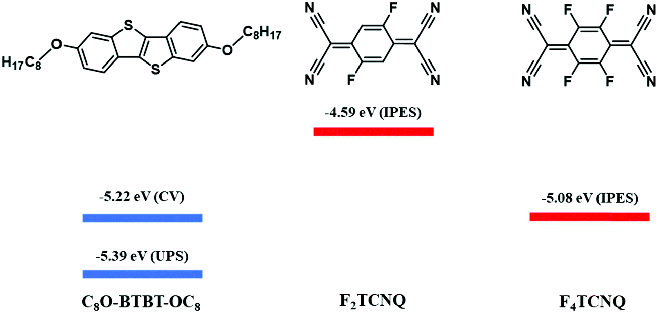 | ||
| Scheme 1 Molecular structures of the donor (C8O-BTBT-OC8) and acceptor (F2TCNQ and F4TCNQ) compounds, and HOMO (blue) and LUMO (red) energy levels for C8O-BTBT-OC8, F2TCNQ, and F4TCNQ.22,23 The LUMO levels of the acceptor molecules were estimated by Inverse Photoemission Spectroscopy (IPES). The HOMO levels of C8O-BTBT-OC8 estimated by Cyclic Voltammetry (CV) and Ultra-Violet Photoelectron Spectroscopy (UPS) are shown. | ||
Results and discussions
The BTBT derivative C8O-BTBT-OC8 (Scheme 1) has previously been reported as a highly promising p-type organic semiconductor.22,24 However, CT complexes with this derivative have never been reported before. CT complexes based on C8O-BTBT-OC8 with TCNQ, F2TCNQ and F4TCNQ were attempted to grow, although with the non-fluorinated acceptor no complex was formed. The latter cannot be explained by the mismatch of the highest occupied molecular orbital (HOMO) of the donor with the lowest unoccupied molecular orbital (LUMO) of the acceptor,25 since CT complexes with TCNQ have been reported for other BTBT derivatives, with even deeper HOMO level.6,20,21,26–28Both CT complexes, (C8O-BTBT-OC8)(F2TCNQ) and (C8O-BTBT-OC8)(F4TCNQ), crystallize as isomorphous in the triclinic P![[1 with combining macron]](https://www.rsc.org/images/entities/char_0031_0304.gif) space group (see Table S1 for details and Fig. S1, ESI†), and feature extended stacks, running along the a-axis, in which molecules of the donor C8O-BTBT-OC8 alternate with the corresponding acceptor TCNQ-derivative in an ⋯A⋯D⋯A⋯D⋯ fashion (Fig. 1). Despite the different nature of the TCNQ acceptor, the interplanar distances (plane to centroid) between C8O-BTBT-OC8 and F2TCNQ or F4TCNQ are only slightly different, accounting for 3.3 Å and 3.2 Å, respectively, which are slightly shorter compared with CT complexes made of analog BTBT donor derivatives.26,27 In both cases, the indexing of the crystal faces revealed that the long crystal axis corresponds to the crystallographic [1 0 0] direction, and hence, the π⋯π stacking direction (Fig. S2 and S3, ESI†). Additionally, it is worth noting how both (C8O-BTBT-OC8)(F2TCNQ) and (C8O-BTBT-OC8)(F4TCNQ) display a remarked structural resemblance with other CT complexes made up of alkylated benzothienobenzothiophene and TCNQ derivatives, which were previously reported as promising candidates for the development of OSCs.6
space group (see Table S1 for details and Fig. S1, ESI†), and feature extended stacks, running along the a-axis, in which molecules of the donor C8O-BTBT-OC8 alternate with the corresponding acceptor TCNQ-derivative in an ⋯A⋯D⋯A⋯D⋯ fashion (Fig. 1). Despite the different nature of the TCNQ acceptor, the interplanar distances (plane to centroid) between C8O-BTBT-OC8 and F2TCNQ or F4TCNQ are only slightly different, accounting for 3.3 Å and 3.2 Å, respectively, which are slightly shorter compared with CT complexes made of analog BTBT donor derivatives.26,27 In both cases, the indexing of the crystal faces revealed that the long crystal axis corresponds to the crystallographic [1 0 0] direction, and hence, the π⋯π stacking direction (Fig. S2 and S3, ESI†). Additionally, it is worth noting how both (C8O-BTBT-OC8)(F2TCNQ) and (C8O-BTBT-OC8)(F4TCNQ) display a remarked structural resemblance with other CT complexes made up of alkylated benzothienobenzothiophene and TCNQ derivatives, which were previously reported as promising candidates for the development of OSCs.6
 | ||
| Fig. 1 Structural features of crystalline (C8O-BTBT-OC8)(F4TCNQ): (a) molecular structure of the CT complex as observed in its crystal, and (b) side and top views of the columnar stacking running along the a-axis. C-atoms of C8O-BTBT-OC8 and F4TCNQ molecules in grey and orange, respectively. | ||
Raman and Infrared (IR) spectroscopy are non-destructive techniques very useful for the characterisation of CT complexes since it is well known that charge transfer interactions influence some vibrational modes of both donor and acceptor. Here, Raman spectra of the single crystal CT complexes were compared with the ones of the parent compounds (Fig. 2). For the TCNQ derivatives two Raman active modes have been identified to be sensitive29,30 to the degree of charge transferred from the donor to the acceptor: the stretching of the C![[double bond, length as m-dash]](https://www.rsc.org/images/entities/char_e001.gif) C double bonds of the central TCNQ core and the stretching of the periferic CN groups. For the (C8O-BTBT-OC8)(F2TCNQ) complex, the CC stretching shifts from 1456.7 to 1449.2 cm−1 and the CN from 2230.1 to 2220.6 cm−1, whereas in the case of (C8O-BTBT-OC8)(F4TCNQ) the CC stretching shifts from 1454.8 to 1442.9 cm−1 and the CN from 2224.5 to 2218.7 cm−1. This phenomena clearly indicates that a certain charge transfer degree between the donor and the acceptor unit in both CT complexes is occurring.
C double bonds of the central TCNQ core and the stretching of the periferic CN groups. For the (C8O-BTBT-OC8)(F2TCNQ) complex, the CC stretching shifts from 1456.7 to 1449.2 cm−1 and the CN from 2230.1 to 2220.6 cm−1, whereas in the case of (C8O-BTBT-OC8)(F4TCNQ) the CC stretching shifts from 1454.8 to 1442.9 cm−1 and the CN from 2224.5 to 2218.7 cm−1. This phenomena clearly indicates that a certain charge transfer degree between the donor and the acceptor unit in both CT complexes is occurring.
 | ||
| Fig. 2 Raman spectra of (a) (C8O-BTBT-OC8)(F2TCNQ) and (b) (C8O-BTBT-OC8)(F4TCNQ). The CC and CN charge sensitive modes are marked with an asterisk. | ||
As previously mentioned, the ionicity (ρ) is a key parameter in CT complexes. There are several experimental methods which have been reported so far to determine ρ. The most common one is using vibrational spectroscopy by checking the shift of the so called “charge sensitive modes” as mentioned above for the Raman spectra. However, it has been reported that for mixed stack CT systems Raman spectroscopy is not the best option for the determination of ρ due to its overestimation because these modes are affected by the electron–phonon (or electron-molecular vibration) coupling.30,31 Instead, IR modes are more reliable. Again, for CT complexes based on FxTCNQ, the stretching of the CN periferic groups and C–C bonds have been identified to be charge sensitive.29 Considering that often the CN group is influenced by the intermolecular interaction network, the more reliable charge sensitive modes to estimate ρ are the three ones attributed to the C–C bonds (Fig. 3a). These modes appear at the following frequencies: v1: 1577 cm−1 and 1598 cm−1; v2: 1551 cm−1 and 1550 cm−1; v3: 1396 cm−1 and 1395 cm−1, for F2TCNQ and F4TCNQ, respectively.18,29,30 The IR spectra of the prepared C8O-BTBT-OC8 CT complexes are shown in Fig. 3b and c together with the ones of the separate components. From the shift of the CN stretching (from 2230.2 to 2221.9 cm−1 for (C8O-BTBT-OC8)(F2TCNQ) and from 2227.0 to 2221.8 cm−1 for (C8O-BTBT-OC8)(F4TCNQ)) the CT interaction is confirmed in agreement with the Raman results. Furthermore, two of the three C–C charge sensitive modes are identified and marked on the IR spectrum (v1: 1385.8 and 1386.3 cm−1 and v3: 1572.2 and 1583.4 cm−1 for the F2TCNQ and F4TCNQ CT complex, respectively). The vibration v2 is probably too weak to be detected. Assuming a linear correlation between ρ and the frequency shifts, and knowing the frequencies of the modes v1 and v3 of the neutral (i.e., F2TCNQ and F4TCNQ) and completely ionic (i.e., K+F2TCNQ and K+F4TCNQ) species,29 the ρ of the CT complexes was calculated. Accordingly, the estimated degree of ionicity was found to be 0.16 and 0.29 for (C8O-BTBT-OC8)(F2TCNQ) and (C8O-BTBT-OC8)(F4TCNQ), respectively. It is worth noting that v3 is very close to a vibration of the donor C8O-BTBT-OC8, which could generate certain underestimation of the degree of ionicity. These results show that a higher degree of CT is found with the more electron acceptor F4TCNQ (Scheme 1). Further, it is noticed that the ionicity in these derivatives is higher than the previously reported values found for BTBT and di-alkyl BTBT analogous CT complexes.25,26
 | ||
| Fig. 3 (a) C–C charge sensitive modes for F4TCNQ. (b) IR spectra of C8O-BTBT-OC8, F2TCNQ and the corresponding CT complex. (c) IR spectra of C8O-BTBT-OC8, F4TCNQ and the corresponding CT complex. The C–C charge sensitive modes are marked with an asterisk. | ||
The optical HOMO–LUMO gap energies of the CT complexes were subsequently estimated by UV-Vis-NIR spectroscopy (Fig. S4, ESI†). This is realized according to the following equation:32

Solid-state Density Functional Theory (DFT) electronic structure calculations were performed for the (C8O-BTBT-OC8)(FxTCNQ) co-crystals using the hybrid B3LYP functional on the basis of the experimental single crystal X-ray structures. Mülliken population analysis yields an ionicity parameter ρ of 0.098 in (C8O-BTBT-OC8)(F2TCNQ) and of 0.128 in (C8O-BTBT-OC8)(F4TCNQ). We note that these values are larger than those obtained using a similar modeling protocol by Ashokan et al.25 (ρ ∼ 0.07 in (C8-BTBT-C8)(F2TCNQ) and (C8-BTBT-C8)(F4TCNQ)) in the case of co-crystals involving the same acceptors but alkylated instead of alkoxylated BTBT derivatives as donors. Such a difference is associated with the stronger donor character of the C8O-BTBT-OC8 molecules induced by the electron pushing alkoxy moieties. The calculated ionicities are in good qualitative agreement with experiment (namely reproduce the trend observed with increasing strength of the acceptor), yet are slightly lower than the values of ∼0.16 in (C8O-BTBT-OC8)(F2TCNQ) and ∼0.29 in (C8O-BTBT-OC8)(F4TCNQ) inferred from the measured vibrational spectra. Such a discrepancy is either due to the metric adopted to probe the degree of charge transfer or to the level of theory used (as pointed out in ref. 25 a proper description of the degree of ionicity in these crystals would require the use of optimally-tuned range separated functionals, currently not implemented), or a combination of both.
The DFT calculated band structures of the (C8O-BTBT-OC8)(F4TCNQ) and (C8O-BTBT-OC8)(F2TCNQ) co-crystals are reported in Fig. 4 and the extracted hole and electron effective masses collected in Table 1. Similar to the case of alkylated BTBT in ref. 25 we expect electrical transport in these co-crystals to be: (i) strongly anisotropic and predominantly one-dimensional, with much lower effective masses along the D:A stacking direction (see Table S2, ESI†); and (ii) dominated by electrons, with effective masses significantly smaller than the corresponding values for holes. Additionally, the DFT calculated electronic bandgaps of 1.19 (0.89) eV in the F2TCNQ (F4TCNQ) doped co-crystal match reasonably well the measured optical gap of ∼0.96 (∼0.80) eV, though the comparison should be considered with care as electron–hole correlations are not included in the calculations.
 | ||
| Fig. 4 Band structures of (C8O-BTBT-OC8)(F4TCNQ) (bottom) and (C8O-BTBT-OC8)(F2TCNQ) (top). The direct lattice directions corresponding to the reciprocal lattice pathway are indicated on the X axis. | ||
| Co-crystals | Bandwidth (meV) | Effective mass (m*/m0) | ||
|---|---|---|---|---|
| CB | VB | Electrons | Holes | |
| a Ref. 25. b This work. | ||||
| (C8-BTBT-C8)(TCNQ)a | 280 | 82 | 1.0 | 3.1 |
| (C8-BTBT-C8)(F4TCNQ)a | 329 | 128 | 0.7 | 1.5 |
| (C12-BTBT-C12)(TCNQ)a | 280 | 88 | 1.2 | 3.9 |
| (C12-BTBT-C12)(F4TCNQ)a | 316 | 110 | 1.1 | 3.6 |
| (C8O-BTBT-OC8)(F2TCNQ)b | 357 | 174 | 1.8 | 3.1 |
| (C8O-BTBT-OC8)(F4TCNQ)b | 408 | 244 | 1.4 | 2.0 |
Once characterised the single crystal CT complexes, we aimed at investigating their potential as organic semicondutors in OFETs. However, due to the difficulty of handling single crystals and their limited practical applicability, we focused on the preparation of thin films by a high throughput solution-based technique. The bar-assisted meniscus shearing (BAMS) technique was employed, which was previously used successfully to deposit a large family of organic semiconductors and a CT complex (Fig. 5a).18,33–38 This technique consists in placing a solution of the organic material between a bar and a heated substrate forming a confined meniscus and, immediately afterwards, displacing the substrate at a constant speed. It has also been shown that the use of polymer blends facilitates the processing of the films, the crystallisation of the semiconductor and the device stability.39–42
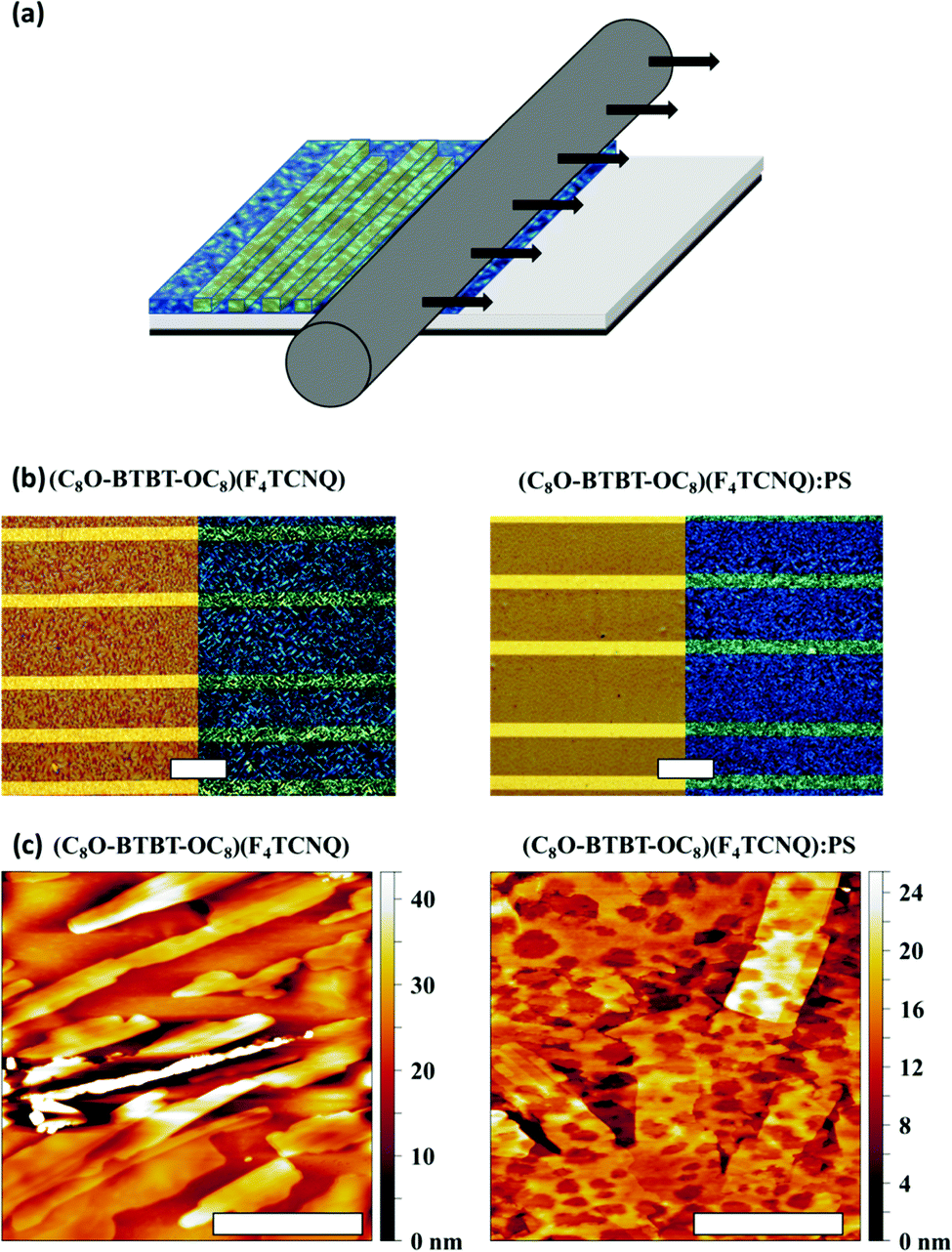 | ||
| Fig. 5 (a) Schematic illustration of the BAMS technique. (b) Non polarized and polarized optical microscopy images with crossed polarizer/analyzer setup of (C8O-BTBT-OC8)(F4TCNQ) and (C8O-BTBT-OC8)(F4TCNQ):PS films. Scale bar: 100 μm. (c) AFM topography images of (C8O-BTBT-OC8)(F4TCNQ) and (C8O-BTBT-OC8)(F4TCNQ):PS films. Scale bar: 2 μm. | ||
After an optimisation process modifying the solution formulation (solvent and molecular weight and ratio of the polymer binder) and coating conditions (i.e., temperature and speed), thin films of (C8O-BTBT-OC8)(F2TCNQ) and (C8O-BTBT-OC8)(F4TCNQ) were prepared using: (1) a 2 wt% solution of an equimolar ratio of C8O-BTBT-OC8 and FxTCNQ in a mixture of chlorobenzene:benzonitrile (5:1), and (2) blending the solution prepared in (1) with a 2 wt% solution of polystyrene (PS) 280 kg mol−1 in the same mixture of solvents in a ratio 4:1. The solutions were kept at high temperature to avoid precipitation of the materials. The deposition was performed at a speed of 2 mm s−1 and keeping the substrate at 85 °C. Homogenous thin films of (C8O-BTBT-OC8)(F4TCNQ) were successfully prepared. However, the films were not highly reproducibly fabricated with the CT (C8O-BTBT-OC8)(F2TCNQ). Therefore, the following studies were focused only on thin films of (C8O-BTBT-OC8)(F4TCNQ).
To assess the morphology and crystallinity of the semiconducting layer, optical polarised microscopy images of the thin films were taken and are shown in Fig. 5b. Both films (i.e., with and without PS) show a similar polycrystalline morphology with small domains A closer analysis by Atomic Force Microscopy (AFM) reveal that the films are formed by small stripe-shaped crystals without any preferential orientation along the surface (Fig. 5c). The thickness of (C8O-BTBT-OC8)(F4TCNQ) films was found to be (29.7 ± 8.4) nm with a route mean square roughness (Rrms) of 7.9 ± 6.3 nm, whereas (C8O-BTBT-OC8)(F4TCNQ):PS films were 23.8 ± 9.1 nm thick with a Rrms of 5.6 ± 2.1 nm.
In order to verify if the thin film corresponds to same crystal phase as the single crystal one described above, X-ray diffraction (XRD) along with spectroscopic characterization were carried out. Both XRD of the films with and without PS reveal two main peaks attributed to the (001) and (002) reflections that coincide with the single crystal structure (Fig. 6a). Moreover, the XRD data indicates that the crystals are oriented with the ab plane parallel to the substrate, and hence the stacking direction, that should coincide with the most favourable transport path, is parallel to the substrate.
 | ||
| Fig. 6 (a) XRD diffractograms of thin films of (C8O-BTBT-OC8)(F4TCNQ) and (C8O-BTBT-OC8)(F4TCNQ):PS. (b) Raman spectra of a (C8O-BTBT-OC8)(F4TCNQ) thin film and the one corresponding to the single crystal. (c) IRRAS spectra of (C8O-BTBT-OC8)(F4TCNQ):PS, (C8O-BTBT-OC8)(F4TCNQ) and PS thin films. The relevant charge sensitive modes are marked with an asterisk. | ||
Fig. 6b shows the Raman characterisation performed on thin films of (C8O-BTBT-OC8)(F4TCNQ) together with the one recorded for the single crystal for comparison. Interestingly, the shifts of the C–C and CN stretchings appear in the film at 1442.9 cm−1 and 2218.7 cm−1, respectively, which perfectly match the ones previously found for the single crystal. The thin films were also inspected by Infrared Reflection–Absorption Spectroscopy (IRRAS). The frequencies of the C–C modes v1 and v3 are difficult to assign unambiguously (Fig, S5, ESI†). On the other hand, the CN stretching is clearly observed as in the single crystal at 2219 cm−1 (Fig. 6c), confirming the formation of the CT salt in the film.
Both (C8O-BTBT-OC8)(F4TCNQ) and (C8O-BTBT-OC8)(F4TCNQ):PS films were electrically characterized as active layers in OFETs under ambient conditions. Fig. 7 shows representative transfer characteristics (see Fig. S6 for the mobility profile and Fig. S7, ESI† for the output characteristics). All the devices exhibit n-type OFET behaviour, with an average electron mobility of 1.0 ± 0.2 × 10⁻³ cm2 V−1 s−1 and threshold voltage of 1.6 ± 6.4 V for the films with PS binder, while for pristine films the mobility was 1.4 ± 0.3 × 10⁻⁴ cm2 V−1 s−1 and the threshold voltage 11.3 ± 5.2 V (values averaged from three substrate coatings containing at least 12 devices each). Hence, the addition of the PS binder polymer increases the device mobility in one order of magnitude and reduces the threshold voltage. Such device improvement can be attributed to a decrease in the interfacial charge trap density produced by the passivation of the SiO2 dielectric with PS.41,43,44 Further, the device electrical characteristics are consistent with the performed DFT calculations, which indicated that transport in this co-crystal should be dominated by electrons. It should be also noticed that the device mobility achieved with the blended films is of the same order as the values reported for analogous evaporated films based on different BTBT derivatives.16,21 Although CT complexes could in principle show ambipolar transport,18,45–48 complexes based on BTBT and fluorinated TCNQ typically have shown only n-type behavior.20,21,27,49 This has been partly attributed to the energy matching between the Fermi level of the Au electrodes and the frontier molecular orbitals of the CT system.16,20,21 Indeed, the energy levels (C8O-BTBT-OC8)(F4TCNQ) are mainly determined by the HOMO of the donor and the LUMO of the acceptor.16 Since the F4TCNQ LUMO level is close the Au work-function (i.e., the metal used for the source-drain contacts), the injection of electrons is more favourable in this device configuration.
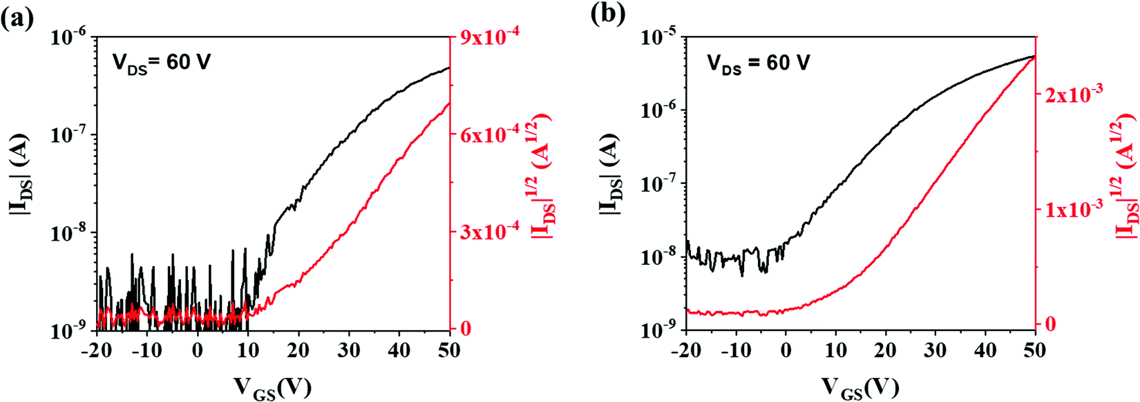 | ||
| Fig. 7 Transfer characteristics of the OFETs based on (a) (C8O-BTBT-OC8)(F4TCNQ) and (b) (C8O-BTBT-OC8)(F4TCNQ):PS. The channel length is 150 μm and the width/length ratio is 100. | ||
Generally, n-channel OFETs suffer from air-instability because the presence of water and oxygen reduces the device performance. This particularly applies to thin film transistors, including F4TCNQ. However, it has been claimed that two-component molecular compounds composed of TCNQ are much more stable due to the intermolecular CT interaction in the solid state.20,27 Importantly to highlight is that the devices were here prepared and measured completely under ambient conditions. Further, around 40% of the prepared devices based on (C8O-BTBT-OC8)(F4TCNQ):PS were still operating properly after 30 days stored in environmental conditions, although this percentage decreased to 20–25% for the non-blended films.
In conclusion, we prepared and characterised two new CT crystals based on the organic semiconductor C8O-BTBT-OC8, namely (C8O-BTBT-OC8)(F2TCNQ) and (C8O-BTBT-OC8)(F4TCNQ). Both systems crystallise in a 1:1 stoichiometry forming alternating stacks of C8O-BTBT-OC8 and F2TCNQ or F4TCNQ. The ionicity was estimated by spectroscopic means to be 0.16 for (C8O-BTBT-OC8)(F2TCNQ) and increased to 0.29 for (C8O-BTBT-OC8)(F4TCNQ). Similar results were found using DFT calculations, which showed the same tendency in which a higher charge transfer is occurring with the more electron acceptor unit F4TCNQ. In addition, homogenous thin films based on the CT (C8O-BTBT-OC8)(F4TCNQ) and (C8O-BTBT-OC8)(F4TCNQ) blended with PS, were successfully prepared employing a solution-based technique compatible with roll-to-roll processes in ambient conditions. By a combination of XRD and spectroscopic techniques it was proved that the films are based on the same phase as the single crystal. Importantly, the films were implemented as active layers in OFETs, showing an n-type behaviour, in agreement with DFT calculations that pointed that transport in this co-crystal is dominated by electrons. This work shows that CT complexes are highly appealing materials for their unique tuneable electrical properties and can, in addition, potentially have applicability in devices by finding suitable routes to process them as thin films deploying low-cost solution-based techniques.
Experimental section
Materials and methods
C8O-BTBT-OC8, synthesized by the procedure previously described.22 Polystyrene (PS) 280 kDa and 2,3,4,5,6-pentafluorothiophenol (PFBT) were purchased from Sigma-Aldrich and used without further purification. All the solvents (from Aldrich) were of spectroscopic grade.Synthesis and crystal growth
CT complexes of C8O-BTBT-OC8/FxTCNQ were prepared by dissolving an equimolar amount of C8O-BTBT-OC8 and F2TCNQ or F4TCNQ in the mixed solvent toluene:acetonitrile 5:1. The resulting solutions were heated at 80 °C for one hour to ensure the complete dissolution of the components; then, they were left to cool down in ambient conditions in the dark overnight slowly. The crystals were filtered and washed firstly with mother liquor and then with fresh solvent to remove residual parent components. The CT crystals appear as very thin dark needles, large 15–20 μm, and extended up to 3 mm.
Single crystal X-ray diffraction
Single-crystal data for (C8O-BTBT-OC8)(F2TCNQ) and (C8O-BTBT-OC8)(F4TCNQ) were collected at 200 K on an Oxford X’Calibur S CCD diffractometer equipped with a graphite monochromator (Mo-Kα radiation, λ = 0.71073 Å), and with a cryostat Oxford CryoStream800. The structures were solved by intrinsic phasing with SHELXT50 and refined on F2 by full-matrix least squares refinement with SHELXL51 implemented in the Olex2 software.52 All non-hydrogen atoms were refined anisotropically applying the rigid-body RIGU restraint.53 HCH atoms for all compounds were added in calculated positions and refined riding on their respective carbon atoms. In crystalline (C8O-BTBT-OC8)(F2TCNQ) the F2TCNQ molecule was found to be disordered over two positions and refined to ca. 80/20 by adding a second free variable in the FVAR command line. Data collection and refinement details are listed in Table S1 (ESI†). The Mercury program54 was used to calculate intermolecular interactions and for molecular graphics. CCDC numbers 2151123 and 2151124.†Transistor fabrication and characterization
The bottom-gate/bottom-contact substrates employed for solution coating consisted of Si/SiO2 substrates (200 nm SiO2) from Si-Mat with photolithography patterned interdigitated electrodes of 4 nm of Cr and 40 nm of gold, deposited by thermal evaporation at deposition rates of 0.1–0.5 Å s−1 and 1–5 Å s−1, respectively (Micro-Writer ML3 from Durham Magneto Optics). The channel lengths were 100 and 150 μm and the channel width/length ratio was always set to 100. The substrates were cleaned with acetone and isopropanol and then dried under nitrogen flow. Before the organic semiconductor deposition, the gold contacts were chemically modified. The substrates were cleaned using ultraviolet ozone cleaner for 25 min and then they were immersed in a 15 mM solution of PFBT in isopropanol for 15 min. Finally, the substrates were rinsed with pure isopropanol and dried under a nitrogen flow. The (C8O-BTBT-OC8)(F4TCNQ) and (C8O-BTBT-OC8)(F4TCNQ):PS active layers were deposited by Bar-assisted meniscus Shearing (BAMS)33,35,38 using a home-designed instrument. The inks consisted of: (1) a 2 wt% solution of an equimolar ratio of C8O-BTBT-OC8 and F4TCNQ in a mixture of chlorobenzene:benzonitrile (5:1), and (2) blending the solution prepared in (1) with a 2 wt% solution of polystyrene (PS) 280 kg mol−1 in the same mixture of solvents in a ratio 4:1. The inks were heated at 85 °C and, subsequently, deposited at 2 mm s−1 and at a stage temperature of 85 °C.
Transistor measurements were carried out with an Agilent B1500A semiconductor device analyzer at ambient conditions. For all transfer measurements the VDS were 10 V (linear) and 60 V (saturation). The devices were characterized extracting the field-effect mobility in saturation regime, threshold voltage (VTH) and on–off ratio. μ and VTH was extracted using the following equations:

Spectroscopic measurements
Raman spectra were recorded using a Horiba XploRA PLUS spectrometer equipped with a suitable edge filter and coupled to an Olympus BX51 confocal microscope with 100× and 10× objectives, which allow for a lateral resolution lower than 1 μm with the higher magnification and a laser excitation wavelength of 532 nm.For single crystal, infrared (IR) spectra were obtained in transmission mode with a Jasco 4700 Fourier transform (FTIR) spectrometer in the spectral range from 400–4000cm−1 with a resolution of 1cm−1 and 32 scans and absorption spectra, in the same configuration, were obtained from a Jasco V-780 UV/visible/NIR spectrophotometer. For both IR and UV-Vis-NIR measurements the powders of the pristine donor C8O-BTBT-OC8, the acceptors F2TCNQ and F4TCNQ, and the crystals of the charge transfer complexes were dispersed in a 200mg of spectroscopic grade KBr and used as pellet.
For thin films characterization we used Infrared Reflection–Absorption Spectroscopy (IRRAS), an established analytical technique for the characterization of adsorbed matter and thin layers on metal surfaces. The spectra were recorded by using a Bruker Vertex 70 spectrometer with the PM50 module equipped with a liquid-nitrogen–cooled mercury–cadmium–telluride (MCT) photodetector and a permanently aligned Rock Solid interferometer. To reduce absorption due to water and carbon dioxide, the spectrometer was purged by fluxing nitrogen gas. The Bruker spectroscopy software OPUS, version 4.2, was used to operate the spectrometer.
Structural and morphological thin film characterizations
Optical microscope pictures were taken using an Olympus BX51 equipped with polarizer and analyzer. The X-ray diffraction measurements were carried out with a D-5000 model Siemens diffractometer that used Cu K-alpha radiation 1.540560 Å. AFM images were obtained using a Park NX10 system using PPP-NCHR tips (Nanosensors) in noncontact mode and applying adaptive scan rate to slow down scan speed at crystallite borders. Subsequent data analysis was done using the Gwyddion software.Theoretical calculations
DFT calculations: solid-state DFT simulations were performed using the fully periodic CRYSTAL17 software package.55,56 All calculations, including band structure and density of states (DOS) used experimental atomic positions and lattice vectors retrieved from Cambridge Crystallographic Data Centre (CCDC) or from measurements described in previous sections. Reciprocal space sampling was performed using the Monkhorst–Pack scheme, with a k-point mesh in the first Brillouin Zone (program keyword SHRINK: X X X). The tolerances for Coulomb and exchange integral cutoffs were set to ΔE < 10−8 Hartree (program keyword TOLINTEG: 8 8 8 8 16). The energy convergence criterion for geometric optimizations was set to ΔE < 10−12 Hartree (program keyword TOLDEE: 12). The energy convergence criterion for frequency calculations was likewise set to ΔE < 10−12 Hartree. The Pople basis sets 6-31G*57,58 was utilized for all calculations. The exchange correlation functional Becke 3-parameter Lee–Yang–Parr (B3LYP)59 was used for all calculations. The ionicity parameter ρ was estimated from a Mulliken population analysis60 performed in the solid state using the Crystal17 package, while the effective masses were calculated by fitting the band structure along a given reciprocal space direction (and therefore a given crystallographic direction) with a polynomial function.Conflicts of interest
There are no conflicts to declare.Acknowledgements
This work was funded by European Union's Horizon 2020 research and innovation programme under the Marie Skłodowska-Curie grant agreement No. 811284 (UHMob), the Spanish Ministry with the project GENESIS PID2019-111682RB-I00 and through the “Severo Ochoa” Programme for Centers of Excellence in R&D (FUNFUTURE CEX2019-000917-S), the Generalitat de Catalunya (2017-SGR-918) and the Consortium des Equipements de Calcul Intensif (CECI), funded by the Fonds de la Recherche Scientifique de Belgique (F.R.S. – FNRS) under grant no. 2.5020.11. A. T. acknowledges his FPU fellowship. A. T and L. F. are enrolled in the UAB Materials Science PhD program. Y. G. is thankful to the Belgian National Fund for Scientific Research (FNRS) for financial support through research projects, Pi-Fast No. T.0072.18, and 2D to 3D No. 30489208. Financial supports from the French Community of Belgium (ARC No. 20061) is also acknowledged. DB is a FNRS research director, CQ is a FNRS research associate. S. D. acknowledges financial support from the University of Bologna (RFO-Scheme). TS thanks the European co-financing project FSE REACT EU – PON R&I 2014–2020.References
- H. Jiang, P. Hu, J. Ye, K. K. Zhang, Y. Long, W. Hu and C. Kloc, J. Mater. Chem. C, 2018, 6, 1884–1902 RSC.
- L. Sun, W. Zhu, F. Yang, B. Li, X. Ren, X. Zhang and W. Hu, Phys. Chem. Chem. Phys., 2018, 20, 6009–6023 RSC.
- J. M. Williams, J. R. Ferraro and R. J. Thorn, Organic Superconductors (Including Fullerenes). Synthesis, Structure, Properties, and Theory, Prentice-Hall, United States, 1992 Search PubMed.
- K. P. Goetz, D. Vermeulen, M. E. Payne, C. Kloc, L. E. McNeil and O. D. Jurchescu, J. Mater. Chem. C, 2014, 2, 3065–3076 RSC.
- W. Wang, L. Luo, P. Sheng, J. Zhang and Q. Zhang, Chem. – Eur. J., 2021, 27, 464–490 CrossRef CAS PubMed.
- G. Liu, J. Liu, A. S. Dunn, P. Nadazdy, P. Siffalovic, R. Resel, M. Abbas, G. Wantz and Y. H. Geerts, Cryst. Growth Des., 2021, 21, 5231–5239 CrossRef CAS.
- K. Harada, M. Sumino, C. Adachi, S. Tanaka and K. Miyazaki, Appl. Phys. Lett., 2010, 96, 124 CrossRef.
- H. Alves, R. M. Pinto and E. S. MaçÔas, Nat. Commun., 2013, 4, 1842 CrossRef PubMed.
- J. Tsutsumi, T. Yamada, H. Matsui, S. Haas and T. Hasegawa, Phys. Rev. Lett., 2010, 105, 226601 CrossRef PubMed.
- E. Laukhina, R. Pfattner, L. R. Ferreras, S. Galli, M. Mas-Torrent, N. Masciocchi, V. Laukhin, C. Rovira and J. Veciana, Adv. Mater., 2010, 22, 977–981 CrossRef CAS PubMed.
- S. Ullbrich, B. Siegmund, A. Mischok, A. Hofacker, J. Benduhn, D. Spoltore and K. Vandewal, J. Phys. Chem. Lett., 2017, 8, 5621–5625 CrossRef CAS PubMed.
- A. S. Tayi, A. K. Shveyd, A. C. H. Sue, J. M. Szarko, B. S. Rolczynski, D. Cao, T. Jackson Kennedy, A. A. Sarjeant, C. L. Stern, W. F. Paxton, W. Wu, S. K. Dey, A. C. Fahrenbach, J. R. Guest, H. Mohseni, L. X. Chen, K. L. Wang, J. Fraser Stoddart and S. I. Stupp, Nature, 2012, 488, 485–489 CrossRef CAS PubMed.
- R. Pfattner, C. Rovira and M. Mas-Torrent, Phys. Chem. Chem. Phys., 2014, 17, 26545–26552 RSC.
- T. Uekusa, R. Sato, D. Yoo, T. Kawamoto and T. Mori, ACS Appl. Mater. Interfaces, 2020, 12, 24174–24183 CrossRef CAS PubMed.
- H. Di, Wu, F. X. Wang, Y. Xiao and G. B. Pan, J. Mater. Chem. C, 2013, 1, 2286–2289 Search PubMed.
- T. Higashino, M. Dogishi, T. Kadoya, R. Sato, T. Kawamoto and T. Mori, J. Mater. Chem. C, 2016, 4, 5981–5987 RSC.
- M. Mas-Torrent, M. Durkut, P. Hadley, X. Ribas and C. Rovira, J. Am. Chem. Soc., 2004, 126, 984–985 CrossRef CAS PubMed.
- T. Salzillo, A. Campos and M. Mas-Torrent, J. Mater. Chem. C, 2019, 7, 10257–10263 RSC.
- K. P. Goetz, H. F. Iqbal, E. G. Bittle, C. A. Hacker, S. Pookpanratana and O. D. Jurchescu, Mater. Horizons, 2022, 9, 271–280 RSC.
- Y. Shibata, J. Tsutsumi, S. Matsuoka, K. Matsubara, Y. Yoshida, M. Chikamatsu and T. Hasegawa, Appl. Phys. Lett., 2015, 106, 143303 CrossRef.
- R. Sato, M. Dogishi, T. Higashino, T. Kadoya, T. Kawamoto and T. Mori, J. Phys. Chem. C, 2017, 121, 6561–6568 CrossRef CAS.
- C. Ruzié, J. Karpinska, A. Laurent, L. Sanguinet, S. Hunter, T. D. Anthopoulos, V. Lemaur, J. Cornil, A. R. Kennedy, O. Fenwick, P. Samorì, G. Schweicher, B. Chattopadhyay and Y. H. Geerts, J. Mater. Chem. C, 2016, 4, 4863–4879 RSC.
- K. Kanai, K. Akaike, K. Koyasu, K. Sakai, T. Nishi, Y. Kamizuru, T. Nishi, Y. Ouchi and K. Seki, Appl. Phys. A: Mater. Sci. Process., 2009, 95, 309–313 CrossRef CAS.
- T. Salzillo, A. Campos, A. Babuji, R. Santiago, S. T. Bromley, C. Ocal, E. Barrena, R. Jouclas, C. Ruzie, G. Schweicher, Y. H. Geerts and M. Mas-Torrent, Adv. Funct. Mater., 2020, 30, 2006115 CrossRef CAS.
- A. Ashokan, C. Hanson, N. Corbin, J. L. Brédas and V. Coropceanu, Mater. Chem. Front., 2020, 4, 3623–3631 RSC.
- N. Castagnetti, A. Girlando, M. Masino, C. Rizzoli and C. Rovira, Cryst. Growth Des., 2017, 17, 6255–6261 CrossRef CAS.
- H. Koike, J. Tsutsumi, S. Matsuoka, K. Sato, T. Hasegawa and K. Kanai, Org. Electron., 2016, 39, 184–190 CrossRef CAS.
- H. Méndez, G. Heimel, A. Opitz, K. Sauer, P. Barkowski, M. Oehzelt, J. Soeda, T. Okamoto, J. Takeya, J. B. Arlin, J. Y. Balandier, Y. Geerts, N. Koch and I. Salzmann, Angew. Chem., Int. Ed., 2013, 52, 7751–7755 CrossRef PubMed.
- T. Salzillo, M. Masino, G. Kociok-Köhn, D. Di Nuzzo, E. Venuti, R. G. Della Valle, D. Vanossi, C. Fontanesi, A. Girlando, A. Brillante and E. Da Como, Cryst. Growth Des., 2016, 16, 3028–3036 CrossRef CAS.
- T. Salzillo, R. G. Della Valle, E. Venuti, G. Kociok-Köhn, M. Masino, A. Girlando and A. Brillante, J. Cryst. Growth, 2019, 516, 45–50 CrossRef CAS.
- M. Masino, T. Salzillo, A. Brillante, R. G. Della Valle, E. Venuti and A. Girlando, Adv. Electron. Mater., 2020, 6, 2000208 CrossRef CAS.
- X. Sun, Y. Liu, S. Chen, W. Qiu, G. Yu, Y. Ma, T. Qi, H. Zhang, X. Xu and D. Zhu, Adv. Funct. Mater., 2006, 16, 917–925 CrossRef CAS.
- F. G. del Pozo, S. Fabiano, R. Pfattner, S. Georgakopoulos, S. Galindo, X. Liu, S. Braun, M. Fahlman, J. Veciana, C. Rovira, X. Crispin, M. Berggren and M. Mas-Torrent, Adv. Funct. Mater., 2016, 26, 2379–2386 CrossRef CAS.
- T. Salzillo, N. Montes, R. Pfattner and M. Mas-Torrent, J. Mater. Chem. C, 2020, 8, 15361–15367 RSC.
- I. Temiño, F. G. Del Pozo, M. R. Ajayakumar, S. Galindo, J. Puigdollers and M. Mas-Torrent, Adv. Mater. Technol., 2016, 1, 1600090 CrossRef.
- S. Georgakopoulos, F. G. del Pozo and M. Mas-Torrent, J. Mater. Chem. C, 2015, 3, 12199–12202 RSC.
- L. Pandolfi, A. Giunchi, A. Rivalta, S. D’Agostino, R. G. Della Valle, M. Mas-Torrent, M. Lanzi, E. Venuti and T. Salzillo, J. Mater. Chem. C, 2021, 9, 10865–10874 RSC.
- S. Galindo, A. Tamayo, F. Leonardi and M. Mas-Torrent, Adv. Funct. Mater., 2017, 27, 1700526 CrossRef.
- S. Riera-Galindo, F. Leonardi, R. Pfattner and M. Mas-Torrent, Adv. Mater. Technol., 2019, 4, 1900104 CrossRef CAS.
- Q. Zhang, F. Leonardi, S. Casalini, I. Temiño and M. Mas-Torrent, Sci. Rep., 2016, 6, 39623 CrossRef CAS PubMed.
- A. Campos, S. Riera-Galindo, J. Puigdollers and M. Mas-Torrent, ACS Appl. Mater. Interfaces, 2018, 10, 15952–15961 CrossRef CAS PubMed.
- A. Tamayo, S. Hofer, T. Salzillo, C. Ruzié, G. Schweicher, R. Resel and M. Mas-Torrent, J. Mater. Chem. C, 2021, 9, 7186–7193 RSC.
- A. F. Paterson, N. D. Treat, W. Zhang, Z. Fei, G. Wyatt-Moon, H. Faber, G. Vourlias, P. A. Patsalas, O. Solomeshch, N. Tessler, M. Heeney and T. D. Anthopoulos, Adv. Mater., 2016, 28, 7791–7798 CrossRef CAS PubMed.
- K. Zhao, O. Wodo, D. Ren, H. U. Khan, M. R. Niazi, H. Hu, M. Abdelsamie, R. Li, E. Q. Li, L. Yu, B. Yan, M. M. Payne, J. Smith, J. E. Anthony, T. D. Anthopoulos, S. T. Thoroddsen, B. Ganapathysubramanian and A. Amassian, Adv. Funct. Mater., 2016, 26, 1737–1746 CrossRef CAS.
- D. Vermeulen, L. Y. Zhu, K. P. Goetz, P. Hu, H. Jiang, C. S. Day, O. D. Jurchescu, V. Coropceanu, C. Kloc and L. E. McNeil, J. Phys. Chem. C, 2014, 118, 24688–24696 CrossRef CAS.
- K. P. Goetz, J. Tsutsumi, S. Pookpanratana, J. Chen, N. S. Corbin, R. K. Behera, V. Coropceanu, C. A. Richter, C. A. Hacker, T. Hasegawa and O. D. Jurchescu, Adv. Electron. Mater., 2016, 2, 1600203 CrossRef PubMed.
- Y. Qin, C. Cheng, H. Geng, C. Wang, W. Hu, W. Xu, Z. Shuai and D. Zhu, Phys. Chem. Chem. Phys., 2016, 18, 14094–14103 RSC.
- J. Zhang, H. Geng, T. S. Virk, Y. Zhao, J. Tan, C. A. Di, W. Xu, K. Singh, W. Hu, Z. Shuai, Y. Liu and D. Zhu, Adv. Mater., 2012, 24, 2603–2607 CrossRef CAS PubMed.
- J. Tsutsumi, S. Matsuoka, S. Inoue, H. Minemawari, T. Yamada and T. Hasegawa, J. Mater. Chem. C, 2015, 3, 1976–1981 RSC.
- G. M. Sheldrick, Acta Crystallogr., Sect. A: Found. Crystallogr., 2015, 71, 3–8 CrossRef PubMed.
- G. M. Sheldrick, Acta Crystallogr., Sect. C: Struct. Chem., 2015, 71, 3–8 Search PubMed.
- O. V. Dolomanov, L. J. Bourhis, R. J. Gildea, J. A. K. Howard and H. Puschmann, J. Appl. Crystallogr., 2009, 42, 339–341 CrossRef CAS.
- A. Thorn, B. Dittrich and G. M. Sheldrick, Acta Crystallogr., Sect. A: Found. Crystallogr., 2012, 68, 448–451 CrossRef CAS.
- C. F. Macrae, I. J. Bruno, J. A. Chisholm, P. R. Edgington, P. McCabe, E. Pidcock, L. Rodriguez-Monge, R. Taylor, J. Van De Streek and P. A. Wood, J. Appl. Crystallogr., 2008, 41, 466–470 CrossRef CAS.
- R. Dovesi, A. Erba, R. Orlando, C. M. Zicovich-Wilson, B. Civalleri, L. Maschio, M. Rérat, S. Casassa, J. Baima, S. Salustro and B. Kirtman, Wiley Interdiscip. Rev.: Comput. Mol. Sci., 2018, 8, e1360 Search PubMed.
- A. Erba, J. Baima, I. Bush, R. Orlando and R. Dovesi, J. Chem. Theory Comput., 2017, 13, 5019–5027 CrossRef CAS PubMed.
- W. J. Hehre, R. Ditchfield and J. A. Pople, J. Chem. Phys., 1972, 56, 2257 CrossRef CAS.
- M. M. Francl, W. J. Pietro, W. J. Hehre, J. S. Binkley, M. S. Gordon, D. J. DeFrees and J. A. Pople, J. Chem. Phys., 1982, 77, 3654–3665 CrossRef CAS.
- A. D. Becke, Phys. Rev. A: At., Mol., Opt. Phys., 1988, 38, 3098–3100 CrossRef CAS PubMed.
- R. S. Mulliken, J. Chem. Phys., 1955, 23, 1833 CrossRef CAS.
Footnotes |
| † Electronic supplementary information (ESI) available. CCDC 2151123 and 2151124. For ESI and crystallographic data in CIF or other electronic format see DOI: https://doi.org/10.1039/d2tc00655c |
| ‡ Current address: Dipartimento di Chimica Industriale “Toso Montanari”, Università di Bologna, Viale del Risorgimento 4, 40136 Bologna, Italy. E-mail: tommaso.salzillo@unibo.it. |
| This journal is © The Royal Society of Chemistry 2022 |