
 Open Access Article
 This Open Access Article is licensed under a
 Creative Commons Attribution 3.0 Unported Licence
Rapid area deactivation for blocking atomic layer deposition processes using polystyrene brush layers†
Caitlin
McFeely
 *a,
Matthew
Snelgrove
a,
Kyle
Shiel
a,
Gregory
Hughes
ab,
Pravind
Yadav
c,
Ross
Lundy
c,
Michael A.
Morris
c,
Enda
McGlynn
ab and
Robert
O’Connor
ad
*a,
Matthew
Snelgrove
a,
Kyle
Shiel
a,
Gregory
Hughes
ab,
Pravind
Yadav
c,
Ross
Lundy
c,
Michael A.
Morris
c,
Enda
McGlynn
ab and
Robert
O’Connor
ad
aSchool of Physical Sciences, Dublin City University, Dublin 9, Ireland. E-mail: caitlin.mcfeely2@mail.dcu.ie
bNational Centre for Plasma Science and Technology, Dublin City University, Glasnevin, Dublin 9, Ireland
cAMBER Research Centre and School of Chemistry, Trinity College Dublin, Dublin 2, Ireland
dAdvanced Processing Technology Centre, Dublin City University, Dublin 9, Ireland
First published on 26th April 2022
Abstract
Research into the fabrication of polymer brushes for use in Area Selective Deposition (ASD) is vital for the understanding of ‘bottom up’ lithographic techniques such as block copolymer (BCP) lithography. Polystyrene has been extensively studied as a blocking material and has been shown to reject both liquid and vapour phase precursors in block copolymer structures. In this work, we demonstrate that thin polystyrene brushes can effectively block atomic layer deposition processes (ALD), offering a route to area deactivation. The effect of varying the molecular weight and fabricating solution concentration of polystyrene (PS) on the overall brush thickness using the grafting-to method is presented in detail. Ellipsometry shows that an increase in molecular weight and solution concentration yields an increase in brush thickness. We demonstarte that PS brush thickness has a significant impact on the blocking efficacy of a HfO2 ALD process, using X-ray photoelectron spectroscopy as the primary characterisation technique. Results show that the thickest brushes fabricated in this work successfully blocked a process that would result in 19 nm of HfO2 on native oxide covered Si. Due to the significantly faster fabrication times of PS brushes, this process is deemed a highly competitive alternative to the more widely used ASD methodologies such as self-assembled monolayers (SAMs).
Introduction
The continued miniaturization of semiconductor devices, with dimensions reaching the sub 10 nm scale, has led to both cost and integration challenges in conventional photolithography.1–3 To combat these problems significant research is being conducted into various replacement methods. These include block copolymer lithography,4–6 nanoimprint lithography,7,8 and area selective deposition (ASD).9–13 These processes have the potential to be integrated into future fabrication processes for semiconductor devices and offer the possibility of selective inclusion of materials such as metals, metal oxides and dielectrics.ASD has been defined as a process by which film formation is allowed on certain areas of a substrate while not depositing on adjacent regions.14 This is achieved through the chemical activation9,15,16 or deactivation17–19 of particular substrate regions. ASD has been shown to have the capacity to fabricate high-resolution patterned substrates, which have the potential to overcome the technical and financial limitations that photolithography currently faces.20–24 One of the most successful methods of achieving ASD is through the coating of areas where deposition is not desired through the use of self-assembled monolayers (SAMs),25–27 which is also referred to as area deactivation. A SAM consists of a terminal functional group, a head group, and a hydrocarbon segment. It is the head group of the SAM structure that allows for a strong interaction with the substrate, leading to the formation of a stable monolayer film which blocks the of deposition materials.28 Bent and co-workers have been leaders in the use of SAMs for the deactivation of a variety of substrate materials such as Cu, Co, W, Ru and Si.10,17,29 They have also shown the masking of Cu lines on Si substates for the fabrication of patterned materials.10,25 Similarly, Chang et al. showed the use of SAMs for area selective ALD of Al2O3 onto Co.30 While SAMs have been widely used and shown to be very successful for the use in ASD, they are an extremely time-consuming process as they require long fabrication periods for the required monolayer coverage to be achieved.29,31,32
Similar to SAMs, certain polymer brushes can be used to selectively deactivate particular regions on a substrate, but as well as this, they can selectively activate based on the polymer's chemistry.15,33,34 A polymer brush can be defined as an end grafted polymer chain bound to a surface whereby the chains stretch away from the substrate.35,36 These polymer chains are typically covalently bonded to the surface of the substrate. This is achieved either through the grafting-to or the grafting-from approach. The grafting-to technique relies on the tethering of pre-functionalised polymer chains to a substrate which has been appropriately treated.37 Whereas the grafting-from method uses active polymerisation of the polymer chains from a surface-initiated substrate to form the polymer layer.36 The grafting-to method provides many benefits over the grafting-from as it allows for the precise characterisation of the polymer chains before deposition.38 Another distinct advantage of fabricating polymer brushes using the grafting-to method is its ability for extremely rapid surface processing; for example Lundy et al. have demonstrated the ability to fabricate area selective polymer brushes within seconds.9,16 This is distinctly advantageous compared to the previously discussed SAMs method for rapid fabrication of deactivation layers for use in ASD.
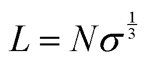
One of the main disadvantages of the grafting-to method is its inability to form very dense layers which in turn affects the thickness of the overall brush. The relationship between polymer brush thickness and its density is governed by eqn (1):
 | (1) |
We report on the effect that altering the molecular weight of the polymer PS as well as the concentration of the fabricating solution (the solution weight percentage) has on the overall brush thickness when using the grafting-to method. The polymer brushes are characterised using ellipsometry, grazing angle attenuated total reflection Fourier transform infrared spectroscopy (GA-ATR-FTIR) and atomic force microscopy (AFM) to show the thickness and quality of the films. Results show that with an increase in molecular weight gives a distinct increase in the brush thickness. Similarly, the higher solution concentrations yielded thicker brushes.
As stated, PS is one of the most widely used polymers for chemical deactivation for the use in ASD.40 Following on from the initial studies, the relationship between PS brush thickness and its ability to block a HfO2 atomic layer deposition (ALD) process was investigated. X-ray photoelectron spectroscopy (XPS) was used to determine the PS blocking efficacy. We demonstrated that the thickness had a significant effect on the brushes’ blocking capability using this process, with the thickest brush blocking what would amount to approximately 19 nm of HfO2 deposition on native Si. Our best performing polymer brush accounted for over 90% selectivity calculated using an adapted ‘selectivity equation’.41 These are comparable results to those obtained using SAMs meaning that thick PS brushes are a viable and more time efficient method for area deactivation in ASD.
Experimental
Sample preparation
Hydroxy terminated polystyrene (PS), of two molecular weights; (i) Mw = 16 kg mol−1 (16 K), polydispersity index (PDI) = 1.09 and (ii) Mw = 42 kg mol−1 (42 K), PDI = 1.06, were purchased from Polymer Source Inc. Canada, and used as received. Sample preparation was as follows: silicon substrates with native oxide of approximately 1 nm, were cleaved and degreased through ultrasonication in IPA for 30 minutes. Post sonication, the samples were hydroxy functionalised using a 3 minute O2 plasma treatment. This was performed in a Henniker Plasma HPT-200 benchtop plasma treater with an oxygen flow of 9 sccm and plasma power of 200 W. The PS was dissolved in toluene at a range of solution concentrations from 0.2 wt% to 2 wt%. These solutions were left stirring overnight at room temperature to ensure the polymer was fully dissolved. They were then spin cast onto the surface of the hydroxy functionalised silicon substrates at 3000 rpm for 30 seconds. The samples were then annealed at 200 °C for 2 h. Once annealed the samples were sonicated twice for 12 minutes in toluene to remove any ungrafted polymer chains.9 A schematic illustration of the polymer fabrication process can be seen in Fig. 1 below. | ||
| Fig. 1 Schematic diagram of polymer fabrication process. | ||
Sample characterisation
Several techniques were used in the characterisation of the polymer brushes to determine the relationship between the films’ thicknesses and the molecular weight as well as solution concentration. Ellipsometry measurements were performed to determine film thickness using a J. A. Woolam XLS-100 ellipsometer. All data analysis was performed with the CompleteEASE software using a multi-layer model. Within this model three layers were inputted, the Si substrate layer, the 1 nm SiO2 layer and finally a Cauchy model was used to determine the thickness of the PS layer. In all cases, 3 measurements were taken from different points on the sample and an average of these was calculated. The standard error of this was also calculated.GA-ATR-FTIR was performed using a Nicolet iS50 FTIR Spectrometer with a Harrick VariGATR attachment with a germanium crystal. Before sample analysis, the crystal was cleaned using butanone to remove any dust from its surface. A background scan of the atmosphere was then taken. Each sample was placed face down onto the crystal and a force of approximately 600 N was applied, this was to ensure sufficient crystal-sample contact. The sample was then scanned using unpolarised radiation at an angle of incidence of 65° for a total of 128 scans using 8 cm−1 resolution.
AFM images were obtained using a Bruker Icon AFM, using tapping mode with Tap300 Al-G tips (resonant frequency 300 kHz, force constant 40 N m−1). Image analysis and roughness calculations were then performed using Gwyddion.
To determine the blocking efficacy of the PS brushes, the films were subjected to a HfO2 ALD process. This was carried out in a custom-designed Oxford Instruments FlexAl ALD system (base pressure 5 × 10⁻⁶ Torr), which is coupled to a Scienta Omicron XPS (monochromatic Al Kα, base pressure 5 × 10⁻⁹ Torr) with a 128 channel Argus CU detector. Between the two systems there was a robotic handler arm present which remained in vacuum, which allowed for fast transfer between the ALD and XPS and for the sample to remain in vacuum.
Each PS sample was placed on a 200 mm diameter steel carrier-wafer for ALD/XPS loading and scanned using the Scienta Omicron XPS system prior to ALD treatment for comparison purposes. Once scanned the samples were transferred into the ALD system without breaking vacuum, where they were heated to 250 °C, below the polymer's degradation temperature of 260 °C.9 This temperature was chosen as it was a suitable deposition temperature for the hafnium chloride (HfCl4) precursor being used, while ensuring that the decomposition of the precursor did not occur. Once heated, the precursor was pulsed into the chamber using argon as the carrier gas with a dose time of 2 seconds. Following this, there was a 7 second purge which removed any unreacted precursor from the chamber. This was followed by a 2 second water dose. The last step was a 15 second purge. This process was repeated for 300 cycles, with the samples removed several time during the process for quasi in situ XPS analysis.
Results
Ellipsometry was performed to determine the effect that PS molecular weight and solution concentration had on the overall brush thickness. Fig. 2 shows the ellipsometry results for the polymer brushes fabricated using the 16 K and 42 K PS at different solution concentrations ranging from 0.2–2 wt%. From this figure an overall trend of increasing PS thickness with respect to solution weight percentage was observed. This relationship between thickness and weight percentage suggests that the larger number of chains in the higher concentration solutions yields denser films that allow for thicker brushes to be formed. This is due to the steric hindrance between each of the polymer chains, forcing them to elongate away from the substrate creating a thicker polymer brush.39 | ||
| Fig. 2 Ellipsometry results of average film thickness for 16 K and 42 K PS fabricated using a range of solution concentrations. Error bars signify the standard error for each of the calculated averages. | ||
From Fig. 2, the dependence of brush layer thickness on the molecular weights for each of the solution concentrations can also be ascertained. It can be seen that the brushes fabricated using the 42 K PS are generally thicker than those made with the 16 K PS. Note that for the 16 K PS there appears to be a thickness saturation at approximately 8 nm from 0.5 wt% onwards. This is compared to the thickness saturation of approximately 12 nm for the 42 K films, reached at 1.5 wt%. This variation in thickness could be due to the shorter chain length of the 16 K PS as the increase in the solution concentration made little difference to the thickness for the higher cases. Overall, from these results it can be concluded that an increase in solution concentration and molecular weight leads to a thicker polymer brush.
Once the thickness of the PS brushes was confirmed, GA-ATR-FTIR was conducted to confirm the presence of the polymer on the surface of the substrates. Fig. 3 shows the GA-ATR-FTIR spectra for the thickest films obtained for each of the molecular weights, fabricated using a 1.5 wt% solution. From these results, all peaks associated with the PS structure can be seen. These include the peaks at 292, 1450 and 900 cm−1 which correspond to the various bending and stretching modes of C–H bonds. These are mainly observed in the polymer backbone but they are also present in the benzene ring side chain. The peak at 1600 cm−1 was associated with the cyclic alkene C![[double bond, length as m-dash]](https://www.rsc.org/images/entities/char_e001.gif) C stretching modes. This is solely linked with the benzene ring and was one of the main identifiers of the PS films.42 Alongside this, the band appearing at 700 cm−1 was due to the benzene ring derivative. Both peaks confirmed the presence of the PS on the surface of the silicon, as the benzene ring was the main unique structure of the PS polymer. The final peak seen in Fig. 3 was the band appearing at 1234 cm−1 which showed the presence of C–O. This correlated to the bonds grafting the polymer to the silicon which were created in the condensation reaction forming the polymer brush.43,44
C stretching modes. This is solely linked with the benzene ring and was one of the main identifiers of the PS films.42 Alongside this, the band appearing at 700 cm−1 was due to the benzene ring derivative. Both peaks confirmed the presence of the PS on the surface of the silicon, as the benzene ring was the main unique structure of the PS polymer. The final peak seen in Fig. 3 was the band appearing at 1234 cm−1 which showed the presence of C–O. This correlated to the bonds grafting the polymer to the silicon which were created in the condensation reaction forming the polymer brush.43,44
 | ||
| Fig. 3 GA-ATR-FTIR results of the 1.5 wt% 16 K and 1.5 wt% 42 K PS as these were the thickest films obtained in each molecular weight case. | ||
Finally, AFM images were acquired to ensure that the polymer brushes fabricated were of good quality, continuous and smooth. A 1 μm × 1 μm image of the samples was obtained, and in each case the RMS roughness values were calculated. Fig. 4 shows the AFM images obtained for the thickest brushes for both molecular weights. From each image, it can be seen that the films were very smooth, and no islanding had occurred. The roughness for the 16 K PS brush was 0.2 nm and the 42 K PS brush was ∼0.3 nm. These values were extremely low and confirmed that each film was of good quality, continuous and smooth.
 | ||
| Fig. 4 AFM images of the thickest films obtained for the (a) 16 K and (b) 42 K PS samples. | ||
PS is widely known for its ability to reject metal-ion infiltration and is widely used in the ASD research field. Having gained an understanding of the dependence of brush thickness on molecular weight and solution concentration, we exposed films of a variety of thicknesses to a conventional ALD process. PS brush layers were employed to block a HfO2 ALD process, in order to understand how increasing the brush's thickness might improve the number of cycles that can be effectively blocked.40,45 Three PS brushes were fabricated with a range of thicknesses. The combinations of molecular weights and weight percentages used to achieve this range were as follows: 42 K 0.2 wt%, 16 K 0.5 wt% and 42 K 1.5 wt%. These films were evaluated using ellipsometry and had thicknesses of ∼3 nm, ∼5 nm and ∼11 nm, respectively.
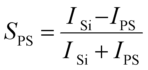
The samples were first subjected to a total of 120 cycles of the thermal HfO2 ALD process. This was carried out sequentially, with the samples moved from the ALD chamber and analysed using XPS without breaking vacuum. Using the XPS data the selectivity of each film to the ALD process was calculated using the following equation
 | (2) |
 | ||
| Fig. 5 XPS survey spectra for (a) the 42 K 1.5 wt% film, (b) the 16 K 0.5 wt% film and (c) 42 K 0.2 wt% film post Hf ALD, as well as the chemical compositions of the (d) Hf 4f, and (e) the selectivity of each of the PS films. | ||
When examining the survey spectra for each of the PS films, there was a clear increase in the Hf peak intensity on the 42 K 0.2 wt% film, this being the thinnest of the PS brushes, which can be seen in Fig. 5(c). When comparing this to Fig. 5(a) and (b), which show the two thicker PS films, there was very little contribution from the Hf peaks indicating very little deposition. This is further illustrated in Fig. 5(d), showing that the percentage Hf on the surface of the 42 K 0.2 wt% film was far greater than that on the 16 K 0.5 wt% and the 42 K 1.5 wt%. After 60 cycles of the process, the amount of HfO2 on the 42 K 0.2 wt% sample began to rapidly increase. This increase, however, did not lead to the same amount of HfO2 present on the bare Si control sample, which showed that while the thinnest sample had the weakest blocking capabilities, it still inhibited deposition to some extent. As this brush was fabricated using the same molecular weight PS as the thickest, 11 nm, sample it was determined that the molecular weight did not influence the blocking capability of the brush but it was in fact the thickness of the film that altered its efficacy. It is noted that for the Si control sample in Fig. 5(d) the percentage of Hf appears to saturate at approximately 30%. This is due to the limited sampling depth of XPS – at this point, the Si substrate is no longer detectable. Above this thickness range the intensity of the photoemission peaks associated with the deposited HfO2 layer therefore becomes constant, as there is no longer a detected substrate signal, and the newly deposited film is homogenous as a function of depth. Similar results can be observed when looking at the selectivity of these films, which can be seen in Fig. 5(e). There is a consensus in the field of ASD research that for a selective process to be successful, a selectivity of 90% or more must be achieved.14 The 16 K 0.5 wt% and the 42 K 1.5 wt% films satisfied this requirement, showing a selectivity of above 0.9 for the full range of 120 cycles. These values are comparable those demonstrated in previous works where SAMs have been used as the deactivation layer.29 As stated previously, for the two thickest films there was very little HfO2 deposited over 120 cycles. This is clear from both the XPS survey scans, as well as the contribution of Hf to the chemical compositions. From these results, it was clear that PS brushes of 5 nm and 11 nm can successfully block a Hf ALD process for a minimum of 120 cycle.
To further test the blocking efficacy, the experiment was repeated for the two thicker brushes to a total of 325 cycles. Fig. 6 shows the XPS survey scans for these two samples after the 325 cycles, as well as the Hf and selectivity percentages. From Fig. 5. it is evident that after 150 cycles there is an increase in the Hf percentage on the 16 K 0.5 wt% film. This sharp increase is very similar to what was observed in Fig. 5, as there was a relatively clear threshold number of cycles (∼40), beyond which Hf deposition began. There also is a decrease in selectivity for this brush at the point where Hf deposition begins. When looking at the thickest film (42 K 1.5 wt%), there was still very little Hf deposition observed up to 325 cycles, and as before there was no drop in selectivity below 90%. From this, it can be concluded that the 11 nm PS film can withstand a minimum of 325 cycles of Hf ALD, which represents approximately 19 nm of HfO2 on a reference silicon substrate. This was determined by taking a thickness measurement using ellipsometry of a plane silicon sample subjected to the same number of cycles. It is clear that there is a breakdown point where the film no longer blocks the ALD process and the rate at which this point is reached was dependent on the thickness of the PS brush.
 | ||
| Fig. 6 XPS survey spectra for (a) the 42 K 1.5 wt% film, and (b) the 16 K 0.5 wt% film post-ALD cycles, as well as the chemical compositions of the (c) Hf 4f, and (d) the selectivity of each of the PS films. | ||
The cause of HfO2 deposition on both the 3 nm and 5 nm films is linked to photoemission evidence of polymer breakdown. This was determined by calculating the Si2p to C1s ratio, the results of which can be seen in Fig. 7. From these results it can be seen in both cases, for the short (120 cycles) and long (325 cycles) deposition processes, that the films which allow HfO2 deposition have a large decrease in this ratio. The point at which this decrease occurs can be correlated to the point at which deposition rapidly increases, which can be seen in Fig. 5 and 6. This breakdown can also be seen in the high resolution C1s spectra, which can be seen in Fig. 8.
 | ||
| Fig. 7 C1S to Si2p ratios for the (a) short cycle and (b) long cycle process. | ||
 | ||
| Fig. 8 C1s high resolution spectra for the 42 K 1.5 wt%, 42 K 0.2 wt% brush and 16 K 0.5 wt% brush at several stages over the course of the of the HfO2 ALD process. | ||
When looking at the thickest film, the 42 K 1.5 wt% which experiences no breakdown, there is clearly no change in the spectra over the course of the ALD process. Comparing this to the 42 K 0.2 wt% and the 16 K 0.5 wt% films a clear broadening in the C1s peak can be seen as the number of ALD cycles increases. This broadening indicates an increased amount of C–O within the polymer film which shows a breakdown of the carbon backbone and benzene ring associated with the PS structure as the C–O originates from the binding of the polymer chains to the silicon substrate. This breakdown can also be seen in the O1s spectra which are shown in the ESI.† These show the increased amount of C–O present throughout the ALD process indicating polymer breakdown. It is proposed by the authors that physisorption of the HfCl4 precursor preferentially occurs in the thinner PS brushes due to their degradation. This initial physisorption thus allows for further HfO2 deposition increasing the overall oxide thickness. It is therefore concluded that a high molecular weight and wt%. brush yields thicker films of optimal area selective properties. From these results, it can be concluded that with an increase in brush thickness there is a clear increase in the blocking capability of a Hf ALD process. This result is very important in the field of ASD research because current methods used for surface deactivation which have been previously discussed, such as SAMs, have significantly longer fabrication times compared to polymer brushes. The method discussed here has the potential to be further optimised for even faster production.9
Conclusions
The controllability of brush thickness for polystyrene brush layers through the variation of molecular weight and solution concentration has been demonstrated. Firstly, the relationship between the solution concentration and thickness was illustrated for each molecular weight. Using ellipsometry it was shown that an increase in weight percentage caused an increase in thickness for all cases. The optimal weight percentage for the various molecular weights was shown to be 1.5 wt%. Secondly, the relationship between thickness and molecular weight was shown. It was seen that an increase in molecular weight also led to an increase in overall brush thickness, with 42 K PS yielding the thickest film. Finally, GA-ATR-FTIR was used to confirm the presence of each polymer on the surface of the silicon, and its bonding to the surface. AFM measurements were also conducted which showed that all films were of good quality, continuous and smooth. Following on from this investigation, the relationship between the PS brush thickness and its blocking capabilities in the case of a HfO2 ALD process were demonstrated. Using XPS, it was clear that there was a definite relationship between the thickness of the PS film and its blocking efficacy. It was seen that there was significantly less HfO2 deposition on the thickest PS films when compared to the thinnest ones. This proved that a thicker PS brushes were more effective at blocking Hf deposition than thinner films. The selectivity of these thicker brushes are comparable to those seen with SAMs, which is one of the most widely used methods for ASD. As the fabrication of SAMs can be very time consuming this similarity is a very important result for the field of ASD as the use of PS brushes is a more time efficient method of area deactivation.Conflicts of interest
There are no conflicts of interest to declare.Acknowledgements
This publication has emanated from research conducted with the financial support of Science Foundation Ireland (SFI) under Grant No. 12/RC/2278 and 16/SP/3809.Notes and references
- D. Bratton, D. Yang, J. Dai and C. K. Ober, Recent progress in high resolution lithography, Polym. Adv. Technol., 2006, 17(2), 94–103, DOI:10.1002/pat.662.
- M. A. Morris, Directed self-assembly of block copolymers for nanocircuitry fabrication, Microelectron. Eng., 2015, 132, 207–217, DOI:10.1016/j.mee.2014.08.009.
- T. Ito and S. Okazaki, Pushing the limits of lithography, Nature, 2000, 1027–1031, DOI:10.1038/35023233.
- E. Mullen and M. A. Morris, Green nanofabrication opportunities in the semiconductor industry: A life cycle perspective, Nanomater., 2021, 11, 1085–2021, DOI:10.3390/NANO11051085.
- S. O. Kim, H. H. Solak, M. P. Stoykovich, N. J. Ferrier, J. J. De Pablo and P. F. Nealey, Epitaxial self-assembly of block copolymers on lithographically defined nanopatterned substrates, Nature, 2003, 424(6947), 411–414, DOI:10.1038/nature01775.
- M. P. Stoykovich, M. Müller, S. O. Kim, H. H. Solak, E. W. Edwards, J. J. De Pablo and P. F. Nealey, materials science: Directed assembly of block copolymer blends into nonregular device-oriented structures, Science, 2005, 308(5727), 1442–1446, DOI:10.1126/science.1111041.
- D. Borah, C. Cummins, S. Rasappa, R. Senthamaraikannan, M. Salaun, M. Zelsmann, G. Liontos, K. Ntetsikas, A. Avgeropoulos and M. A. Morris, Nanopatterning via self-assembly of a lamellar-forming polystyrene-block-poly(dimethylsiloxane) diblock copolymer on topographical substrates fabricated by nanoimprint lithography, Nanomaterials, 2018, 8(1) DOI:10.3390/NANO8010032.
- T. Mårtensson, P. Carlberg, M. Borgström, L. Montelius, W. Seifert and L. Samuelson, Nanowire arrays defined by nanoimprint lithography, Nano Lett., 2004, 4(4), 699–702, DOI:10.1021/NL035100S.
- R. Lundy, P. Yadav, A. Selkirk, E. Mullen, T. Ghoshal, C. Cummins and M. A. Morris, Optimizing polymer brush coverage to develop highly coherent sub-5 Nm oxide films by ion inclusion, Chem. Mater., 2019, 31(22), 9338–9345, DOI:10.1021/acs.chemmater.9b02856.
- C. Prasittichai, K. L. Pickrahn, F. S. Minaye Hashemi, D. S. Bergsman and S. F. Bent, Improving Area-selective molecular layer deposition by selective SAM removal, ACS Appl. Mater. Interfaces, 2014, 6(20), 17831–17836, DOI:10.1021/am504441e.
- M. Fang and J. C. Ho, Area-selective atomic layer deposition: Conformal coating, subnanometer thickness control, and smart positioning, ACS Nano, 2021, 14, 58, DOI:10.1021/acsnano.5b05249.
- C. Cummins, A. P. Bell and M. A. Morris, Creating active device materials for nanoelectronics using block copolymer lithography, Nanomaterials, 2017, 7(10) DOI:10.3390/nano7100304.
- A. Sinha, D. W. Hess and C. L. Henderson, Area selective atomic layer deposition of titanium dioxide: Effect of precursor chemistry, J. Vac. Sci. Technol., B: Microelectron. Nanometer Struct. – Process., Meas., Phenom., 2006, 24, 2523, DOI:10.1116/1.2359728.
- G. N. Parsons and R. D. Clark, Area-selective deposition: Fundamentals, applications, and future outlook, Chem. Mater., 2020, 4920–4953, DOI:10.1021/acs.chemmater.0c00722.
- M. Snelgrove, C. McFeely, K. Shiel, G. Hughes, P. Yadav, C. Weiland, J. C. Woicik, P. G. Mani-Gonzalez, R. Lundy, M. A. Morris, E. McGlynn and R. O’Connor, Analysing trimethylaluminum infiltration into polymer brushes using a scalable area selective vapor phase process, Mater. Adv., 2021, 2(2), 769–781, 10.1039/d0ma00928h.
- R. Lundy, P. Yadav, N. Prochukhan, E. C. Giraud, T. F. O’mahony, A. Selkirk, E. Mullen, J. Conway, M. Turner, S. Daniels, P. G. Mani-Gonzalez, M. Snelgrove, J. Bogan, C. Mcfeely, R. O’connor, E. Mcglynn, G. Hughes, C. Cummins and M. A. Morris, Precise definition of a “monolayer point” in polymer brush films for fabricating highly coherent TiO2 thin films by vapor-phase infiltration, Langmuir, 2020, 36, 28, DOI:10.1021/acs.langmuir.0c02512.
- X. Jiang and S. F. Bent, Area-selective ald with soft lithographic methods: Using self-assembled monolayers to direct film deposition, J. Phys. Chem. C, 2009, 113(41), 17613–17625, DOI:10.1021/jp905317n.
- R. Chen, H. Kim, P. C. Mcintyre and S. F. Bent, Investigation of self-assembled monolayer resists for hafnium dioxide atomic layer deposition, Chem. Mater., 2005 DOI:10.1021/cm0486666.
- Z. Zhang, T. Dwyer, S. M. Sirard and J. G. Ekerdt, Area-selective atomic layer deposition of cobalt oxide to generate patterned cobalt films, J. Vac. Sci. Technol., A, 2019, 37, 20905, DOI:10.1116/1.5066437.
- J. O. Carlsson, Selective vapor-phase deposition on patterned substrates, Crit. Rev. Solid State Mater. Sci., 1990, 16(3), 161–212, DOI:10.1080/10408439008244628.
- J. A. Singh, N. F. W. Thissen, W. H. Kim, H. Johnson, W. M. M. Kessels, A. A. Bol, S. F. Bent and A. J. M. MacKus, Area-selective atomic layer deposition of metal oxides on noble metals through catalytic oxygen activation, Chem. Mater., 2018, 30(3), 663–670, DOI:10.1021/acs.chemmater.7b03818.
- M. F. J. Vos, S. N. Chopra, M. A. Verheijen, J. G. Ekerdt, S. Agarwal, W. M. M. Kessels and A. J. M. Mackus, Area-selective deposition of ruthenium by combining atomic layer deposition and selective etching, Chem. Mater., 2019, 31(11), 3878–3882, DOI:10.1021/acs.chemmater.9b00193.
- M. J. M. Merkx, S. Vlaanderen, T. Faraz, M. A. Verheijen, W. M. M. Kessels and A. J. M. Mackus, Area-selective atomic layer deposition of TiN using aromatic inhibitor molecules for metal/dielectric selectivity, Chem. Mater., 2020, 32(18), 7788–7795, DOI:10.1021/ACS.CHEMMATER.0C02370.
- T. G. Pattison, A. E. Hess, N. Arellano, N. Lanzillo, S. Nguyen, H. Bui, C. Rettner, H. Truong, A. Friz, T. Topuria, A. Fong, B. Hughes, A. T. Tek, A. DeSilva, R. D. Miller, G. G. Qiao and R. J. Wojtecki, Surface initiated polymer thin films for the area selective deposition and etching of metal oxides, ACS Nano, 2020, 14(4), 4276–4288, DOI:10.1021/acsnano.9b09637.
- F. S. M. Hashemi, C. Prasittichai and S. F. Bent, A new resist for area selective atomic and molecular layer deposition on metal–dielectric patterns, J. Phys. Chem. C, 2014, 118(20), 10957–10962, DOI:10.1021/JP502669F.
- R. Wojtecki, M. Mettry, N. F. F. Nathel, A. Friz, A. Silva, N. De Arellano and H. Shobha, Fifteen Nanometer resolved patterns in selective area atomic layer deposition – defectivity reduction by monolayer design, ACS Appl. Mater. Interfaces, 2018, 10(44), 38630–38637, DOI:10.1021/ACSAMI.8B13896.
- S. N. Chopra, Z. Zhang, C. Kaihlanen and J. G. Ekerdt, Selective growth of titanium nitride on HfO2 across nanolines and nanopillars, Chem. Mater., 2016, 28(14), 4928–4934, DOI:10.1021/ACS.CHEMMATER.6B01036.
- B. D. Ratner and A. S. Hoffman, Physicochemical Surface Modification of Materials Used in Medicine. In Biomaterials Science: An Introduction to Materials. 3rd edn, Elsevier Inc., 2013, pp. 259–275. DOI:10.1016/B978-0-08-087780-8.00027-9.
- D. Bobb-Semple, K. L. Nardi, N. Draeger, D. M. Hausmann and S. F. Bent, Area-selective atomic layer deposition assisted by self-assembled monolayers: A comparison of Cu, Co, W, and Ru, Chem. Mater., 2019, 31, 1635–1645, DOI:10.1021/acs.chemmater.8b04926.
- C.-W. Chang, H.-H. Hsu, C.-S. Hsu and J.-T. Chen, Achieving area-selective atomic layer deposition with fluorinated self-assembled monolayers, J. Mater. Chem. C, 2021, 9, 14589, 10.1039/d1tc04015d.
- C. de Paula, D. Bobb-Semple and S. F. Bent, Increased selectivity in area-selective ALD by combining nucleation enhancement and SAM-based inhibition, J. Mater. Res., 2021, 36(3), 582–591, DOI:10.1557/S43578-020-00013-4.
- D. Bobb-Semple, L. Zeng, I. Cordova, D. S. Bergsman, D. Nordlund and S. F. Bent, Substrate-dependent study of chain orientation and order in alkylphosphonic acid self-assembled monolayers for ALD blocking, Langmuir, 2020 DOI:10.1021/acs.langmuir.0c01974.
- M. Snelgrove, C. Zehe, R. Lundy, P. Yadav, J.-P. Rueff, R. O’Connor, J. Bogan, G. Hughes, E. McGlynn, M. Morris and P. G. Mani-Gonzalez, Surface characterization of poly-2-vinylpyridine – a polymer for area selective deposition techniques, J. Vac. Sci. Technol., A, 2019, 37(5), 050601, DOI:10.1116/1.5115769.
- M. Snelgrove, C. McFeely, P. G. Mani-Gonzalez, K. Lahtonen, R. Lundy, G. Hughes, M. Valden, E. McGlynn, P. Yadav, J. Saari, M. A. Morris and R. O’Connor, Aluminium oxide formation via atomic layer deposition using a polymer brush mediated selective infiltration approach, Appl. Surf. Sci., 2020, 515, DOI:10.1016/j.apsusc.2020.145987.
- S. T. Milner, Polymer brushes, Science, 1991, 251(4996), 905–914, DOI:10.1126/SCIENCE.251.4996.905.
- W. J. Brittain and S. Minko, A structural definition of polymer brushes, J. Polym. Sci., Part A: Polym. Chem., 2007, 45(16), 3505–3512, DOI:10.1002/pola.22180.
- B. Zdyrko and I. Luzinov, Polymer brushes by the “Grafting to” method, Macromol. Rapid Commun., 2011, 859–869, DOI:10.1002/marc.201100162.
- O. Azzaroni, Polymer brushes here, there, and everywhere: Recent advances in their practical applications and emerging opportunities in multiple research fields, J. Polym. Sci., Part A: Polym. Chem., 2012, 50(16), 3225–3258, DOI:10.1002/POLA.26119.
- P. Auroy, L. Auvray and L. Léger, Characterization of the brush regime for grafted polymer layers at the solid–liquid interface, Phys. Rev. Lett., 1991, 66(6), 719–722, DOI:10.1103/PhysRevLett.66.719.
- C. Cummins, T. Weingärtner and M. A. Morris, Enabling large-area selective deposition on metal-dielectric patterns using polymer brush deactivation, J. Phys. Chem. C, 2018, 122(26), 14698–14705, DOI:10.1021/acs.jpcc.8b04092.
- W. L. Gladfelter, Reviews selective metallization by chemical vapor deposition, Chem. Mater., 1993, 5, 1372–1388 CrossRef CAS.
- G. Socrates, Infrared and Raman characteristic group frequencies. Tables and charts, J. Raman Spectrosc., 2001, 347 Search PubMed.
- Infrared Spectroscopy Absorption Table – Chemistry LibreTexts https://chem.libretexts.org/Ancillary_Materials/Reference/Reference_Tables/Spectroscopic_Parameters/Infrared_Spectroscopy_Absorption_Table (accessed Jul 23, 2021).
- IR Spectrum Table https://www.sigmaaldrich.com/IE/en/technical-documents/technical-article/analytical-chemistry/photometry-and-reflectometry/ir-spectrum-table (accessed Jul 23, 2021).
- B. M. Coffey, E. L. Lin, P.-Y. Chen and J. G. Ekerdt, Area-selective atomic layer deposition of crystalline BaTiO3, Chem. Mater., 2019, 31(15), 5558–5565, DOI:10.1021/ACS.CHEMMATER.9B01271.
Footnote |
| † Electronic supplementary information (ESI) available. See DOI: https://doi.org/10.1039/d2tc00577h |
| This journal is © The Royal Society of Chemistry 2022 |