
 Open Access Article
 This Open Access Article is licensed under a Creative Commons Attribution-Non Commercial 3.0 Unported Licence
Electronic influence of ultrathin aluminum oxide on the transistor device performance of binary indium/tin oxide films†
M. Isabelle
Büschges
a,
Vanessa
Trouillet
b and
Jörg J.
Schneider
 *a
*a
aFachbereich Chemie, Eduard-Zintl-Institut, Fachgebiet Anorganische Chemie, Technische Universität Darmstadt, Alarich-Weiss-Straße 12, 64287 Darmstadt, Germany. E-mail: joerg.schneider@tu-darmstadt.de
bKarlsruhe Institute of Technology (KIT), Institute for Applied Materials (IAM-ESS), Hermann-von-Helmholtz-Platz 1, B 321, 76344 Eggenstein-Leopoldshafen, Germany
First published on 4th March 2022
Abstract
Heterostack thin-film transistors (TFTs) with an active layer comprising indium-, tin-, and aluminum oxide (ITAO) were fabricated using atomic layer deposition (ALD) to investigate the influence of aluminum oxide on the TFT performance parameters. Deposition of the quaternary heterostacks was accomplished at 200 °C using trimethylindium (TMI), tetrakis(dimethylamino)tin (TDMASn), trimethylaluminum (TMA), and water as oxidizing agent. By adjusting the number of Al2O3 cycles, while keeping the ratio of In2O3 to SnO2 constant, ITAO films with a well-defined Al2O3 content were obtained as confirmed by X-ray photoelectron spectroscopy (XPS). The stacked structure of the thin-films, as well as the uniform thickness was verified by high resolution transmission electron microscopy (HRTEM). The thin-film composition of the ternary ITAO semiconductors could be correlated to their electronic performance. Reducing the aluminum oxide content from three to one cycles in the atomic layer deposition experiment reveals a significant increase in the saturation mobility of nearly 300%, however at the expense of other important transistor parameters. The thus optimized ITAO thin-film exhibits a decent saturation mobility (μsat) of 2.28 cm2 V−1 s−1, a threshold-voltage (Vth) of 6.8 V, a high current on/off ratio (IOn/IOff) of 9.0 × 10⁵, and a low subthreshold swing (SS) of 365.5 mV dec−1, using a large width to length ratio (W/L = 500). Furthermore, the incorporation of aluminum oxide leads to an increase in performance stability towards exposure to background irradiation under transistor operation. The critical transistor performance parameters were altered only to a minor extent when irradiated with energies of 2.0 eV to 3.7 eV. This confirms the enhanced light stability of the TFTs, through employing a wide-band gap material as part of the semiconducting layer.
Introduction
The interest in metal oxide semiconductor thin-film transistors (TFTs) has grown in the past decades, due to an increasing demand for thin and flexible devices in display technology. They possess numerous advantages over silicon-based TFTs such as optical transparency, good device performance and low temperature processability.1 Many devices such as active-matrix liquid-crystal displays (AMLCD) and active-matrix organic light-emitting diodes (AMOLED) rely on transistors exhibiting high mobilities, high optical transparency and low processing temperatures, as well as cost.2,3 Materials comprising multinary heavy metal cations especially indium, zinc, and tin have been studied intensively for their application in TFTs. A variety of ternary and quaternary oxides, such as zinc tin oxide (ZTO),4 indium zinc oxide (IZO),5–7 and zinc indium tin oxide (ZITO)8 have emerged as promising candidates. Conventional fabrication methods for semiconducting materials include solution processing2,3,9 and sputtering.10,11 However, these methods suffer disadvantages such as uneven film thickness2 or difficulties in controlling the elemental composition.12 Recently, the method of atomic layer deposition (ALD) has shown promising results for metal oxide TFTs with comparable performance parameters. Mobility values of 6.5 cm2 V−1 s−1 up to 42.1 cm2 V−1 s−1 for multinary metal oxides, such as IZO1,6,7 and indium gallium oxide (IGO),12 as well as for single oxide TFTs,13 have been reported. ALD is a gas-phase method based on self-limiting surface reactions which enables reproducibility with a precise control over the composition and thickness of the deposited layers.6 By employing highly reactive precursor molecules, materials can be deposited at relatively low temperatures.14 Each precursor is consecutively pulsed into the reaction chamber with an inert gas being flushed between the different precursor pulses. This eliminates uncontrolled gas phase reactions and growth is limited to a maximum of one monolayer per precursor pulse. In addition, the formation of ideally pore-free layers ensures a conformal growth over large areas.13In recent years, research has concentrated on multinary metal oxide systems, although targeted efforts have been made to establish materials based on multilayered heterostructure systems of different metal oxides.6,15 The use of these heterostructures has made it possible to achieve both improved stability16 and a significant increase in the performance of metal oxide TFT components.17 By employing a stacked architecture, interfaces between the individual oxides, as well as between the substrate and the first layer of semiconducting material are generated. These interfaces exhibit special properties which have a significant influence on a multitude of electronic devices. Regardless of their importance, only limited knowledge is available about the electronic properties of most interfaces and how these are influenced by the manufacturing processes used.18 Due to the ability of growing high quality films with a high degree of homogeneity and conformality, the ALD method is a promising way to produce heterostructure-based metal oxide films with defined interfaces.7
The advantage of utilizing heterostructure stacks over single oxides is the possibility of combining the properties of the individual oxides, thus enhancing the overall performance of the component. Despite their good suitability as active channel materials, indium and zinc oxide suffer from problems regarding their long-term stability due to a limited stability against environmental influences of their respective thin-films.19 By the incorporation of suitable metal oxides, such as Al2O3, a large band gap material,18 or SnO2, with its property of being a robust channel material,8,20 this instability can be addressed.21
The material combination of In2O3 and SnO2 (ITO), with unique optical and conducting properties, has been used as a transparent conducting oxide (TCO) in transparent electrodes for the application in solar cells and flat panel displays.22 These applications demand a high carrier concentration, whereas application of transparent oxides in transistor devices require semiconducting materials with a controllable carrier concentration.23 An efficient method for controlling the overall conductivity of the material is to incorporate an ion which is able to reduce the concentration of free electrons, viz. the charge carrier concentration. For this purpose, gallium oxide is often used in semiconducting materials. The strong Ga–O bond suppresses the formation of oxygen defects and the associated generation of mobile electrons.23 As an alternative aluminum oxide can be employed, as it also possesses a strong metal–oxygen bond, however, due to its high dielectric constant (∼9),24 Al2O3 is often used as dielectric in TFT devices.25 Despite these properties, Al2O3 in combination with ZnO has been reported as an active semiconductor layer realizing high-performance TFTs with a mobility of 27.8 cm2 V−1 s−1.25 Furthermore, due to its large band gap of 8.7 eV,24 an improved stability under illumination is expected in corresponding TFTs.
The combination of In2O3, Al2O3, and SnO2 in a quaternary heterostructure is a promising material combination to study the influence of a wide band gap oxide like aluminum oxide with a large oxophilicity on the semiconducting properties of a thin-film metal oxide combination in a TFT device.26 Such studies are meaningful in order to gain a further understanding on the influence and control-mechanisms of oxygen vacancies (VO) which are responsible for the charge conduction in thin-film oxide semiconductors.27–29
Herein, we have investigated the influence of aluminum oxide doping on binary thin-film heterostructures composed of In2O3 and SnO2. We have studied its influence on the TFT performance parameters of the indium oxide/tin oxide semiconducting layer structure, and have determined the conduction mechanism responsible for the transistor performance characteristics. In addition, we studied the performance of the thin-film transistors under illumination conditions and determined their respective characteristics.
Results and discussion
Fabrication and characterization of the ternary heterostack structures
To fabricate the desired heterostacks comprising of In2O3, SnO2, and Al2O3 the individual oxides were deposited via ALD with a constant number of cycles for In2O3 and SnO2. However, the number of Al2O3 cycles was varied between one and three to investigate the influence of the wide band gap oxide Al2O3 on the TFT performance parameters of the layered In2O3/SnO2 composition. The deposition of these three oxides consecutively forming the metal oxide heterostack is referred to as an ALD supercycle. By repetition of a supercycle the total film thickness can be controlled. A schematic representation of the deposition process for one supercycle is shown in Fig. 1. The first part of the supercycle consists of the exposure of the substrate to a TMI pulse for a certain exposure period and the consequent oxidation with water. In the first step TMI molecules react with surface OH-groups of the substrate (step 1). Following an exposure time, the reactor is purged with argon to remove remaining precursor molecules and gaseous side products. Subsequently an oxidizing agent in the form of water is introduced into the reaction chamber for an extended exposure time, thereby allowing OH-groups to be formed (step 2). After purging the reactor with argon, the sequence is repeated to obtain the desired thickness of the In2O3 film (step 3). SnO2 and Al2O3 are deposited from TDMASn (steps 4–6) and TMA (steps 7–9), respectively, and oxidized with water in the same manner as described for In2O3. The sequence of depositing the three individual oxides on top of each other is described as supercycle. It enables the fabrication of a heterostack with a precise control over the film thickness of each single oxide. By reiterating the full supercycle the total film thickness can be controlled.30 The exact deposition parameters for each precursor is given in the experimental section. The investigated heterostacks comprise of 26 cycles In2O3, 15 cycles SnO2, which are modified with one to three cycles of Al2O3 deposited in eight supercycles (see caption of Fig. 1 for sample denomination).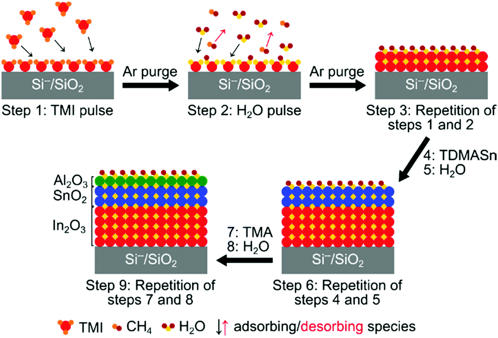 | ||
Fig. 1 Schematic diagram of the ALD process to fabricate In2O3/SnO2/Al2O3 (ITAO) heterostructure stacks. The deposition of In2O3 from TMI and water is depicted in detail (step 1–3). In step 1 TMI reacts with surface OH groups of the substrate, an argon purge flushes unreacted molecules from the reactor. A subsequent water pulse reacts to form OH groups on the surface and CH4 as by-product (step 2). A final argon purge removes the by-products and unreacted molecules. The layer thickness of the In2O3 can be adjusted by repeating steps 1 and 2 (step 3). In the same manner, SnO2 and Al2O3 are deposited from TDMASn (steps 4–6) and TMA (steps 7–9), respectively. Thin-films prepared within this work exhibit a composition of In2O3/SnO2/Al2O3 26![[thin space (1/6-em)]](https://www.rsc.org/images/entities/char_2009.gif) :15:1 (ITAO 1), 26:15:2 (ITAO 2), and 26:15:3 (ITAO 3), deposited in eight supercycles. :15:1 (ITAO 1), 26:15:2 (ITAO 2), and 26:15:3 (ITAO 3), deposited in eight supercycles. | ||
The composition of the heterostructure stacks was investigated with UV-vis measurements, high resolution transmission electron microscopy (HRTEM), and X-ray photoelectron spectroscopy (XPS). Finally, to evaluate the semiconducting properties with respect to the influence of the aluminum oxide content, thin-film transistor devices were fabricated.
Thin-film characterization
To clarify the thin-film architecture of the deposited heterostructures cross-sectional high resolution transmission electron microscopy (HRTEM) was performed. Micrographs of sample ITAO 2 revealed a uniform film thickness of ∼15 nm with an excellent homogeneity over a large area of the deposited film (Fig. 2a). Distinct layers with lighter and darker contrast are observable, which can be assigned to In2O3 and SnO2, respectively, revealing a layered architecture of the film (Fig. 2b) with a composition In2O3/SnO2/Al2O3 of 26:15:2 deposited over eight supercycles. Due to the exceeding larger number of layers originating from In2O3 and SnO2, individual Al2O3 layers cannot be observed in the HRTEM images. However, the number of assignable layers is in accordance with the number of supercycles.
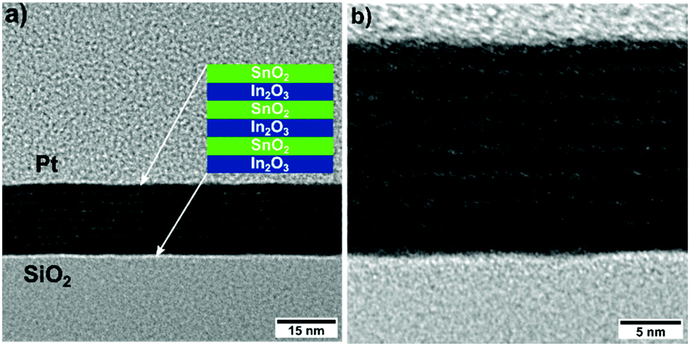 | ||
| Fig. 2 Cross-sectional HRTEM micrographs obtained via focused ion beam (FIB) sample preparation of the thin-film ITAO 2 with the composition In2O3/SnO2/Al2O3 26:15:2. The homogenous nature of the film over a large area (a) can be observed as well as a layered architecture of the heterostack (b). Layers with lighter contrast can be attributed to In2O3, while those with darker contrast can be assigned to SnO2. | ||
The elemental composition of the three heterostack architectures ITAO 1–3 with varying Al2O3 amount was investigated by X-ray photoelectron spectroscopy (XPS). The peaks for the individual Al 2p core level spectra are located at 73.9 eV for Al 2p3/2 and 74.5 eV for Al 2p1/2, with no significant peak shifts (Fig. 3a) with respect to the increasing Al content in the stacks moving from ITAO 1–3.18,31 As expected from the compositional differences of the thin-films, the Al concentration increases with the increasing number of Al2O3 deposition cycles, from 8.5 at% to 14.5 at%. As the oxygen-related species exert a strong influence on the performance parameters of a TFT,3,6 the investigation of the O 1s core level is intriguing. The O 1s core level (Fig. 3b) is deconvoluted into three peaks, which can be assigned to different oxygen species present within the thin-film. At lower binding energies, the peaks can be assigned to fully coordinated oxygen (Mx–Oy) species,3 related to In2O3 und SnO2 at 530.1 eV and Al2O3 at 531.5 eV,32,33 respectively. The latter peak might also contain additional contributions from defect rich Mx–Oy species, associated with VO vacancies in the oxygen lattice.34 Contributions of surface and bulk OH groups in the films, and probably carbonate species (due to very similar binding energies, contributions from hydroxyl and carbonate species are not clearly distinguishable33,35) are represented by the peak at higher binding energies of 532.6 eV.3,33 As evident from the Al 2p core level, the peak at 531.5 eV also shows an increase with the increasing incorporation of Al3+ in the heterostructures of ITAO 1, 2, and 3, while the Mx–Oy contributions from In2O3 and SnO2 decrease from 43.2 to 31.7 at%, accordingly (Table 1). This fact clearly indicated the doping of Al3+ into the In2O3/SnO2 layer, which reflects the high affinity of aluminum towards oxygen.28 Simultaneously the concentration of M–OH increases. The Sn 3d5/2 core level peak (Fig. 3c) positioned at 486.6 eV together with the maximum of the valence band at 4.7 eV (Fig. S1b, ESI†) demonstrate the presence of SnO2.36 The In 3d5/2 core level peak located at 444.5 eV (Fig. 3d) and the In MNN Auger line (Fig. S1a, ESI†) indicate unambiguously the presence of In2O3.37
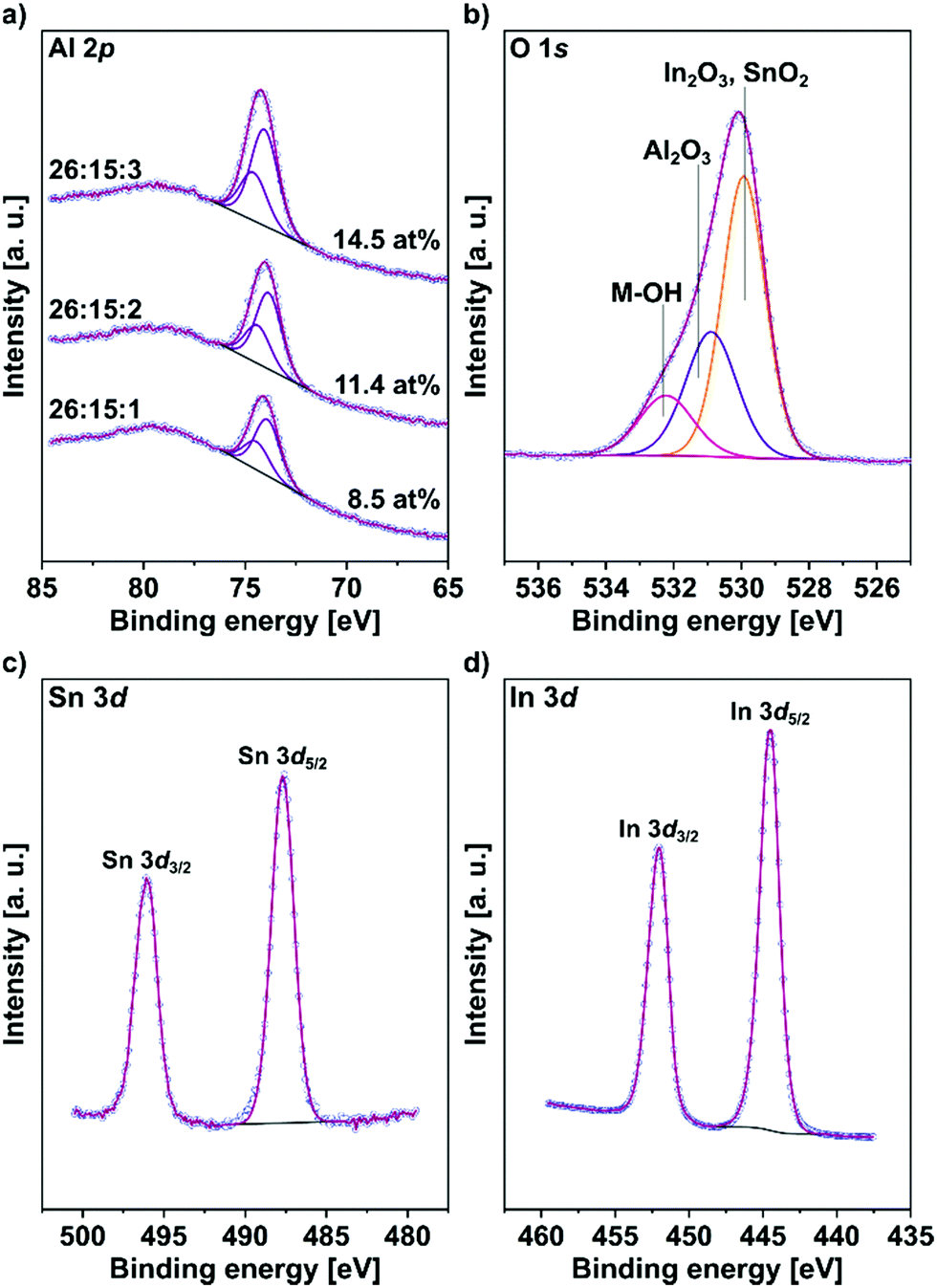 | ||
| Fig. 3 XPS core level spectra of the heterostructure stack ITAO 2 for (a) Al 2p, (b) O 1s, (c) Sn 3d, and (d) In 3d. All spectra were referenced to the C 1s peak at 285 eV. The respective core level for ITAO 1 and ITAO 3 exhibit similar BE values and are reported in Table S1 (ESI†). | ||
| Composition In2O3/SnO2/Al2O3 | Mx–Oy In2O3, SnO2 atom% | Mx–Oy Al2O3 atom% | M–OH atom% |
|---|---|---|---|
| 26:15:1 ITAO 1 |
43.2 | 9.7 | 2.9 |
| 26:15:2 ITAO 2 |
39.2 | 10.2 | 5.4 |
| 26:15:3 ITAO 3 |
31.7 | 16.1 | 8.8 |
The optical properties of the thin-films ITAO 1–3 were investigated though UV-vis measurements. All ITAO thin-films show an optical transparency above 85% in the visible region as indicated in Fig. 4a. From the transmission data Tauc plots (Fig. 4b) were generated to determine the optical band gaps of the thin-films.38
 | ||
| Fig. 4 Optical properties and Tauc plot of the three heterostructures ITAO 1–3 (red, blue, green). | ||
The Tauc plots of the three thin-films differ only to a minor, but nevertheless significant, extent. Interestingly, the band gap widens from 3.08 to 3.15 eV observable even with a subtle increase in the number of aluminum oxide deposition cycles from one to three (Table 2). Obviously, by introducing the wide-band gap material aluminum oxide (Eg = 7.0 eV)39 into the semiconducting In/Sn oxide heterostack, the band gap of the ternary ITAO films is affected considerably. This is in accordance with very recent work on the plasma enhanced ALD synthesis of indium oxide/aluminum oxide binary layers, in which a similar increase with an increase of the Al3+ incorporation is observed.28
| Composition In2O3/SnO2/Al2O3 | Band gap [eV] |
|---|---|
| 26:15:1 ITAO 1 |
3.08 |
| 26:15:2 ITAO 2 |
3.12 |
| 26:15:3 ITAO 3 |
3.15 |
Thin-film device integration of the heterostacks ITAO 1–3 and determination of the conduction pathway
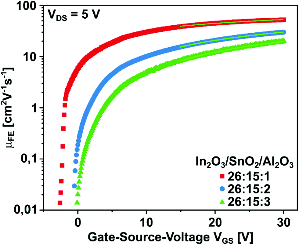
Finally, the ITAO heterostack thin-films were integrated into TFT devices to study the influence of aluminum oxide on the transistor performance of the indium/tin oxide semiconductor stack. As Al2O3 is a dielectric material with a strong metal–oxygen bond, a notable suppression of the density of free charge carriers could be expected.29 In addition, the incorporation of a material such as aluminum oxide, with a significantly larger band gap, compared to In2O3 and SnO2, can lead to an increase in performance stability towards exposure to background irradiation under transistor operation. In order to verify this hypothesis, in addition to the examination of the transistor performance parameters under exclusion of light, the behavior of these parameters under irradiation with light of different wavelengths was examined. Due to the strength of the Al–O bond and the large band gap, the fraction of aluminum oxide in the ITAO films was kept low and was varied only to a small extent. The IV characteristics of the fabricated transistors were thus subsequently studied. From the transfer and output curves (Fig. 5), the characteristic TFT parameters (Table 3) were extracted to allow the comparison of heterostructures with different compositions. | ||
| Fig. 5 (a) Collective transfer characteristics of the TFT with one, two, and three cycles Al2O3 ITAO 1–3 (red, blue, green) and (b–d) the corresponding output characteristics of the In2O3/Al2O3/SnO2 heterostructures ITAO 1–3, at different gate–source voltages, respectively. | ||
| Composition In2O3/SnO2/Al2O3 | Mobility, μsat [cm2 V−1 s−1] | On-voltage, VOn [V] | Threshold voltage, Vth [V] | Current on/off ratio, IOn/IOff | Subthreshold swing, SS [mV dec−1] |
|---|---|---|---|---|---|
| 26:15:1 ITAO 1 |
4.87 | −2.8 | 3.2 | 4.7 × 10⁴ | 631.0 |
| 26:15:2 ITAO 2 |
2.28 | −0.9 | 6.8 | 9.0 × 10⁵ | 365.5 |
| 26:15:3 ITAO 3 |
1.37 | −0.7 | 8.1 | 3.6 × 10⁶ | 388.5 |
By reducing the aluminum oxide content from two to one deposition cycles, the conductivity of the semiconductor layer is increased. This can be observed in the transfer curve of the TFT ITAO 1 (26:15:1) due to the higher currents in the on and off state (Fig. 5a), as well as in the corresponding output curve (Fig. 5b), while increasing the Al2O3 content to three deposition cycles leads to a reduction in conductivity (Fig. 5a and d). The TFT performance parameters of the three transistors are summarized in Table 3.
With respect to the charge carrier mobility μ, reducing the Al2O3 content from two to one cycle leads to a significant mobility increase from 2.28 cm2 V−1 s−1 to 4.87 cm2 V−1 s−1, while the threshold voltage is reduced to 3.2 V. Due to the significant increase of the off current with only a moderate increase of the on current, the current on/off ratio (IOn/IOff) is lowered one order of magnitude compared to transistor ITAO 2, while the subthreshold swing in increased to 631 mV dec−1. The subthreshold swing is directly related to the density of traps at the interface between dielectric and semiconductor.16 Lower SS values for ITAO 2 indicate a decreased trap density compared to ITAO 1, which is also in agreement with the property of Al to suppress oxygen defects effectively.40 A further increase of the Al2O3 content up to three deposition cycles reduces the mobility further to 1.37 cm2 V−1 s−1, accompanied with a higher Vth of 8.1 V. However, while the on current is slightly reduced, the off current is lowered to a significant extent, leading to an increased IOn/IOff of 3.6 × 10⁶. Investigations of an ITO/Al2O3 interface by XPS revealed that by increasing the Al2O3 film thickness up to a certain value, the position of the Fermi level (EF) of the binary structure in lowered.18 Therefore the difference between EF and the conduction band minimum (CBM) increases, leading to significantly fewer subgap states being filled. These act as trap states with respect to charge carriers, hence influencing the charge transport and consequently the charge carrier mobility.11
Despite the attractive mobility and relatively low Vth, the single Al2O3 cycle TFT (ITAO 1) exhibits an elevated off-current (Fig. 5b). However, the off-current should be as low as possible for an efficient transistor to consume as little energy as possible in the off state. The offcurrent can be significantly reduced by increasing the Al2O3 content up to three deposition cycles, but this is accompanied by a trade off in the charge carrier mobility. In order to further optimize the TFT parameters with respect to a varying layer composition, different doping levels of wide band gap dopants into such binary semiconductor combinations have to be studied. The optimized value of the saturation mobility of 2.28 cm2 V−1 s−1 for ITAO 2 falls within the range of previous reports of TFT device structures comprising of amorphous indium gallium oxide as active channel layer, deposited via ALD, with mobilities of 0.17 cm2 V−1 s−1 up to 9.45 cm2 V−1 s−1, depending on the individual fabrication conditions chosen.12 However, in addition to the mobility, the subthreshold swing is also an important performance parameter. The TFT ITAO 2 shows a subthreshold swing of 365.5 mV dec−1, thus falling in the range of recently reported IGO-TFTs (260–420 mV dec−1)12 and that of polycrystalline In2O3/ZnO-TFTs, with reported values between 162 mV dec−1 and 621 mV dec−1.6 The density of free charge carriers, nfree, can be calculated directly from the measured drain-current, IDS, employing the following equation11

For the thin-films ITAO 1–3 values for the charge carrier density nfree were obtained ranging from 2.01 × 1016 cm−3 to 3.74 × 1016 cm−3 (for details see ESI†). These values are in accord with nfree obtained for a-IGZO with values ranging from 1017 to 1020 cm−341 and Ti-doped ITO with nfree ∼ 1017 cm−3.42
The conduction path of mobile electrons in TFT devices based on an active layer of metal oxides can be best understood by a percolation conduction (PC) or a trap-limited conduction (TLC) pathway. In the former a distribution of potential barriers is present within the conduction band. The mobile electrons as charge carriers move around these barriers, finding the path of least resistance.23 Whereas in the TLC mode charge carriers are being trapped in tail states and are statistically released over time.43 A schematic representation of the two conduction mechanisms is depicted in Fig. 6.
 | ||
| Fig. 6 Illustration of the (a) percolation conduction mechanism (PC) and the (b) trap-limited conduction mechanism (TLC). In (a) a distribution of potential barriers is shown, around which an electron ‘e’ moves taking the path of least resistance, whereas in (b) localized tail states hinder the path of a mobile electron by multiple trapping and releasing events. | ||
Along with the density of tail states (Ntc), the position of the Fermi level (EF) is decisive for the prevalent type of conduction mechanism. If FE is located within the localized tail states and thus below the CBM (EF ≪ EC), these tail states act as traps whereby the charge transport is dominated by TLC. Here the field effect mobility μFE is proportional to nfree/(nfree + ntrap), with nfree/ntrap − density of free/trapped charge carriers, where n is the number of charge carriers.43 However, if the Fermi level is at or above the CBM, the tail states are prefilled and μFE is dominated by PC. Thus, a band-like charge transport occurs, which is only influenced by the height and width of the potential barriers within the conduction band.43 At higher temperatures the electrons take a shorter conduction path, which increases the mobility and reduces the activation energy.23
To determine the prevalent charge transport mechanism of the deposited heterostacks ITAO 1–3, the dependency of the field-effect mobility (μFE) on the gate voltage was investigated (Fig. 7) and fitted with the power law

 | ||
| Fig. 7 Field-effect mobility (μFE) dependence on the gate voltage and their corresponding power-law fits for ITAO 1–3 (red, blue, green). | ||
| Composition In2O3/SnO2/Al2O3 | γ | Mobility μFE [cm2 V−1 s−1] | Conduction mechanism |
|---|---|---|---|
| 26:15:1 ITAO 1 |
0.40 | 4.87 | TLC |
| 26:15:2 ITAO 2 |
0.73 | 2.28 | TLC |
| 26:15:3 ITAO 3 |
0.87 | 1.37 | TLC |
The values for γ indicate that when reducing the aluminum oxide content from three deposition cycles to one, the conduction mechanism shifts from a TLC dominated to a transitional region, indicating no clear distinction between TLC and PC pathways. In contrast, for the heterostacks with two and three deposition cycles Al2O3 (ITAO 2 and ITAO 3), γ exhibits values of 0.73 and 0.87, respectively. These indicate a charge carrier transport clearly dominated by the TLC mechanism. This fact might explain the decreased values of the corresponding mobilities with 2.28 cm2 V−1 s−1 and 1.37 cm2 V−1 s−1 for ITAO 2 and ITAO 3, respectively. For ITAO 1, with a γ value of 0.40, it can be assumed that the conduction mechanism is shifted towards PC dominated, which is also reflected in the considerably higher mobility of 4.87 cm2 V−1 s−1. Since the predominant charge transport mechanism is generally influenced by the density of tail states (Ntc) near the conduction band edge,43 the decrease of the exponent indicates a reduction of these states for ITAO 1 and being responsible for the increased mobility value. When the Fermi level EF is shifted towards higher energies and thus raised closer to the CBM, tail states are being filled, which significantly reduces the limitations on the charge transport.43 In contrast, a high density of these states located near the CBM leads to Fermi level pinning.43 Meaning EF cannot be raised above the CBM by applying a large drain voltage and charge transport is controlled by trap and release events of charge carriers, and therefore described by TLC.43
In order to investigate these findings in more depth, a study of the temperature dependence of the charge carrier mobility is advisable and could further discriminate between the two charge transport mechanisms TLC and PC.6,44 For the former, temperature dependency is observed, whereas the PC conduction mechanism is described as temperature-independent.41,43 This is due to the dependence of the activation energy on the density of free charge carriers, which is continuously reduced with increasing carrier density.44 To elucidate the temperature dependence of the mobility, low-temperature measurements were performed. In Fig. 8 the mobility values of the transistors are logarithmically plotted against the inverse temperature 1000/T in an Arrhenius plot.
 | ||
| Fig. 8 Arrhenius plots of the transistors ITAO 1–3 (red, blue, green) displaying the temperature dependence of the saturation mobility in the range between room temperature and 123 K. | ||
The Arrhenius plot shows that the mobility of the investigated transistors decreases with decreasing temperature. This temperature dependence of the mobility is also reflected in the values of the corresponding temperatures summarized in Table 5.
| Temperature [K] | 26:15:1 ITAO 1 |
26:15:2 ITAO 2 |
26:15:3 ITAO 3 |
|---|---|---|---|
| Mobility μsat [cm2 V−1 s−1] | |||
| 295 | 4.85 | 2.28 | 1.32 |
| 273 | 3.76 | 2.11 | 1.18 |
| 248 | 4.00 | 1.95 | 1.12 |
| 223 | 3.65 | 1.68 | 0.95 |
| 198 | 3.52 | 1.54 | 0.70 |
| 173 | 3.43 | 1.32 | 0.68 |
| 148 | 2.99 | 1.14 | 0.57 |
| 123 | 2.64 | 1.02 | 0.41 |
The Arrhenius plot as well as the mobility values show a temperature dependency which becomes more pronounced as the Al2O3 content increases. In determining the charge transport mechanism, it was assumed that the TFT with only one deposition cycle of Al2O3 is situated in a transition region between TLC and PC mechanism. This assumption can be confirmed by the low temperature measurement. While the TFT ITAO 1 shows a decline in mobility of only 46%, with a value of 4.85 cm2 V−1 s−1 at T = 295 K decreasing to 2.64 cm2 V−1 s−1 at T = 123 K, the TFT ITAO 2 displays a slightly greater decrease of 55%. In contrast, the transistor with three cycles of Al2O3 shows a significantly greater dependency with a drop in mobility of 69% from 1.32 cm2 V−1 s−1 at T = 295 K to 0.41 cm2 V−1 s−1 at T = 123 K. This strong temperature dependency of the TFT ITAO 3 confirms the previous assumption of the predominant transport mechanism for this transistor being best described by the TLC mechanism.
TFT performance of the heterostacks ITAO 1–3 under illumination
The behavior of the TFT performance parameters under the influence of illumination was also investigated. IV measurements were carried out, while the transistor devices were simultaneously exposed to LED light sources with different energies, ranging from 2.0 eV to 3.7 eV (for the setup see Fig. S3, ESI†) As a reference, IV measurements were performed in the dark. Between the transistor measurements and the illumination experiments, the TFTs were stored under dark conditions at a constant temperature of 22 °C. In Fig. 9 the evolution of the transfer curves with increasing energy of illumination is shown for the three transistors.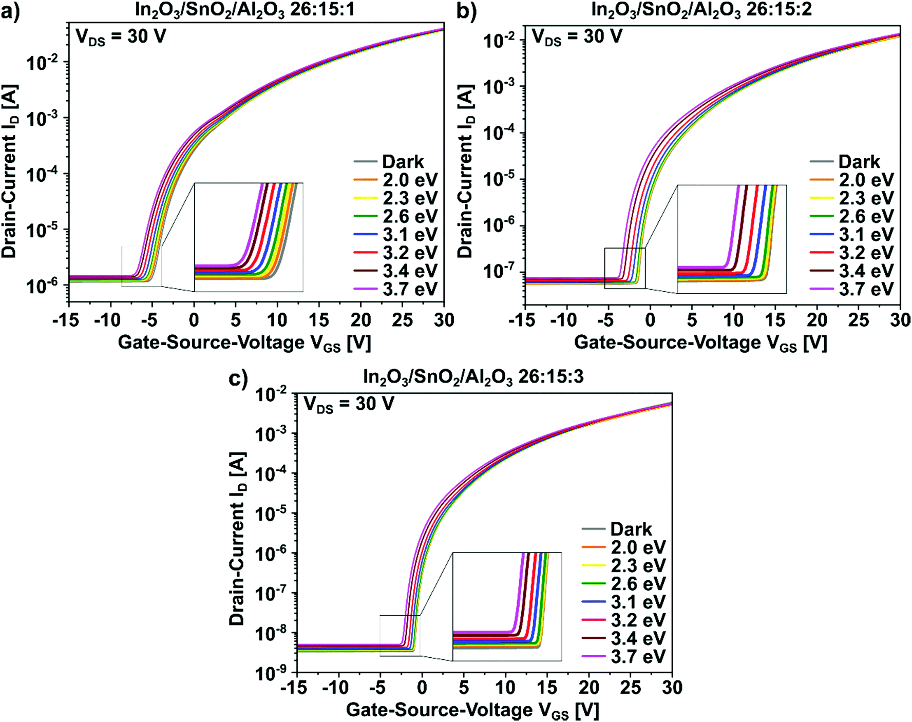 | ||
| Fig. 9 Collective transfer characteristics of the individual ITAO heterostacks under illumination for the devices with the composition In2O3/Al2O3/SnO2 (a) 26:15:1, (b) 26:15:2, and (c) 26:15:3. | ||
The transfer curves for the three transistors with different Al2O3 contents (Fig. 9) show an increase in IOff and a negative shift of VOn with increasing energy of illumination. From the data shown in Table 6 the difference between the three compositions becomes more evident. The transistor ITAO 1 (one deposition cycle of Al2O3) shows a clear negative shift of VOn of 2.2 V when illuminated with an energy of 3.7 eV, with an increase of IOff by a value of 4.0 × 10⁻⁷ A. In comparison, the values for ITAO 3 (three deposition cycles of Al2O3) only shift by 1.3 V for VOn and 1.7 × 10⁻⁹ A for IOff, respectively. The reduced shift of the two parameters indicates a higher stability under illumination for the transistor with three deposition cycles of Al2O3, which can be attributed to a broadened band gap, as shown in Fig. 4b and listed in Table 2. From the data (Table S3, ESI†) it is also evident, that for transistor ITAO 3, a more pronounced shift of VOn occurs at an energy of 3.1 eV, which falls within the energy range of the respective band gap of 3.15 eV. This indicates that for the TFT with three deposition cycles of Al2O3 photons of a higher energy are needed to generate a sufficient amount of charge carriers in the semiconducting channel for it to be conducting. The phenomenon of a simultaneously increased on- and off-current with increasing energy of irradiation and thus a decreased IOn/IOff can be explained by persistent photoconductivity (PPC).27 This is caused by inducing charge carriers into the semiconducting channel through irradiation. The phenomenon is more evident in the off- than in the on-state of the transistor. When in the on-state, the channel already possesses a high density of free charge carriers and inducing more carriers only leads to a minor increase in conductivity. However, when in the off-state, the semiconducting channel is deprived of charge carriers, hence inducing a certain amount of charge carriers though irradiation results in a more drastic increase in conductivity (rising IOff) in comparison.45 A negative shift of the threshold-voltage, and also VOn, can be attributed to photo-generated charge trapping in the dielectric.46,47 Thereby the charge density in the semiconducting channel, as well as in the dielectric and their interface is influenced.47 Comparing these results with those of transparent ZTO and IZO TFTs,6,47 a significantly improved stability of the TFT parameters under illumination is observed in the TFT in which Al2O3 is incorporated into the semiconducting layer (ITAO 1–3). In comparison with a-IGZO TFTs,46 in which a similar effect can be expected because of its comparably large band gap of ∼3.2 eV48 and due to the properties of Ga, which is utilized to suppress the generation of charge carriers,16 it could be demonstrated herein that the use of Al2O3 leads to a significantly smaller change in the critical parameters under irradiation.
| Heterostructure In2O3/SnO2/Al2O3 | Mobility μsat [cm2 V−1 s−1] | On-voltage VOn [V] | Threshold-voltage Vth [V] | Off-current IOff [A] | Current on/off ratio IOn/IOff | Subthreshold swing SS [mV dec−1] | ||||||
|---|---|---|---|---|---|---|---|---|---|---|---|---|
| Dark | 3.7 eV | Dark | 3.7 eV | Dark | 3.7 eV | Dark | 3.7 eV | Dark | 3.7 eV | Dark | 3.7 eV | |
| 26:15:1 ITAO 1 |
5.07 | 4.95 | −5.4 | −7.6 | 1.9 | 0.3 | 1.1 × 10⁻⁶ | 1.5 × 10⁻⁶ | 3.1 × 10⁴ | 2.6 × 10⁴ | 1357 | 1471 |
| 26:15:2 ITAO 2 |
2.42 | 2.12 | −1.7 | −4.0 | 6.4 | 3.6 | 5.5 × 10⁻⁸ | 7.6 × 10⁻⁸ | 2.2 × 10⁵ | 1.6 × 10⁵ | 598 | 728 |
| 26:15:3 ITAO 3 |
1.29 | 1.02 | −1.1 | −2.4 | 7.8 | 5.8 | 3.3 × 10⁻⁹ | 5.0 × 10⁻⁹ | 1.8 × 10⁶ | 9.6 × 10⁵ | 406 | 501 |
Our investigations reveal that an increased stability under illumination can be achieved when employing a modest quantity of Al2O3 as a component to tune the composition of the semiconducting layer in a most effective manner.
Conclusions
ALD derived heterostacks comprising In2O3, SnO2, and Al2O3 were fabricated at 200 °C using trimethylindium, tetrakis(dimethylamino)tin, and trimethylaluminum as metal precursors and water as an oxidizing agent. The possibility of a layer-by-layer deposition allows a precise control over the composition and therefore over the thickness of each individual metal oxide, resulting in a heterostructure stack with well-defined and tunable properties. The material characterization revealed a high optical transparency in the visible region as well as a broadening of the thin-film's band gap with increasing Al2O3 content. To study the influence of the Al2O3 on the thin-film performance parameters the In2O3/SnO2/Al2O3 heterostacks were integrated into TFT devices. Fabricated devices with an optimized composition of 26:15:2 (In2O3/SnO2/Al2O3) demonstrated an average saturation mobility (μsat) of 2.28 cm2 V−1 s−1, a threshold voltage (Vth) of 6.8 V, a current on/off ratio (IOn/IOff) of 9.0 × 10⁵, and a subthreshold swing (SS) of 365 mV dec−1 at a postdeposition annealing temperature of 400 °C. Additionally, the alteration of the TFT performance parameters under the influence of illumination with light of varying wavelength was studied. By using Al2O3 as part of the semiconducting layer, an increased stability under illumination could be achieved. The improvement was expressed by a maintained semiconducting behavior, evident from the transfer curves, with only a minor increase in off-current (IOff) and a slight negative offset (VOn) of the curves. Altogether, our investigations revealed the possibility of tuning the semiconducting properties of thin-films by adding ultrathin layers or rather a relatively modest number of deposition cycles of a wide band gap material in a precise manner as doping material, thereby controlling the interfacial charge transport mechanism. The resulting heterostack structures can lead to intriguing applications in TFT devices and further open the door to sophisticated modifications of functional thin layer device structures.
Experimental
Fabrication of the ITAO 1–3 heterostacks by ALD
The fabrication of the In2O3/SnO2/Al2O3 heterostructures was carried out using a Savannah S 100 system (Cambridge Ultratech). The deposition process was performed at 200 °C with a base pressure of 3.0 torr. Prior to the deposition the substrates were kept inside the ALD chamber for 20 min at 200 °C under an argon flow of 20 sccm. As precursors for the metal oxides trimethylindium (99.999%, AkzoNobel), trimethylaluminum (min. 98%, AkzoNobel), and tetrakis (dimethylamido)tin49 were used for In2O3, Al2O3, and SnO2, respectively. Water (HPLC grade, Sigma Aldrich) was used as an oxidant. The precursors including the oxidant were kept at room temperature, except for the tin precursor which was heated to 60 °C. Argon (99.9999%, Alpha Gaz™) was used as carrier gas for the deposition and set to a constant flow rate of 20 sccm. The deposition parameters for In2O3 were: TMI pulse 0.1 s, exposition 1.5 s, argon purge 20 s, H2O pulse 0.1 s, exposition 1.5 s, argon purge 20 s. The sequence for SnO2 was: TDMASn pulse 0.5 s, exposition 1.5 s, argon purge 30 s, H2O pulse 0.015 s, exposition 1.5 s, argon purge 30 s. For Al2O3 the sequence used was: TMA pulse 0.015 s, exposition 1.5 s, argon purge 30 s, H2O pulse 0.015 s, exposition 1.5 s, argon purge 15 s. The variation of the composition was regulated by the number of cycles of a single oxide. The number of Al2O3 cycles was varied between one and three, while the number of cycles for In2O3 and SnO2 were kept constant at 26 and 15, respectively. To increase the overall film thickness the consecutive deposition of the single oxides was repeated eight times via ALD supercycles.Material characterization of the ITAO 1–3 heterostacks
UV-vis measurements were performed on quartz substrates (15 × 15 mm2) with an Evolution 600 spectrometer (Thermo Scientific) with wavelengths ranging from 190–900 nm. Film thicknesses were obtained by ellipsometry on coated Si/SiO2 substrates using a spectroscopic ellipsometer M2000 (J.A. Woollam) in a spectral range of 370–1690 nm and an angular range of 45–85°. High resolution transmission electron microscopy (HRTEM) was performed using a FEI Tecnai G2 F20 with an operating voltage of 200 keV.50 Samples for the TEM investigations were prepared by ALD deposition on TFT substrates (15 × 15 mm2) which were annealed at 400 °C for 40 minutes and electrical characterized before the TEM measurements. Samples for focused ion beam (FIB) were prepared using a gallium-focused ion beam (FEI Helios NanoLab 460F1 FIB-SEM) and a subsequent coating with a platinum layer.51 XPS measurements were performed using a K-Alpha+ XPS spectrometer (ThermoFisher Scientific, East Grinstead, UK). Data acquisition and processing using the Thermo Avantage software is described elsewhere.52 All samples were analyzed using a microfocused, monochromated Al Kα X-ray source (400 μm spot size). The K-Alpha+ charge compensation system was employed during analysis, using electrons of 8 eV energy, and low-energy argon ions to prevent any localized charge build-up. The spectra were fitted with one or more Voigt profiles (BE uncertainty: +0.2 eV) and Scofield sensitivity factors were applied for quantification.53 All spectra were referenced to the C 1s peak (C–C, C–H) at 285.0 eV binding energy controlled by means of the well-known photoelectron peaks of metallic Cu, Ag, and Au, respectively. Samples for the XPS investigation were prepared by thin-film deposition on Si/SiO2 substrates (10 × 10 mm2) and annealed at 400 °C for 40 minutes.Thin-film transistor characterization
For TFT characterization commercial substrates (Fraunhofer IMPS, Dresden) with prefabricated source–drain electrodes in a bottom-gate-bottom-contact (BGBC) device geometry were used. The substrates consist of highly n-doped silicon (gate electrode) with a 90 nm silicon oxide dielectric layer. The source–drain electrodes are employed as an interdigital structure, with a channel length of L = 20 μm and width of W = 10 mm (W/L = 500), comprising of 40 nm gold with a 10 nm thick indium tin oxide (ITO) adhesion layer.54 FET, Si/SiO2, and quartz substrates were cleaned via ultrasonication using acetone, water, and isopropanol (HPLC grades, Carl Roth GmbH & Co. KG) for 10 minutes before deposition. Cleaned FET substrates were treated with UV light (UV Ozone Cleaner UVC-1014, NanoBioAnalytics) for 10 minutes with an optical power of 4 W at a wavelength of 254 nm.55Prior to TFT characterization the deposited thin-films were annealed in air at 400 °C for 40 minutes. TFT characterization was performed under exclusion of white light in an inert environment in a glovebox (H2O < 0.5 ppm, O2 < 0.5 ppm) using a B1500A Semiconductor Device Analyzer (Agilent Technologies). TFT characteristics under illumination were obtained using independent light emitting diodes (LED; Roithner Laser Technik GmbH) of wavelengths 605 nm, 532 nm, 470 nm, 405 nm, 389 nm, 360 nm, 340 nm, ranging from the visible to the UV region. Low temperature measurements were performed via cooling with liquid nitrogen in a temperature range from room temperature to 123 K. The samples were cooled down in steps of 25 K and maintained at the respective temperature for 30 minutes. Charge carrier mobility (μsat) and threshold voltage (Vth) were extracted from a linear fit of the square root of the source–drain current (IDS), as a function of the gate–source voltage (VGS). For each composition eight transistors were measured.
Conflicts of interest
There are no conflicts to declare.Acknowledgements
Support through the DFG is gratefully acknowledged. TEM sample preparation and measurements were done at the Ernst-Ruska Center (ERC) Jülich under contract ERC-TUD. We thank Jörg Engstler (TUDa) for TEM. JJS and MIB acknowledge funding through DFG SCHN 375/46-1.References
- J. Sheng, H.-J. Lee, S. Oh and J.-S. Park, ACS Appl. Mater. Interfaces, 2016, 8, 33821–33828 CrossRef CAS PubMed.
- R. Yao, X. Fu, W. Li, S. Zhou, H. Ning, B. Tang, J. Wei, X. Cao, W. Xu and J. Peng, Micromachines, 2021, 12, 111 CrossRef PubMed.
- J. Socratous, K. K. Banger, Y. Vaynzof, A. Sadhanala, A. D. Brown, A. Sepe, U. Steiner and H. Sirringhaus, Adv. Funct. Mater., 2015, 25, 1873–1885 CrossRef CAS PubMed.
- (a) H. Q. Chiang, J. F. Wager, R. L. Hoffman, J. Jeong and D. A. Keszler, Appl. Phys. Lett., 2005, 86, 13503 CrossRef; (b) M. G. McDowell, R. J. Sanderson and I. G. Hill, Appl. Phys. Lett., 2008, 92, 13502 CrossRef.
- (a) B. Yaglioglu, H. Y. Yeom, R. Beresford and D. C. Paine, Appl. Phys. Lett., 2006, 89, 62103 CrossRef; (b) P. Barquinha, A. Pimentel, A. Marques, L. Pereira, R. Martins and E. Fortunato, J. Non-Cryst. Solids, 2006, 352, 1749–1752 CrossRef CAS; (c) D. C. Paine, B. Yaglioglu, Z. Beiley and S. Lee, Thin Solid Films, 2008, 516, 5894–5898 CrossRef CAS.
- J. Krausmann, S. Sanctis, J. Engstler, M. Luysberg, M. Bruns and J. J. Schneider, ACS Appl. Mater. Interfaces, 2018, 10, 20661–20671 CrossRef CAS PubMed.
- S. Sanctis, J. Krausmann, C. Guhl and J. J. Schneider, J. Mater. Chem. C, 2018, 6, 464–472 RSC.
- M. S. Grover, P. A. Hersh, H. Q. Chiang, E. S. Kettenring, J. F. Wager and D. A. Keszler, J. Phys. D: Appl. Phys., 2007, 40, 1335–1338 CrossRef CAS.
- (a) S. Jeong, Y.-G. Ha, J. Moon, A. Facchetti and T. J. Marks, Adv. Mater., 2010, 22, 1346–1350 CrossRef CAS PubMed; (b) S. R. Thomas, P. Pattanasattayavong and T. D. Anthopoulos, Chem. Soc. Rev., 2013, 42, 6910–6923 RSC.
- (a) M.-H. Hsu, S.-P. Chang, S.-J. Chang, W.-T. Wu and J.-Y. Li, Nanomaterials, 2017, 7, 156 CrossRef PubMed; (b) H. Yabuta, M. Sano, K. Abe, T. Aiba, T. Den, H. Kumomi, K. Nomura, T. Kamiya and H. Hosono, Appl. Phys. Lett., 2006, 89, 112123 CrossRef.
- M. Januar, C.-W. Cheng, W.-K. Lin, V. Vito, M.-C. Wu, S.-T. Chang and K.-C. Liu, IEEE Trans. Nanotechnol., 2021, 20, 321–331 CAS.
- J. Sheng, E. J. Park, B. Shong and J.-S. Park, ACS Appl. Mater. Interfaces, 2017, 9, 23934–23940 CrossRef CAS PubMed.
- J. Lee, J. Moon, J.-E. Pi, S.-D. Ahn, H. Oh, S.-Y. Kang and K.-H. Kwon, Appl. Phys. Lett., 2018, 113, 112102 CrossRef.
- O. Nilsen, R. Balasundaraprabhu, E. V. Monakhov, N. Muthukumarasamy, H. Fjellvåg and B. G. Svensson, Thin Solid Films, 2009, 517, 6320–6322 CrossRef CAS.
- L. Liu, S. Chen, X. Liang and Y. Pei, Adv. Electron. Mater., 2019, 5, 1900550 CrossRef CAS.
- F. Jaehnike, D. V. Pham, C. Bock and U. Kunze, J. Mater. Chem. C, 2019, 7, 7627–7635 RSC.
- H. Faber, S. Das, Y.-H. Lin, N. Pliatsikas, K. Zhao, T. Kehagias, G. Dimitrakopulos, A. Amassian, P. A. Patsalas and T. D. Anthopoulos, Sci. Adv., 2017, 3, e1602640 CrossRef PubMed.
- Y. Gassenbauer, A. Wachau and A. Klein, Phys. Chem. Chem. Phys., 2009, 11, 3049–3054 RSC.
- D.-H. Cho, S. Yang, S.-H. K. Park, C. Byun, S.-M. Yoon, J.-I. Lee, C.-S. Hwang, H. Y. Chu and K. I. Cho, Dig. Tech. Pap. - SID Int. Symp., 2009, 40, 280–283 CrossRef CAS.
- R. E. Presley, C. L. Munsee, C. H. Park, D. Hong, J. F. Wager and D. A. Keszler, J. Phys. D: Appl. Phys., 2004, 37, 2810–2813 CrossRef CAS.
- D.-H. Cho, S. Yang, C. Byun, M. K. Ryu, S.-H. K. Park, C.-S. Hwang, S. M. Yoon and H.-Y. Chu, IEEE Electron Device Lett., 2008, 30, 48–50 Search PubMed.
- (a) J. W. Elam, D. A. Baker, A. B. F. Martinson, M. J. Pellin and J. T. Hupp, J. Phys. Chem. C, 2008, 112, 1938–1945 CrossRef CAS; (b) H. Kim, A. Pique, J. S. Horwitz, H. Mattoussi, H. Murata, Z. H. Kafafi and D. B. Chrisey, Appl. Phys. Lett., 1999, 74, 3444–3446 CrossRef CAS.
- T. Kamiya and H. Hosono, NPG Asia Mater., 2010, 2, 15–22 CrossRef.
- G. D. Wilk, R. M. Wallace and J. M. Anthony, J. Appl. Phys., 2001, 89, 5243–5275 CrossRef CAS.
- C. H. Ahn, K. Senthil, H. K. Cho and S. Y. Lee, Sci. Rep., 2013, 3, 2737 CrossRef PubMed.
- J. Park, Y. Lim, M. Jang, S. Choi, N. Hwang and M. Yi, Mater. Res. Bull., 2017, 96, 155–159 CrossRef CAS.
- K. Ide, K. Nomura, H. Hosono and T. Kamiya, Phys. Status Solidi A, 2019, 216, 1800372 CrossRef.
- S. Lee, M. Kim, G. Mun, J. Ko, H.-I. Yeom, G.-H. Lee, B. Shong and S.-H. K. Park, ACS Appl. Mater. Interfaces, 2021, 13, 40134–40144 CrossRef CAS PubMed.
- H. Park, H. Choi, N. Lee, C. Jung, Y. Choi, S. Song, Y. Choi, K. Kim, J. Kim and J. Lee, Ceram. Int., 2020, 46, 12782–12787 CrossRef CAS.
- M. I. Büschges, R. C. Hoffmann, A. Regoutz, C. Schlueter and J. J. Schneider, Chem. – Eur. J., 2021, 27, 9791–9800 CrossRef PubMed.
- J. F. Moulder, W. F. Stickle, P. E. Sobol and K. D. Bomben, Handbook of X-ray photoelectron spectroscopy, PerkinElmer Corporation, Physical Electronics Division, 1992 Search PubMed.
- V. Trouillet, H. Tröße, M. Bruns, E. Nold and R. G. White, J. Vac. Sci. Technol., A, 2007, 25, 927–931 CrossRef CAS.
- N. Koslowski, V. Trouillet and J. J. Schneider, J. Mater. Chem. C, 2020, 8, 8521–8530 RSC.
- (a) M. Chen, X. Wang, Y. H. Yu, Z. L. Pei, X. D. Bai, C. Sun, R. F. Huang and L. S. Wen, Appl. Surf. Sci., 2000, 158, 134–140 CrossRef CAS; (b) P.-T. Hsieh, Y.-C. Chen, K.-S. Kao and C.-M. Wang, Appl. Phys. A: Mater. Sci. Process., 2007, 90, 317–321 CrossRef.
- J. Stoch and J. Gablankowska-Kukucz, Surf. Interface Anal., 1991, 17, 165–167 CrossRef CAS.
- (a) S. D. Ponja, B. A. D. Williamson, S. Sathasivam, D. O. Scanlon, I. P. Parkin and C. J. Carmalt, J. Mater. Chem. C, 2018, 6, 7257–7266 RSC; (b) F. Borgatti, J. A. Berger, D. Céolin, J. S. Zhou, J. J. Kas, M. Guzzo, C. F. McConville, F. Offi, G. Panaccione, A. Regoutz, D. J. Payne, J.-P. Rueff, O. Bierwagen, M. E. White, J. S. Speck, M. Gatti and R. G. Egdell, Phys. Rev. B, 2018, 97, 155102 CrossRef CAS.
- Z. M. Detweiler, S. M. Wulfsberg, M. G. Frith, A. B. Bocarsly and S. L. Bernasek, Surf. Sci., 2016, 648, 188–195 CrossRef CAS.
- V. Kumar, N. Singh, R. M. Mehra, A. Kapoor, L. P. Purohit and H. C. Swart, Thin Solid Films, 2013, 539, 161–165 CrossRef CAS.
- C. M. Tanner, Y.-C. Perng, C. Frewin, S. E. Saddow and J. P. Chang, Appl. Phys. Lett., 2007, 91, 203510 CrossRef.
- (a) L. Jia, J. Su, D. Liu, H. Yang, R. Li, Y. Ma, L. Yi and X. Zhang, Mater. Sci. Semicond. Process., 2020, 106, 104762 CrossRef CAS; (b) J. Dong, D. Han, H. Li, W. Yu, S. Zhang, X. Zhang and Y. Wang, Appl. Surf. Sci., 2018, 433, 836–839 CrossRef CAS.
- T. Kamiya, K. Nomura and H. Hosono, Appl. Phys. Lett., 2010, 96, 122103 CrossRef.
- J.-I. Kim, K. H. Ji, M. Jang, H. Yang, R. Choi and J. K. Jeong, ACS Appl. Mater. Interfaces, 2011, 3, 2522–2528 CrossRef CAS PubMed.
- S. Lee, K. Ghaffarzadeh, A. Nathan, J. Robertson, S. Jeon, C. Kim, I.-H. Song and U.-I. Chung, Appl. Phys. Lett., 2011, 98, 203508 CrossRef.
- C.-G. Lee, B. Cobb and A. Dodabalapur, Appl. Phys. Lett., 2010, 97, 203505 CrossRef.
- P. Barquinha, A. Pimentel, A. Marques, L. Pereira, R. Martins and E. Fortunato, J. Non-Cryst. Solids, 2006, 352, 1756–1760 CrossRef CAS.
- T.-C. Fung, C.-S. Chuang, K. Nomura, H.-P. D. Shieh, H. Hosono and J. Kanicki, J. Inf. Disp., 2008, 9, 21–29 CrossRef.
- P. Görrn, M. Lehnhardt, T. Riedl and W. Kowalsky, Appl. Phys. Lett., 2007, 91, 193504 CrossRef.
- T. Kamiya, K. Nomura and H. Hosono, Sci. Technol. Adv. Mater., 2010, 11, 44305 CrossRef PubMed.
- K. Jones and M. F. Lappert, J. Organomet. Chem., 1965, 3, 295–307 CrossRef CAS.
- M. Luysberg, M. Heggen and K. Tillmann, J. Large Scale Res. Facil., 2016, 2, 77 CrossRef.
- M. Kruth, D. Meertens and K. Tillmann, J. Large Scale Res. Facil., 2016, 2, 59 CrossRef.
- K. L. Parry, A. G. Shard, R. D. Short, R. G. White, J. D. Whittle and A. Wright, Surf. Interface Anal., 2006, 38, 1497–1504 CrossRef CAS.
- J. H. Scofield, Phenom, 1976, 8, 129–137 CAS.
- Fraunhofer IPMS, End-of-Line Standard Substrates for the Characterization of Organic Semiconductor Materials: OFET-Structures on Silicon with Au Source/Drain and 90 nm SiO2 Gate-Insulator Generation 4.
- NanoBioAnalytics, UV-Ozon-Reiniger UVC-1014, available at: http://www.nanobioanalytics.com/UVC-1014.php, accessed 20 December 2021.
Footnote |
| † Electronic supplementary information (ESI) available. See DOI: 10.1039/d2tc00285j |
| This journal is © The Royal Society of Chemistry 2022 |