
 Open Access Article
 This Open Access Article is licensed under a Creative Commons Attribution-Non Commercial 3.0 Unported Licence
High-performance multivalued logic circuits based on optically tunable antiambipolar transistors†
Debdatta
Panigrahi
 ,
Ryoma
Hayakawa
and
Yutaka
Wakayama
*
,
Ryoma
Hayakawa
and
Yutaka
Wakayama
*
International Center for Materials Nanoarchitectonics (WPI-MANA), National Institute for Materials Science (NIMS), 1-1 Namiki, Tsukuba 305-0044, Japan. E-mail: wakayama.yutaka@nims.go.jp
First published on 13th March 2022
Abstract
Antiambipolar transistors (AATs) have attracted enormous attention in recent years due to their potential application to multivalued logic circuits (MVLs). A wide variety of materials have been actively investigated for the realization of high-performance AATs and MVLs. Organic semiconductors have emerged as promising candidates in this regard because of their simple fabrication and patterning techniques. In this work, an AAT is developed by adopting these advantageous characteristics and employing 2,7-dioctyl[1]benzothieno[3,2-b][1]benzothiophene (C8-BTBT) and PhC2H4-benzo[de]isoquinolino[1,8-gh]quinolone diimide (PhC2-BQQDI) as p-type and n-type semiconductors, respectively. Due to the high charge carrier mobility of these organic semiconductors, the AATs exhibit a high on/off ratio of 106 and the AAT-based ternary inverters show a complete output voltage sweep from drain voltage to ground voltage. Then, an efficient technique of device geometry engineering is demonstrated to further improve the voltage transfer characteristics (VTC) of the ternary inverters. However, the ternary inverter property was still not sufficient for the practical applications because of a low static noise margin (SNM). Finally, the contrasting photoresponsivity of the channel layers under ultraviolet light irradiation overcomes the drawback. The optical tunability of the AATs consequently achieves well-balanced VTC with high SNM of 76%. Our devices, thus, reveal their great potential for future opto-electronic logic applications.
1. Introduction
Antiambipolar transistors (AATs) have received considerable attention in the last few years due to their unique transfer characteristics.1–9 Depending on the material properties and device geometries, AATs can produce “Λ” shaped1–3 or “N” shaped4–6 transfer curves with one1–6 or a few7–9 negative differential transconductance (NDT) regions. These noteworthy transport properties enable us to implement multivalued logic circuits (MVLs), which can handle more than two logic states.4–6,8,10–14 This MVL concept is expected to greatly reduce the chip area without downscaling individual components due to the increase in the information-processing capability and therefore, facilitates the development of low-power and high-speed integrated circuits.15–19 A wide variety of two-dimensional (2D) materials and organic semiconductors have already been investigated with a view to further improve the device performance of the AATs and MVLs.20–35 In most of the studies transition metal dichalcogenides (TMDCs) such as molybdenum disulfide (MoS2), tungsten diselenide (WSe2) and tin diselenide (SnSe2) were employed owing to their advantages of dangling bond free surface properties, superior electronic performance metrics and high stability under mechanical stress.20–25,30–37 However, TMDCs have a fatal disadvantage as regards to their film processing method. Most of the TMDC films and the devices are fabricated through mechanical exfoliation technique using adhesive tapes. Systematic control of film dimensions is not possible in this technique. Moreover, this process is also not compatible for large-scale manufacturing due to poor scalability and low yield. Organic semiconductors possess several advantages in this regard. This class of semiconductors provides the advantages of simple and low-cost fabrication processes.38 The device dimensions such as channel length, channel width and heterojunction area can be systematically controlled by shadow mask patterning.3,26 In addition, their optical absorption in broad wavelength range offers the scope of opto-electronic logic applications and their intrinsic mechanical flexibility promotes flexible and wearable electronics.38–40 Therefore, high data processability and mechanical flexibility can be simultaneously attained in organic MVLs, which makes the devices highly compatible with the next generation Internet of Things (IoT) technology.In 2018, we paved the way for organic MVLs by demonstrating a ternary logic circuit based on an antiambipolar transistor. Then, a sexithiophene (α-6T) and a perylene derivative (PTCDI-C8) were employed as the p-type and n-type semiconductors, respectively.26 The devices showed three distinct logic states. However, the inverters did not exhibit complete modulations in their output voltage (VOUT) from the drain voltage (VDD) to the ground voltage. Kim et al. solved this problem by proposing a new device geometry for the AATs that used dinaphtho[2,3-b:2′,3′-f]thieno[3,2-b]thiophene (DNTT) and PTCDI-C13 transistor channels.27 In the transistor, the DNTT layer was connected with both source and drain electrodes whereas the PTCDI-C13 layer was connected to only one electrode. The unique device geometry achieved a complete VOUT swing in the MVL. However, the narrow width of the logic 1/2 state was a major issue as regards these devices because this feature induces a small static noise margin (SNM) in the ternary inverter. Therefore, although these studies significantly stimulated progress on organic MVLs, further investigations are still needed to improve the performance of the organic MVLs.
In this work, we attempted to tackle these issues by fabricating an AAT based on a new combination of organic semiconductors with 2,7-dioctyl[1]benzothieno[3,2-b][1]benzothiophene (C8-BTBT) as a p-type semiconductor and PhC2H4-benzo[de]isoquinolino[1,8-gh]quinolone diimide (PhC2-BQQDI) as an n-type semiconductor. The first advantage of these semiconductors is their high charge carrier mobility for transistor channels. This feature enabled us to realize a full-swing ternary inverter, where the inverter was composed of a series circuit of the proposed AAT and an n-type PhC2-BQQDI transistor. Besides, the geometry optimization of the AATs improved the voltage balance between input and output signals in the inverter voltage transfer characteristics (VTC). Nevertheless, the VTC of the inverter was still insufficient in regard to the SNM. Hence, we demonstrate a strategy, namely the optical control of the AAT, for the further improvement of the VTC of the ternary inverter. The constituent channel materials exhibited a contrasting photoresponsivity under visible and ultraviolet (UV) light irradiation. The C8-BTBT transistor was found to be sensitive to a UV light signal, whereas the PhC2-BQQDI transistor was active under visible light irradiation. The distinct photoresponsivity, which originated from their contrasting light absorption wavelength ranges, enabled an optical control over the inverter output. Consequently, the inverters were able to realize a high SNM of 76% under UV light irradiation. Thus, the proposed devices meet all the requirements for organic ternary logic circuits.
2. Results and discussion
Fig. 1(a) shows the transfer characteristics of the PhC2-BQQDI (red line) and C8-BTBT (blue line) transistors. The chemical structures and the atomic force microscope (AFM) images of these organic semiconductors are shown in Fig. S1 in the ESI.† The PhC2-BQQDI transistor showed typical n-type transfer characteristics with an electron mobility of 0.4 ± 0.1 cm2 V−1 s−1 and an on/off ratio of 104. On the other hand, the C8-BTBT transistor showed p-type transfer characteristics with a hole mobility of 1.5 ± 0.3 cm2 V−1 s−1 and a high on/off ratio of 108. The threshold voltages (Vth) of the PhC2-BQQDI and C8-BTBT transistors were 10 V and −35 V, respectively. The n- and p-type characteristics of the respective transistors were also observed from the output characteristics shown in Fig. S2 in the ESI.†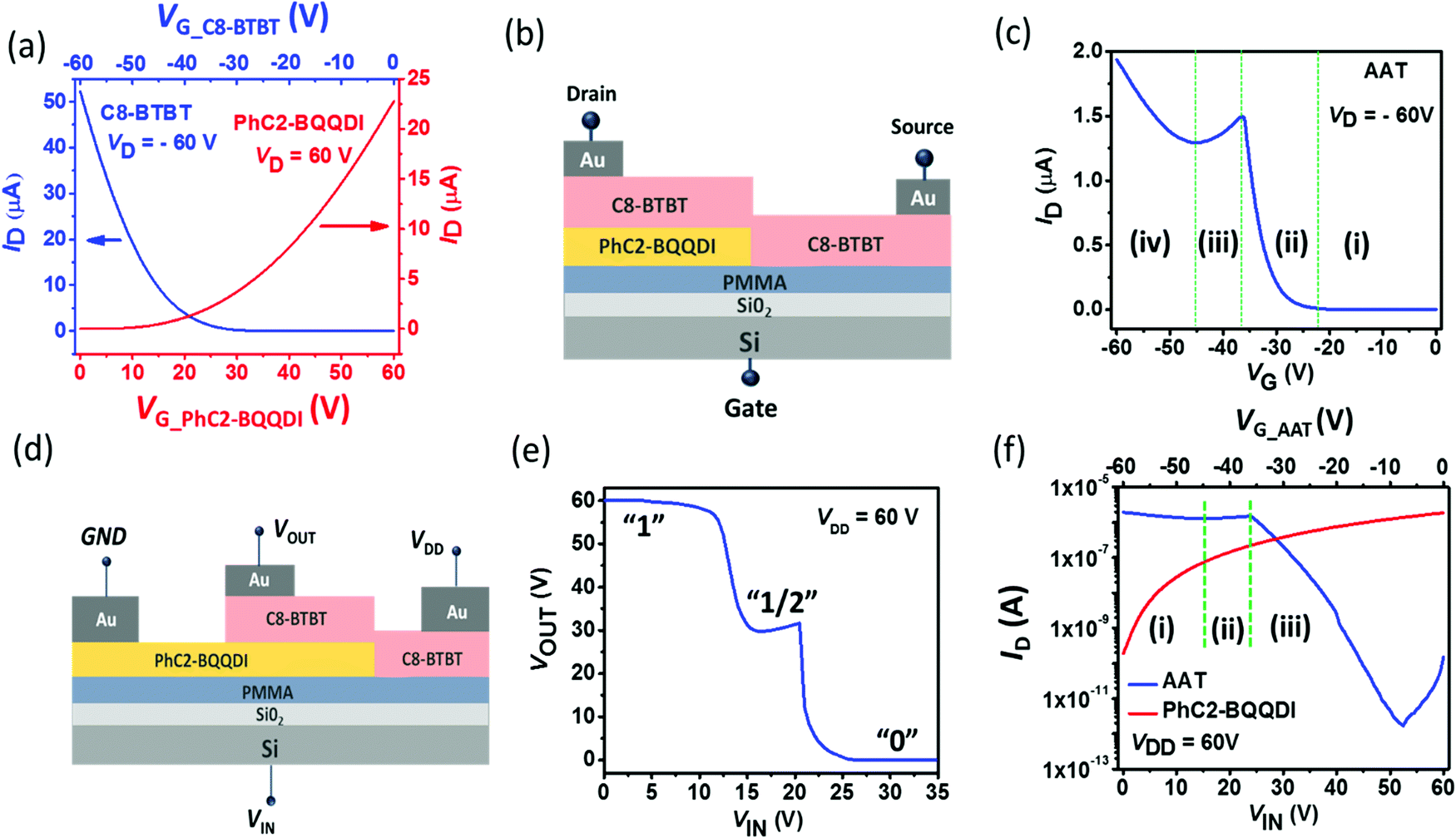 | ||
| Fig. 1 (a) Transfer characteristics (at VD = |60| V) of the PhC2-BQQDI (red line) and C8-BTBT (blue line) transistors. (b) Schematic illustration of the AAT. (c) Transfer curve of the AAT at VD = −60 V. (d) Schematic illustration of the ternary inverter consisting of the AAT and the PhC2-BQQDI transistor. (e) Voltage transfer characteristics of the ternary inverter at VDD = 60 V. (f) Transfer characteristics of the AAT and PhC2-BQQDI transistor measured at VDD = 60 V. | ||
Subsequently, AATs were prepared based on the performances of the two organic transistors. Fig. 1(b) shows a schematic illustration of the AATs. Here, both the source and drain electrodes are placed on the C8-BTBT layer, and a lateral heterojunction of the C8-BTBT and PhC2-BQQDI layers is formed between the two electrodes. As reported by Kim et al.,27 this transistor structure enhances the hole current in the p-type operation and is advantageous in yielding full-swing ternary inverter operation. Fig. 1(c) shows the transfer curve of the AAT in the p-type operation. The transfer characteristics can be divided into four distinct VG ranges. In range (i), the source to gate voltage (VSG) was insufficient to form the p-type channel. As a result, the devices remained in the off state. In this range, a minimum drain current (IOFF) of 1 pA was observed at VG = −7.5 V. In range (ii), ID started increasing with increasing VG because of the hole accumulation in the C8-BTBT channel. Namely, both C8-BTBT and PhC2-BQQDI channels became conductive. Due to the high charge carrier mobilities of these semiconducting layers, ID increased rapidly and attained a high peak value (Ipeak) of 1.5 μA at VG = Vpeak = −37 V. Then, in range (iii), ID started decreasing with increasing VG due to the depletion of the PhC2-BQQDI channel. ID fell from 1.5 μA to 1.2 μA at the end of this range (VG = −45 V), yielding the NDT range. Finally, in range (iv), the device showed a second current enhancement range, where ID started increasing again in the VG range above −45 V owing to the presence of the continuous C8-BTBT layer, which provided a conductive path that allowed the holes to reach the drain electrode. At the end of this range (VG = −60 V), the AATs exhibited the maximum drain current (ION) of 2 μA. Thus, the proposed AATs achieved a high on/off ratio (ION/IOFF) of 106 owing to the high charge carrier mobility of the constituent organic semiconductors.
The unique transfer characteristics of the AATs, including the NDT range and high on/off ratio, enabled us to obtain a complete VDD to ground voltage sweep in the ternary inverter circuit. The logic circuit was constructed by using a series connection of the AAT and an n-channel PhC2-BQQDI transistor as illustrated in Fig. 1(d). The supply voltage (VDD = 60 V) and input voltage (VIN) were applied to the drain electrode of the AAT and the common gate electrode, respectively. The source electrode of the PhC2-BQQDI transistor was grounded and the output voltage (VOUT) was monitored at the middle-shared electrode. Here it is important to note that the VOUT electrode is electrically connected to PhC2-BQQDI transistor through C8-BTBT layer and the layer doesn’t impede the underlying n-type operation of the PhC2-BQQDI transistor. The optical microscope image of the inverter is shown in Fig. S3 (ESI†). The ternary inverter exhibited three distinct logic states as shown in Fig. 1(e): logic 1 at VOUT = VDD = 60 V, logic 1/2 at VOUT = VDD/2 = 30 V and logic 0 at VOUT = ground. The inverter operation can be understood from the transfer characteristics of the constituent AAT and PhC2-BQQDI transistor as shown in Fig. 1(f). At a low VIN (range (i)), the ID of the AAT was much higher than that through the PhC2-BQQDI transistor which formed a conductive path between VDD and the output terminal and thereby yielded VOUT = VDD (logic 1). In the intermediate VIN (range (ii)), where the NDT was induced in the AAT, both transistors showed comparable ID values. As a consequence, VDD was divided into the two transistors, resulting in a middle logic state (logic 1/2). Importantly, the channel lengths of the AAT (100 μm) and PhC2-BQQDI transistor (300 μm) were optimized to achieve the ideal VOUT balance between the logic 1 and logic 1/2 states. This is because the VOUT levels of the inverter logic states depend on the resistance balance between the constituent transistors.41 In the high VIN (range (iii)), the PhC2-BQQDI transistor exhibited markedly higher ID values compared with that of the AAT. Therefore, a conducting path between the output terminal and ground was created to result in VOUT = ground logic 0. It should be noted that the complete VOUT sweep from VDD to the ground in the inverter was realized by the following two contributing factors. One is the observed current enhancement in the AAT at a high VG range (range (iv) in Fig. 1(c)), which originated from the continuous C8-BTBT channel. The enhanced ID assisted VOUT to attain VDD in the logic 1 operation. The other factor is the large difference in the ID values of the AAT and PhC2-BQQDI transistor. The difference of several orders of magnitude in the ID (ranges (i) and (iii) in Fig. 1(f)) helped VOUT to reach VDD in the logic 1 state and decrease to ground voltage in the logic 0 state, respectively. In most cases, the full VDD to ground sweep in ternary inverters has not been obtained because of the insufficient difference in the ID values of the constituent transistors.6,14,21 The use of transistor channels with high carrier mobilities provided an advantage in this regard. High carrier mobility of the semiconductors realized a high on/off ratio in each constituent transistor, resulting in a large difference in ID at low and high VIN range of the inverter operation. Thus, the synergic effect of device geometry and superior transport properties of the material combination enabled us to achieve a complete VDD to ground modulation in the ternary inverters along with the ideal VOUT ratio of 0.5 between logic 1/2 and logic 1.
However, the obtained VTC was still not suitable for the practical use of the ternary inverter because no SNM for the logic 1/2 state appeared as shown in Fig. S4 (ESI†). The poor SNM of the inverters mainly originated from the narrow width of the logic 1/2 state. Given an ideal ternary inverter, at VIN = VDD/2, VOUT should be equal to VDD/2.42,43 In contrast, in our devices, at VIN = 30 V, logic 0 state was obtained instead of logic 1/2 state. Namely, no cross section in the logic 1/2 state was observed in the inverter butterfly curve (Fig. S4, ESI†). Therefore, maximization of the logic 1/2 width was requisite to obtain the enough SNM in the logic 1/2 state.
To overcome the drawback, we adopted a strategy which is geometry optimization of the AATs. Since logic 1/2 width depends on the NDT range of the AATs, we optimized the ratio (RL) between the length of PhC2-BQQDI channel (LPhc2-BQQDI) and the length of C8-BTBT channel (LC8-BTBT) (i.e. RL = LPhc2-BQQDI: LC8-BTBT) to enhance the NDT range in the AATs. A schematic illustration of the AAT structure is shown in Fig. 2(a) to define the two parameters, LPhc2-BQQDI and LC8-BTBT. LPhc2-BQQDI indicates the length of PhC2-BQQDI channel from the lateral edge of the heterojunction to the drain electrode (D), whereas LC8-BTBT signifies the length of C8-BTBT channel from the lateral edge of the heterojunction to the source electrode (S). Fig. 2(b) and (c) show the optical microscope images with the different RL values and the transfer characteristics of the corresponding devices. In the transistor with RL = 1![[thin space (1/6-em)]](https://www.rsc.org/images/entities/char_2009.gif) :5, namely with the shortest LPhc2-BQQDI, no NDT range was observed. The AATs only showed a normal p-type transistor operation because the charge carriers flow only through the continuous C8-BTBT layer. Then, with varying RL from 1:5 to 1:2, NDT range appeared as guided by the red dashed line in Fig. 2(c) and the NDT range gradually increased from 0 V to 16 V. This is because the electrons and holes start flowing across the lateral heterojunction and the effect of electron depletion becomes more pronounced with the increasing LPhc2-BQQDI. Finally, at RL = 1:1, no further enhancement of NDT range was observed. Along with the variation in the NDT range, a shift in Vpeak was also observed towards positive VG from −36 V to −25 V when RL was varied from 1:3 to 1:2. Nevertheless, at RL = 1:1, Vpeak returned again towards a negative VG of −32 V. It is noted that Vpeak determines the transition input voltage from logic 1/2 to logic 0 in the ternary inverter. Besides, the NDT range coincides with the logic 1/2 width. From these points of view, RL = 1:2 emerged as the optimized AAT geometry to achieve a long logic 1/2 width (∼16 V) and a suitable transition voltage from logic 1/2 to logic 0 (VIN ∼ 35 V for Vpeak ∼ −25 V) in the ternary inverter.
:5, namely with the shortest LPhc2-BQQDI, no NDT range was observed. The AATs only showed a normal p-type transistor operation because the charge carriers flow only through the continuous C8-BTBT layer. Then, with varying RL from 1:5 to 1:2, NDT range appeared as guided by the red dashed line in Fig. 2(c) and the NDT range gradually increased from 0 V to 16 V. This is because the electrons and holes start flowing across the lateral heterojunction and the effect of electron depletion becomes more pronounced with the increasing LPhc2-BQQDI. Finally, at RL = 1:1, no further enhancement of NDT range was observed. Along with the variation in the NDT range, a shift in Vpeak was also observed towards positive VG from −36 V to −25 V when RL was varied from 1:3 to 1:2. Nevertheless, at RL = 1:1, Vpeak returned again towards a negative VG of −32 V. It is noted that Vpeak determines the transition input voltage from logic 1/2 to logic 0 in the ternary inverter. Besides, the NDT range coincides with the logic 1/2 width. From these points of view, RL = 1:2 emerged as the optimized AAT geometry to achieve a long logic 1/2 width (∼16 V) and a suitable transition voltage from logic 1/2 to logic 0 (VIN ∼ 35 V for Vpeak ∼ −25 V) in the ternary inverter.
 | ||
| Fig. 2 (a) Schematic illustration of the AAT demonstrating the channel lengths, LPhc2-BQQDI and LC8-BTBT. (b) Different geometries of the AATs. (c) Geometry dependent transfer characteristics (at VD = −60 V) of the AATs. (d) Vpeak and NDT ranges of the AATs as a function of PhC2-BQQDI to C8-BTBT channel length ratio (RL). (e) Butterfly curve of the ternary inverter at VDD = 60 V for RL = 1:2 with the estimated SNM. (f) Gain values of the inverter as a function of applied input voltage. | ||
Fig. 2(e) shows the butterfly curve of the ternary inverter with the optimized AAT geometry. In accordance with the transfer characteristics of the AAT, the inverter exhibited an improved VTC with logic 1 at VOUT = 60 V (0 V < VIN < 12.5 V), logic 1/2 at VOUT = 35 V (19 V < VIN < 36 V) and logic 0 at VOUT = ground (45 V < VIN < 60 V). The enhanced logic 1/2 width induced an SNM of 7.49 V in the ternary inverter, which was 35% of the ideal value ( VDD/4 = 21.21 V).33 The gain values obtained at VIN = 15 V (the transition input voltage from logic 1 to logic 1/2) and VIN = 40 V (the transition input voltage from logic 1/2 to logic 0) were 16 V/V and 18 V/V, respectively, as shown in Fig. 2(f). As described above, the geometry optimization achieved some improvement in the VTC of the ternary inverter. However, the obtained SNM still does not satisfy the requirements in the practical applications.
Finally, we utilized the contrasting optical responses of the C8-BTBT and PhC2-BQQDI semiconductors to further improve the SNM of the inverters. Fig. 3(a) and (b) show the impact of UV and visible light irradiation on the PhC2-BQQDI and C8-BTBT transistors, respectively. The visible light irradiation had two major impacts on the transfer characteristics of the PhC2-BQQDI transistor. One was drain current enhancement, which was induced by the generation of charge carriers. At VG = VD = 60 V, ID was increased from 22 μA in the dark to 27 μA under visible light irradiation (Fig. 3(a)). The other impact was a threshold voltage reduction of 2 V, which was caused by the accumulation of minority charge carriers in the channel region.44–46 Under light irradiation, a large number of excitons were generated in the PhC2-BQQDI layer due to its characteristic absorption in the visible light wavelength range (Fig. S5, ESI†). These excitons were then separated into electrons and holes under the applied electric field. After the separation, the majority carriers (electrons in PhC2-BQQDI) easily flowed towards the drain electrode whereas the minority carriers (holes in PhC2-BQQDI) remained at the interfaces as well as in the channel region due to their marginal mobility. The accumulated minority charge carriers reduced the potential barrier at the source/channel interface and then promoted charge injection from the source electrode, which led to the reduction in the threshold voltage. In contrast to the result with visible light, the PhC2-BQQDI transistor properties remained completely invariant under UV light irradiation. On the other hand, the C8-BTBT transistor exhibited photoresponsivity only under UV light irradiation (Fig. 3(b)) because of the characteristic absorption in the UV range (Fig. S5, ESI†). The Vth value of the devices decreased by 9 V together with an increase in the ID value from 52 μA in the dark to 88 μA under UV light irradiation at VG = VD = −60 V. In marked contrast to the PhC2-BQQDI transistor, the C8-BTBT transistor did not respond to visible light irradiation. This contrasting light induced variations in the PhC2-BQQDI and C8-BTBT layers resulted in an opposite shift in the inverter VTC under visible and UV light as shown in Fig. 3(c). The shift in the inverter output characteristics was also supported by the light induced shift in the transfer characteristics of the AATs as shown in Fig. S6 in the ESI.† Under visible light, the VTC was shifted towards a lower VIN due to the Vth shift in the PhC2-BQQDI layer. The suppression of ID in the AATs under visible light, which is caused by the recombination of holes with the photo-generated electrons, also triggered this shift as observed in Fig. S6 (ESI†). Due to this visible light influenced shift in the VTC, the width of logic 1 state and the driving VIN were reduced, i.e., the ternary logic states were obtained with a lower input voltage. On the other hand, the VOUT level of the logic 1/2 state was enhanced because of the generation of charge carriers in the PhC2-BQQDI layers, which altered the resistance ratio between the AAT and the PhC2-BQQDI transistor. These impacts upon visible light irradiation makes the VTC unbalanced. In contrast to the effect of visible light, the UV light irradiation induced a shift in the inverter VTC towards a higher VIN due to the Vth shift of the C8-BTBT layer. This shift, in turn, extended the width of the logic 1 state. The width of the logic 1/2 state also increased due to the enhancement of the NDT range in the AATs. These UV-light-triggered variations in the inverter characteristics are expected to improve the SNMs in the ternary inverters. Therefore, we investigated the influence of UV light intensities on the inverter characteristics to explore the light tunability in a more quantitative way for the further optimization of the SNMs.
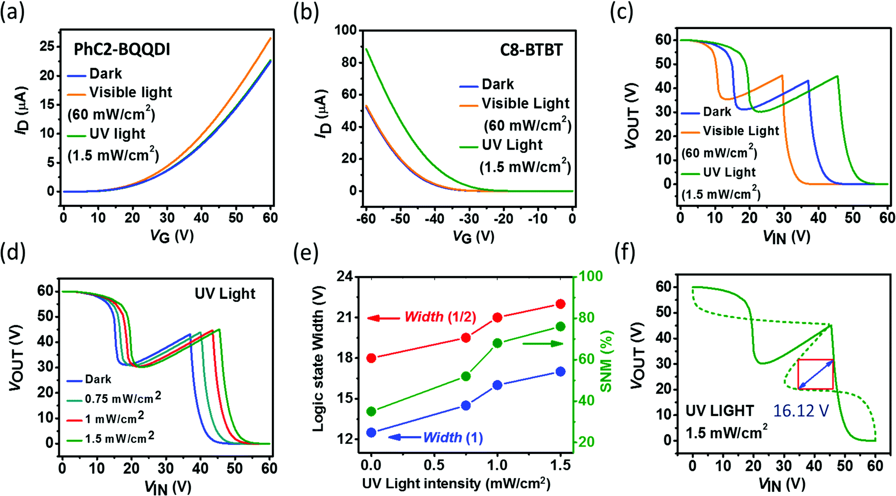 | ||
| Fig. 3 Transfer characteristics (at VD = |60| V) of the (a) PhC2-BQQDI and (b) C8-BTBT transistors, in the dark (blue lines), under visible light (orange lines) and under UV light irradiation (green lines). (c) Voltage transfer characteristics of the inverters in the dark (blue line), under visible light (orange line) and under UV light irradiation (green line). (d) Voltage transfer characteristics of the inverters under UV light inputs with various intensities. (e) Logic state widths and the values of SNM as a function of UV light intensity. (f) Voltage transfer characteristics of the inverter under UV light intensity of 1.5 mW cm−2 and the extracted value of SNM. | ||
Fig. 3(d) shows the VTC with different UV light intensities. The widths of logic 1 and logic 1/2 are denoted as width (1) and width (1/2), respectively, and are plotted as a function of the UV light intensity in Fig. 3(e). Width (1) (blue line in Fig. 3(e)) increased monotonically with the increase in the UV light intensity from 12.5 V in the dark condition to 17 V under a UV light intensity of 1.5 mW cm−2. Width (1/2) (red line in Fig. 3(e)) also exhibited a gradual enhancement from 17 V to 22 V. These UV light induced improvements in the logic state widths were reflected in the SNM of the ternary inverters. The SNM values increased from 7.5 V under dark condition to 16.1 V under the UV light intensity of 1.5 mW cm−2, which was 76% of the ideal value. The butterfly curve of the ternary inverter under the UV light intensity of 1.5 mW cm−2 is shown in Fig. 3(f). The butterfly curves under the UV light intensities of 0.75 mW cm−2 and 1 mW cm−2 are shown in Fig. S7 (ESI†). In this manner, the use of UV light was found to be an effective technique not only to fine-tune the logic state widths and but also to induce a high endurance against the electrical noises in the ternary inverters.
Meanwhile, it is worth mentioning that although the VTC of the inverters degraded under visible light in terms of SNM (Fig. S8, ESI†), the contrasting photo response of the inverters under visible and UV light makes them suitable candidates for their potential application as inverter-based UV and visible light detectors. The primary advantage of the inverter-based photodetectors is their superior ability to convert the optical signals into the voltage output signals. This feature has the potential to overcome the difficulty in the measurement of nano-ampere (nA) level current signals, which is a major problem in the conventional photocurrent-based photodetectors.47
Thus, the contrasting optical responses of C8-BTBT and PhC2-BQQDI semiconductors enable us to control the logic state properties improving the SNM of the inverters. Furthermore, this feature also opens up the possibility for the inverters to be used as photodetectors. In a similar manner, optically tunable MVL has been reported in α-6T/PTCDI-C8 and MoSe2/WSe2 systems.29,35 In α-6T/PTCDI-C8 system, the photoresponse of α-6T was superior to that of PTCDI-C8 under both UV and visible light irradiation, and this impeded effective light tunability. In addition, visible and UV light was found to degrade the VOUT level of logic 1 and logic 1/2 state, respectively.29 On the other hand, in MoSe2/WSe2 system, both MoSe2 and WSe2 responded under 638 nm light irradiation. As a result, the light irradiation was found to be useful to enhance the VOUT level of logic 1/2 state. However, no effective controllability in the logic state positions and widths were observed.35 The combination of C8-BTBT and PhC2-BQQDI provides an advantage in this regard. We can separately activate C8-BTBT or PhC2-BQQDI using a UV or visible light signal and precisely control the width, position and VOUT level of the inverter logic states. Furthermore, improvement in the noise immunity of the inverters were achievable through UV light signals, which reveals the merits of the proposed devices in opto-electronic logic applications.
3. Conclusion
In conclusion, we demonstrated an organic NDT transistor based on a heterojunction consisting of a new material combination, namely C8-BTBT for the p-type and PhC2-BQQDI for the n-type semiconductors, respectively. Due to the high carrier mobility of these materials, the proposed AATs were able to exhibit a high on/off ratio of 106. These AATs also enabled us to achieve a complete VOUT swing from VDD to ground and an ideal logic 1/2 to logic 1 VOUT ratio of 0.5 in the ternary inverters. Then, the AAT geometry was properly optimized to enhance the inverter logic 1/2 width. However, the obtained VTC were still not suitable for the practical applications of the inverters due to the poor SNM. Therefore, in order to improve the SNM, we demonstrated an efficient technique of UV light irradiation on the ternary inverters, which enabled an optical control on the inverter VTC and yielded a high SNM of 76%. The contrasting photoresponsivity of C8-BTBT/PhC2-BQQDI material combination played the most critical role in this regard. This work, thus, represents progress towards the development of light tunable, high performance organic MVLs for future opto-electronic logic applications.4. Experimental section
The transistors and inverters were fabricated on highly doped Si wafers with a 200 nm-thick SiO2 layer, which worked as a bottom gate electrode and a dielectric layer, respectively. Prior to the device fabrication, the substrates were properly cleaned by ultra-sonication with acetone and isopropanol. They were then rinsed in deionized water and dried in a nitrogen gas flow. Then, a thin layer (∼10 nm) of poly(methyl methacrylate) (PMMA) was spin-coated on top of the SiO2 surface to passivate the surface defects and to facilitate the transport of the charge carriers at the dielectric–semiconductor interface.26,48 Thereafter, organic semiconductors, PhC2-BQQDI (∼16 nm) and C8-BTBT (∼19 nm), were thermally evaporated on the PMMA surface as n-type and p-type channels, respectively, at a background pressure of 10−7 Pa using corresponding shadow masks. These two semiconductors were partially overlapped to form the heterojunction, which played a major role to give rise to the NDT characteristics. Fixed deposition rates of 0.8 Å min−1 and 1.0 Å min−1 were maintained for the PhC2-BQQDI and C8-BTBT layers, respectively. Finally, gold (Au) source and drain electrodes were deposited on the organic semiconductors by thermal evaporation using another shadow mask to complete the AAT structure. The channel length and width of the AATs were 100 μm and 350 μm, respectively. The ternary inverters were produced by connecting the AAT with an n-channel PhC2-BQQDI transistor in series.All electrical measurements were performed in a vacuum (∼10−1 Pa) using an Agilent B1500A semiconductor parameter analyser. The photoresponse of the devices was monitored using a xenon lamp as the light source. Reflecting mirrors were used to extract the UV and visible light, which had wavelength ranges of 300–385 nm and 385–800 nm, respectively.
Conflicts of interest
There are no conflicts to declare.Acknowledgements
This research was supported by the World Premier International Center (WPI) for Materials Nanoarchitectonics (MANA) of the National Institute for Materials Science (NIMS), Tsukuba, Japan, and JSPS KAKENHI grant number 19H00866.References
- H. J. Park, C. J. Park, J. Y. Kim, M. S. Kim, J. Kim and J. Joo, ACS Appl. Mater. Interfaces, 2018, 10, 32556 CrossRef CAS PubMed.
- K. Kobashi, R. Hayakawa, T. Chikyow and Y. Wakayama, Adv. Electron. Mater., 2017, 3, 1700106 CrossRef.
- K. Kobashi, R. Hayakawa, T. Chikyow and Y. Wakayama, ACS Appl. Mater. Interfaces, 2018, 10, 2762 CrossRef CAS PubMed.
- C. Lee, J. Choi, H. Park, C. Lee, C.-H. Kim, H. Yoo and S. G. Im, Small, 2021, 17, 2103365 CrossRef CAS PubMed.
- X. Jiang, M. Zhang, L. Liu, X. Shi, Y. Yang, K. Zhang, H. Zhu, L. Chen, X. Liu, Q. Sun and D. W. Zhang, Nanophotonics, 2020, 9, 2487 CAS.
- Y. Hassan, P. K. Srivastava, B. Singh, M. S. Abbas, F. Ali, W. J. Yoo and C. Lee, ACS Appl. Mater. Interfaces, 2020, 12, 14119 CrossRef CAS PubMed.
- K. H. Kim, H. Y. Park, J. Shim, G. Shin, M. Andreev, J. Koo, G. Yoo, K. Jung, K. Heo, Y. Lee and H. Y. Yu, Nanoscale Horiz., 2020, 5, 654 RSC.
- J. H. Lim, J. Shim, B. S. Kang, G. Shin, H. Kim, M. Andreev, K. S. Jung, K. H. Kim, J. W. Choi, Y. Lee and J. H. Park, Adv. Funct. Mater., 2019, 29, 1905540 CrossRef CAS.
- Y. Wang, W. X. Zhou, L. Huang, C. Xia, L. M. Tang, H. X. Deng, Y. Li, K. Q. Chen, J. Li and Z. Wei, 2D Mater., 2017, 4, 025097 CrossRef.
- Y. Wakayama and R. Hayakawa, Adv. Funct. Mater., 2020, 30, 1903724 CrossRef CAS.
- J. Shim, S.-H. Jo, M. Kim, Y. J. Song, J. Kim and J.-H. Park, ACS Nano, 2017, 11, 6319 CrossRef CAS PubMed.
- J. B. Kim, J. Li, Y. Choi, D. Whang, E. Hwang and J. H. Cho, ACS Appl. Mater. Interfaces, 2018, 10, 12897 CrossRef CAS PubMed.
- W. Lv, X. Fu, X. Luo, W. Lv, J. Cai, B. Zhang, Z. Wei, Z. Liu and Z. Zeng, Adv. Electron. Mater., 2018, 5, 1800416 CrossRef.
- A. Nourbakhsh, A. Zubair, M. S. Dresselhaus and T. Palacios, Nano Lett., 2016, 16, 1359 CrossRef CAS PubMed.
- S. L. Hurst, IEEE Trans. Comput., 1984, 12, 1160 Search PubMed.
- S. L. Hurst, Opt. Eng., 1986, 25, 250144 CrossRef.
- B. Fresch, M. V. Klymenko, R. D. Levine and F. Remacle, Computational Matter, 2018, p. 295 Search PubMed.
- K. R. Kim, J. W. Jeong, Y. E. Choi, W. S. Kim and J. Chang, J. Semicond. Eng., 2020, 1, 57 Search PubMed.
- V. Levashenko, I. Lukyanchuk, E. Zaitseva, M. Kvassay, J. Rabcan and P. Rusnak, IEEE TCAD, 2020, 39, 4854 Search PubMed.
- J. Shim, S. Oh, D.-H. Kang, S.-H. Jo, M. H. Ali, W.-Y. Choi, K. Heo, J. Jeon, S. Lee, M. Kim, Y. J. Song and J.-H. Park, Nat. Commun., 2016, 7, 1 Search PubMed.
- M. Huang, S. Li, Z. Zhang, X. Xiong, X. Li and Y. Wu, Nat. Nanotechnol., 2017, 12, 1148 CrossRef CAS PubMed.
- Z. Wang, X. He, X. X. Zhang and H. N. Alshareef, Adv. Mater., 2016, 28, 9133 CrossRef CAS PubMed.
- D. Jariwala, V. K. Sangwan, C. C. Wu, P. L. Prabhumirashi, M. L. Geier, T. J. Marks, L. J. Lauhon and M. C. Hersam, Proc. Natl. Acad. Sci. U. S. A., 2013, 110, 18076 CrossRef CAS PubMed.
- J. Dong, F. Liu, F. Wang, J. Wang, M. Li, Y. Wen, L. Wang, G. Wang, J. He and C. Jiang, Nanoscale, 2017, 9, 7519 RSC.
- C. J. Park, H. J. Park, J. Y. Kim, S. H. Lee, Y. Lee, J. Kim and J. Joo, Semicond. Sci. Technol., 2020, 35, 065020 CrossRef CAS.
- K. Kobashi, R. Hayakawa, T. Chikyow and Y. Wakayama, Nano Lett., 2018, 18, 4355 CrossRef CAS PubMed.
- H. Yoo, S. On, S. B. Lee, K. Cho and J. J. Kim, Adv. Mater., 2019, 31, 1808265 CrossRef PubMed.
- J. Liu, J. Liu, J. Zhang, C. Li, Q. Cui, F. Teng, H. Li and L. Jiang, J. Mater. Chem. C, 2020, 8, 4303 RSC.
- D. Panigrahi, R. Hayakawa, K. Fuchii, Y. Yamada and Y. Wakayama, Adv. Electron. Mater., 2020, 7, 2000940 CrossRef.
- D. Wu, W. Li, A. Rai, X. Wu, H. C. P. Movva, M. N. Yogeesh, Z. Chu, S. K. Banerjee, D. Akinwande and K. Lai, Nano Lett., 2019, 19, 1976 CrossRef CAS PubMed.
- S. B. Jo, J. Kang and J. H. Cho, Adv. Sci., 2021, 8, 2004216 CrossRef CAS PubMed.
- H. Yoo and C.-H. Kim, J. Mater. Chem. C, 2021, 9, 4092 RSC.
- E. Wu, Y. Xie, Q. Liu, X. Hu, J. Liu, D. Zhang and C. Zhou, ACS Nano, 2019, 13, 5430 CrossRef CAS PubMed.
- M. E. Beck and M. C. Hersam, ACS Nano, 2020, 14, 6498 CrossRef CAS PubMed.
- S. Hong, H. J. Park, H. W. Cho, J. Park, S. Kim and H. Yoo, 2020, Tunable Intermediate-logic Ternary Circuits based on MoSe2-WSe2 Heterojunction, 2020 DOI:10.21203/rs.3.rs-108643/v1.
- N. R. Glavin, C. Muratore and M. Snure, Open Mater. Sci. J., 2021, 1, itaa002 Search PubMed.
- J. Pu, K. Funahashi, C.-H. Chen, M.-Y. Li, L.-J. Li and T. Takenobu, Adv. Mater., 2016, 28, 4111 CrossRef CAS PubMed.
- H. Sirringhaus, Adv. Mater., 2014, 26, 1319 CrossRef CAS PubMed.
- D. Panigrahi, R. Hayakawa, K. Honma, K. Kanai and Y. Wakayama, Appl. Phys. Express, 2021, 14, 081004 CrossRef CAS.
- M. Uno, N. Isahaya, B.-S. Cha, M. Omori, A. Yamamura, H. Matsui, M. Kudo, Y. Tanaka, Y. Kanaoka, M. Ito and J. Takeya, Adv. Electron. Mater., 2017, 3, 1600410 CrossRef.
- C. H. Kim, R. Hayakawa and Y. Wakayama, Adv. Electron. Mater., 2020, 6, 1901200 CrossRef CAS.
- S. Shin, E. Jang, J. W. Jeong, B. G. Park and K. R. Kim, IEEE Trans. Electron Devices, 2015, 62, 2396 Search PubMed.
- M. Takbiri, R. F. Mirzaee and K. Navi, Circuits, Syst. Signal Process., 2019, 38, 4280 CrossRef.
- N. Marjanović, T. B. Singh, G. Dennler, S. Günes, H. Neugebauer, N. S. Sariciftci, R. Schwodiauer and S. Bauer, Org. Electron., 2006, 7, 188 CrossRef.
- D. Panigrahi, S. Kumar and A. Dhar, Polymer, 2017, 130, 79 CrossRef CAS.
- R. Liguori, W. C. Sheets, A. Facchetti and A. Rubino, Org. Electron., 2016, 28, 147 CrossRef CAS.
- F. Liu, Y. Zhang, J. Wang, Y. Chen, L. Wang, G. Wang, J. Dong and C. Jiang, Nanotechnology, 2020, 32, 015203 CrossRef PubMed.
- S. G. J. Mathijssen, M. Kemerink, A. Sharma, M. Cölle, P. A. Bobbert, R. A. J. Janssen and D. M. de Leeuw, Adv. Mater., 2008, 20, 975 CrossRef CAS.
Footnote |
| † Electronic supplementary information (ESI) available. See DOI: 10.1039/d1tc05858d |
| This journal is © The Royal Society of Chemistry 2022 |