
Plasmonic PHOLEDs: increasing OLED stability
Michael S.
Weaver
 *,
Michael A.
Fusella
,
Renata
Saramak
,
Rezlind
Bushati
,
Haridas
Mundoor
,
Vinod M.
Menon
,
Nicholas J.
Thompson
and
Julia J.
Brown
*,
Michael A.
Fusella
,
Renata
Saramak
,
Rezlind
Bushati
,
Haridas
Mundoor
,
Vinod M.
Menon
,
Nicholas J.
Thompson
and
Julia J.
Brown
Universal Display Corporation, 375 Phillips Blvd., Ewing, NJ 08618, USA. E-mail: mikeweaver@oled.com
First published on 23rd February 2022
Abstract
This paper introduces a novel organic light emitting device that intentionally couples phosphorescent emitters to the surface plasmon mode of the metal cathode. A ∼2× decay rate enhancement is observed, resulting in a ∼50% increase in constant current density device stability. A nanoparticle-based plasmon out-coupling scheme efficiently converts the energy in the cathode to photons in free space and results in a doubling of the operational device stability at fixed initial brightness. These gains are achieved independent of materials design.
1. Introduction
Organic light emitting devices (OLEDs) are incorporated into billions of displays generating >$38 billion in revenues annually. The demonstration of an efficient planar heterojunction device1 in 1986 started OLEDs on a path to commercial products. Further efficiency improvements were realized by utilizing a guest host emissive layer system.2 Emission from this early OLED work was from fluorescent materials where the internal quantum efficiency (IQE) is limited to approximately 25% as triplet excitons cannot emit radiatively in these materials. In contrast, in a phosphorescent OLED (PHOLED) system, all the singlet excited state excitons may be converted into the triplet excited state through inter-system crossing (S1 to T1) via the presence of a heavy metal atom.3 Although phosphorescence increased the internal quantum efficiency to 100%, today's commercial OLEDs are planar, which limits the external quantum efficiency (EQE) of the device due to a mismatch in refractive index between the organic stack and air.4 Typical OLEDs convert ∼25%, and at best ∼50%,5 of the charges injected into photons in free space with no external outcoupling. A method for increasing the EQE beyond 50% without adding light extracting elements6,7 or engineering particular material properties8 would provide a roadmap for new commercial opportunities.In this paper we demonstrate a new type of OLED which utilizes the surface plasmon mode of thin metallic films to give rise to broadband decay rate enhancements.9 Using the surface plasmon mode as a fast energy sink increases the device stability by decreasing the buildup of excitons with the energy recovered as light using nanoparticle antennae (NPA) based plasmon outcoupling scheme. This novel OLED architecture breaks the conventional OLED operation paradigm and increases stability and efficiency compared to conventional devices. The new device architecture is applied to a green phosphorescent emitter fac-tris(2-phenylpyridine) Iridium(III) (Ir(ppy)3), hosted by 2,4-diphenyl-6-bis((12-phenylindolo)[2,3-a]carbazole-11-yl)-1,3,5-triazine (DIC-TRZ) where the new ‘plasmonic PHOLED’ device exceeds the efficiency and stability of a conventional OLED reference device.
2. Experimental
Patterned indium tin oxide (ITO) coated glass substrates with a sheet resistance of 16–19 Ω/□ are cleaned with organic solvents, treated with oxygen plasma and UV-ozone. Organic materials and metals are thermally evaporated in vacuum with base pressure <10−2 Pa. The device active area is 2 mm2 and device structures are depicted in Fig. 1. The plasmon non-NPA device is identical in structure to the plasmon NPA device, with the omission of the last layer of Ag nanocubes. HIL is the hole injection layer, HTL is the hole transport layer, EBL is the electron blocking layer, EML is the emission layer (containing Ir(ppy)3 doped at 12% by volume in DIC-TRZ), HBL is the hole blocking layer, ETL is the electron transporting layer, EIL is the electron injection layer, Gap is the spacer layer between the cathode and Ag nanocubes. The chemical structures for each layer are shown in Fig. 2. In the thin EML PHOLED, aluminum was used as an adhesion layer for Ag to improve the quality of the Ag cathode film, as has previously been used in OLEDs.10,11 A distinct adhesion layer was incorporated into the plasmonic PHOLED devices, which still utilize Ag cathodes. Aluminum was used as the cathode in the conventional PHOLED. | ||
| Fig. 1 Device structures used in this paper. Note that structures are not drawn to scale. | ||
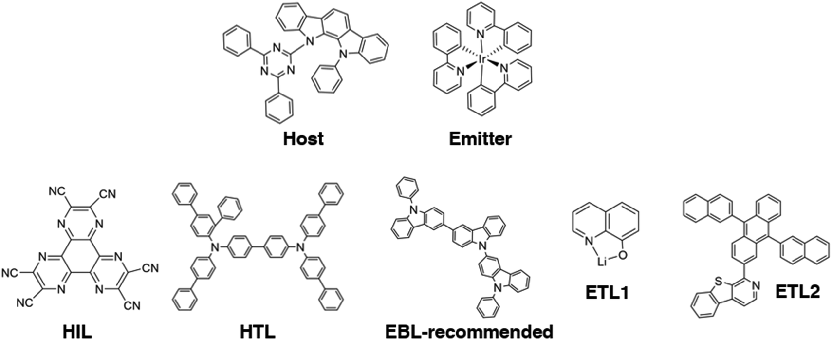 | ||
| Fig. 2 Organic materials used in the OLEDs of Fig. 1. The HTL material is also used as the GAP material. The EBL used in the work is proprietary, but the material labeled ‘EBL recommended’ is a drop-in replacement. The ETL is composed of ETL1 doped at 40% by volume with ETL2. ETL1 (lithium quinolate) was also used as the EIL in the devices of Fig. 1. | ||
75 nm silver nanocubes (commercially sourced from nanoComposix) are concentrated in ethanol solution via centrifugation (5200 × g for 10 min) to 5 mg mL−1 and spin cast (3000 rpm, 40 s) on top of the Gap layer of the OLED. The device is subsequently dried in vacuum for 15 minutes to remove any remaining solvent. A glass/epoxy cap and desiccant are then applied in a nitrogen glovebox to encapsulate the structures.
3. Results
In a conventional OLED the energy coupled to the surface plasmon mode typically cannot be recovered.4 Here we demonstrate that the plasmonic mode of an OLED9 can be used to increase stability and efficiency. Fig. 1 schematically depicts the plasmonic PHOLED device architecture which has several distinct features versus a conventional OLED. Firstly, the EML is thinned to only 5 nm and is located 16 nm from the top silver cathode. A conventional OLED typically has a 30–40 nm EML located >30 nm from the cathode. In the plasmonic PHOLED this results in strong coupling between the emitters in the EML and the surface plasmon mode of the silver contact. This strong coupling produces a large decay rate enhancement which decreases the emitter excited state duration. Secondly, the cathode is thinner at only 34 nm thick and has an additional organic layer (gap layer) plus, in the case of the plasmon NPA device, randomly distributed Ag nanoparticles. The cathode, gap layer, and Ag nanoparticles together form the outcoupling NPA. The gap layer is used to space the nanocubes from the cathode at a distance that maximizes plasmon-to-photon conversion efficiency. Light is then emitted to free space out the top of the device as the NPA converts energy within the surface plasmon mode of the Ag cathode to photons. Lastly, the ITO anode means that the device can simultaneously emit out the top (TE) and bottom (BE) of the device enabling the outcoupling efficiency to be quantified. For all four device architectures, the inset to Fig. 3 shows the electroluminescence (EL) spectra are characteristic of Ir(ppy)3.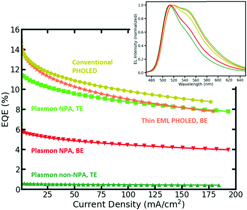 | ||
| Fig. 3 EQE vs. current density for the plasmonic PHOLED and the conventional OLED reference devices. For the plasmonic PHOLED, the TE (green squares) and BE (red downward triangles) are plotted as well as the TE EQE (dark green upward triangles) without the nanocube based outcoupling scheme. Inset are the corresponding normalized electroluminescent spectra. Note that the emission is narrowed for the plasmon non-NPA TE emission as the device is in essence a microcavity. | ||
The plasmonic PHOLED modifies the operation of a conventional OLED in the following way: injected charges are transported through the device under an applied electric field, these charges are converted to excitons, the excitons decay non-radiatively via coupling to the surface plasmon mode. The NPA-based outcoupling scheme then releases to free space the energy within the surface plasmon mode. These various steps are shown in the plot of EQE vs. current density of Fig. 3. The EQE of a conventional PHOLED (yellow circles) which has EML thickness of 40 nm, a 35 nm thick ETL, and an opaque cathode leading to bottom emission is plotted. An additional thin EML PHOLED reference was plotted (orange stars) with a thin 5 nm EML which matches the EML thickness of the plasmonic PHOLED. This EML is spaced 65 nm from an opaque Ag cathode leading to minimal coupling of the emitters in the EML to the cathode plasmon mode. The TE EQE of the plasmon NPA device is plotted in green squares. The TE light is from the surface plasmon mode of the top Ag contact. The TE EQE of same device without the addition of the Ag nanoparticles (plasmon non-NPA) is also plotted (dark green upward triangles). Lastly, the BE EQE of the plasmon NPA device is plotted (red downward triangles). This is the energy that is not coupled into the surface plasmon mode of the top Ag cathode.
Several key points are derived from Fig. 3. Firstly, at low current density, reducing the thickness of the EML does not impact efficiency as the two conventional OLED references align. Secondly, the inclusion of the Ag nanoparticles increases the amount of TE light from the plasmonic PHOLED. As the Ag cathode and nanoparticles are on the top of the PHOLED, we infer that this EQE results from energy coupled to the top Ag cathode surface plasmon mode. The TE EQE of the plasmon non-NPA device reduces the EQE below 1% at 10 mA cm−2 which shows there is little residual emission transmitted through the Ag cathode and no outcoupling of the energy stored within the plasmonic mode of the Ag contact without the nanoparticle based outcoupling scheme. Finally, the summation of BE and TE light from the plasmon NPA device exceeds that of the conventional OLED references demonstrating that a net gain in energy which can be outcoupled to air is possible using the plasmonic PHOLED versus a conventional PHOLED.
The inset in Fig. 3 shows differences in the electroluminescence (EL) spectra of the various devices. Compared to the BE spectrum of the conventional PHOLED, we see that the TE of the plasmon non-NPA is narrower due to the cavity effect. In contrast, the TE of the plasmon NPA device is broader than the plasmon non-NPA TE as a result of the scattering from the randomly arranged nanoparticles dominating the TE and also due to the resonance of the NPA being slightly red shifted with respect to the intrinsic emitter spectrum. Moreover, the plasmon NPA BE spectrum demonstrates a reduction in the intensity of the shoulder at 550 nm, partly due to cavity effects and because the bottom emission has little contribution from the red-shifted NPA-outcoupled light that dominates TE. The thin EML PHOLED BE spectrum differs from the conventional PHOLED again due to cavity effects, as the distance from the EML to the cathode differs between the two structures.
Fig. 4 shows the normalized luminance versus time, for the plasmonic PHOLED (green squares), the conventional OLED (yellow circles), and the thin EML conventional OLED reference (orange stars) when aged at a fixed accelerated current density of 80 mA cm−2. The thin EML PHOLED has the shortest lifetime due to the increased concentration of charges and excitons present in the thin EML. The plasmonic PHOLED luminance decays at the slowest rate. This is attributed to a reduced excited state duration due to the excited state coupling to the surface plasmon mode of the Ag cathode. Table 1 shows the 1931 Commission Internationale de l’éclairage (CIE) colour coordinates and the EL transient decay times for each device. The plasmonic PHOLED reduces the electroluminescence transient. With a decreased excited state duration, the steady-state concentration of excitons in the emissive layer is reduced leading to an increased stability despite the thin 5 nm EML thickness. We note that the LT95 for the plasmon NPA device is the same regardless of whether BE or TE is monitored in the accelerated aging experiment, as it is still the aging rate of the emitter molecules in the EML that sets the stability no matter which side is monitored.
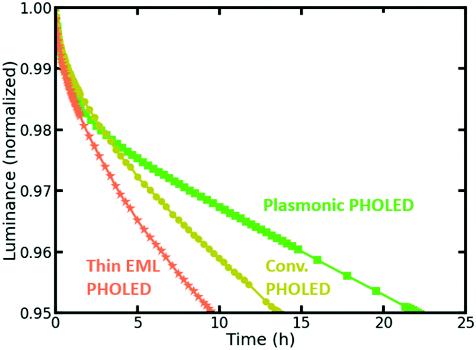 | ||
| Fig. 4 Lifetime curves of the plasmonic PHOLED and reference thin and conventional EML devices aged at 80 mA cm−2. | ||
| Device architecture | 1931 CIE (x, y) | EL transient decay (τ1, ns) | EQE 10 mA cm−2 (%) | LT95 80 mA cm−2 (h) | LT95 10![[thin space (1/6-em)]](https://www.rsc.org/images/entities/char_2009.gif) 000 cd m−2 (h) 000 cd m−2 (h) |
Initial brightness 80 mA cm−2 (cd m−2) |
|---|---|---|---|---|---|---|
| Conventional reference OLED standard EML | (0.320, 0.623) | 521 | 13 | 15 | 76 | 29177 |
| Conventional reference OLED thin EML | (0.331, 0.617) | 404 | 13 | 10 | 78 | 26992 |
| Plasmonic PHOLED TE | (0.337, 0.613) | 271 | 11 | 22 | 148 | 25113 |
| Plasmonic PHOLED BE + TE | — | — | 17 | 22 | 334 | — |
We also investigated the impact of the density and size of nanocubes used in conjunction with the plasmonic PHOLED. There is a strong dependence of the top emission (TE) EQE on the density of the cubes on top of the device. We find that the density of cubes on top of the device increases as the concentration of cube solution spin-cast on the device increases. Fig. 5 is a plot of TE EQE vs. current density for a plasmon NPA device where the cubes were spin-cast on the device from either 3 mg ml−1 or 5 mg ml−1 solutions vs. no cubes as well as AFM images of the two cube densities. We observed that the TE EQE saturates and concentrations above 6 mg ml−1 did not further increase the amount of energy outcoupled from the device.
 | ||
| Fig. 5 (a) Top emission EQE vs. current density of the plasmonic PHOLED device coated with three different nanocube concentrations. The TE EQE scales with increasing nanocube density, which is proportional to the nanocube concentration in solution. Atomic force micrograph (AFM) images of spin-coated (b) 5 mg ml−1 and (c) 3 mg ml−1 nanocube films. The nanocube fill fraction for the 5 mg ml−1 and 3 mg ml−1 films are 15% and 9%, respectively. | ||
Regarding cube size, we find that as the nanocubes become larger, the resonance of the NPA red-shifts and lessens the overlap of the NPA with the emission of Ir(ppy)3, which, in turn, lowers the TE EQE (see Fig. 6). Going to a smaller cube also results in lower TE EQE as the scattering efficiency of the outcoupling scheme is less as the localized surface plasmon mode of the cube is more absorbing.
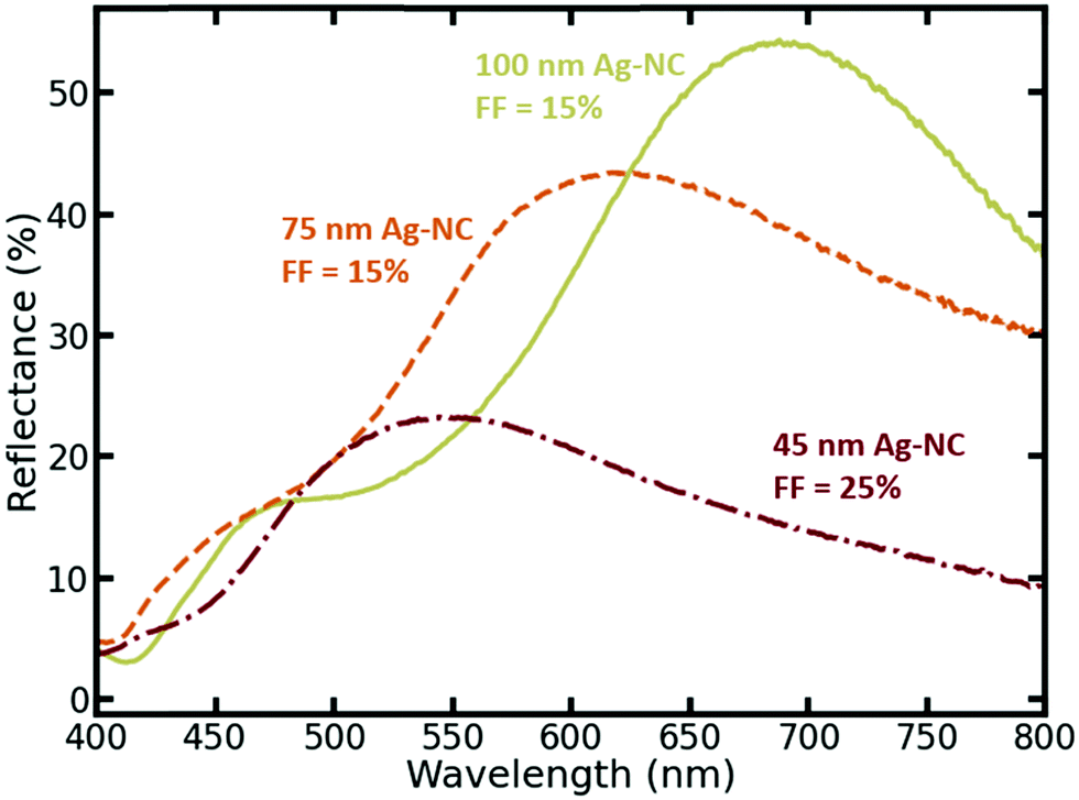 | ||
| Fig. 6 Diffuse reflectance plots of the NPA structure as measured via UV-vis spectroscopy for 100 nm, 75 nm, and 45 nm Ag nanocubes. As the Ag nanocube size increases the NPA resonance red-shifts and increases in intensity. The film fill fraction (FF) as measured by AFM is denoted for reference. | ||
4. Discussion
There are large gains in the plasmonic PHOLED device stability at fixed luminance because the plasmonic PHOLED stability is increased at a fixed driving current density and the TE EQE of the device is nearly equal to that of the BE EQE reference PHOLEDs. The plasmonic PHOLED luminance adjusted operational lifetime compared to the conventional devices at an accelerated aging condition of 80 mA cm−2 is shown in Table 1. The TE plasmonic PHOLED device loses 5% of its initial 10000 cd m−2 brightness in 148 hours compared to reference devices of 78 hours. Considering the light emitted from both sides of the plasmonic PHOLED device (BE + TE), its operational stability increases to 334 hours. This is four times greater operational stability versus the reference device. In addition, the increase in luminance adjusted stability is not linearly dependent on the excited state transient which only decreased by a factor of two. This suggests even larger stability enhancements can be readily achieved if the excited state transient can be further reduced or a greater outcoupling enhancement can be achieved from the plasmon modes. While having quantitative access to both plasmon-outcoupled (TE) and residual (BE) emission is important for scientific understanding, commercial implementations of this architecture would likely only utilize single-sided plasmon outcoupled light. In this case, the BE light could be reflected out the top via a reflective bottom contact, or, ideally, no residual (BE) light would be produced due to unity plasmon in-coupling efficiency.
5. Conclusions
The TE EQE, BE EQE, transient EL, and radiative rate of the emitter in the EML were used to understand the efficiency limitations of a plasmonic PHOLED. We determined that 22% of the excitons coupled into the surface plasmon mode of the Ag are converted to photons out the top of the device. Therefore the outcoupling efficiency of this plasmonic PHOLED is less than that of conventional planar OLEDs which can approach 40% EQE.5 In the plasmonic PHOLED the outcoupling efficiency is determined by the properties of the nanoparticle outcoupling scheme rather than the OLED material properties. This means that plasmonic PHOLEDs enable independent modification of the outcoupling and OLED materials to increase the device efficiency to >40% EQE. In addition to longer device lifetime and increased efficiency our choice of randomly arranged Ag nanocubes as the outcoupling mechanism achieves a Lambertian emission profile. A conventional TE OLED uses a micro-cavity to realize top emission resulting in a non-Lambertian emission profile. No color shift is observed for light at large angles in our plasmonic PHOLED architecture. With further refinements in outcoupling structure, plasmonic PHOLEDs will enable low color shift OLED displays with even higher efficiency and stability compared to today's commercial OLEDs.Conflicts of interest
M.S.W., M.A.F., R.S., H.M., N.J.T. and J.J.B. are employed at UDC and have personal financial interests via UDC stock ownership and numerous granted and pending patent applications on phosphorescent emitters and OLEDs. Work by R.B. and V.M.M. on this project was completed as part of their consultancy for UDC; they declare no additional competing interests.Acknowledgements
The research staff of Universal Display Corporation are acknowledged for their technical assistance and discussions.References
- C. W. Tang and S. A. VanSlyke, Appl. Phys. Lett., 1987, 51(12), 913 CrossRef CAS.
- C. W. Tang, S. A. VanSlyke and C. H. Chen, J. Appl. Phys., 1989, 65(9), 3610 CrossRef CAS.
- M. A. Baldo, D. F. O’Brien, Y. You, A. Shoustikov, S. Sibley, M. E. Thompson and S. R. Forrest, Nature, 1998, 395(6698), 151 CrossRef CAS.
- W. Brütting, J. Frischeisen, T. D. Schmidt, B. J. Scholz and C. Mayr, Phys. Status Solidi A, 2013, 210(1), 44 CrossRef.
- K.-H. Kim, S. Lee, C.-K. Moon, S.-Y. Kim, Y.-S. Park, J.-H. Lee, J. W. Lee, J. Huh, Y. You and J.-J. Kim, Nat. Commun., 2014, 5, 4769 CrossRef CAS PubMed.
- S. Möller and S. R. Forrest, J. Appl. Phys., 2002, 91(5), 3324 CrossRef.
- M.-K. Wei and I.-L. Su, Opt. Express, 2004, 12(23), 5777 CrossRef PubMed.
- H. Shin, J.-H. Lee, C.-H. Moon, J.-S. Huh, B. Sim and J.-J. Kim, Adv. Mater., 2016, 28(24), 4920 CrossRef CAS PubMed.
- M. A. Fusella, R. Saramak, R. Bushati, V. M. Menon, M. S. Weaver, N. J. Thompson and J. J. Brown, Nature, 2020, 585(7825), 379 CrossRef CAS PubMed.
- L. S. Hung, C. W. Tang, M. G. Mason, P. Raychaudhuri and J. Madathil, Appl. Phys. Lett., 2001, 78, 544 CrossRef CAS.
- J. H. Im, K.-T. Kang, S. H. Lee, J. Y. Hwang, H. Kang and K. H. Cho, Org. Electron., 2016, 33, 116 CrossRef CAS.
| This journal is © The Royal Society of Chemistry 2022 |