
 Open Access Article
 This Open Access Article is licensed under a Creative Commons Attribution-Non Commercial 3.0 Unported Licence
Impedance spectroscopy for perovskite solar cells: characterisation, analysis, and diagnosis
Elizabeth
von Hauff†
 *ab and
Dino
Klotz†
*cd
*ab and
Dino
Klotz†
*cd
aFraunhofer Institute for Organic Electronics, Electron Beam and Plasma Technology (FEP), Dresden, Germany. E-mail: Elizabeth.von.Hauff@fep.fraunhofer.de
bFaculty of Electrical and Computer Engineering, Technical University of Dresden, Dresden, Germany
cInternational Institute for Carbon-Neutral Energy Research (I2CNER), Kyushu University, Fukuoka, Japan. E-mail: dino.klotz@i2cner.kyushu-u.ac.jp
dDepartment of Materials Science and Engineering (DMSE), Massachusetts Institute of Technology (MIT), Cambridge, USA
First published on 8th December 2021
Abstract
Impedance spectroscopy (IS) has great potential to become a standard technique for the characterisation, analysis, and diagnosis of perovskite solar cells (PSC). However, the interpretation of IS data from PSC is still challenging due to the large number of dynamic processes which are not yet fully understood. Here we provide a general framework for IS analysis on PSC. We begin by reviewing the timescales reported for electrical and electrochemical dynamics, many of which are too fast or too slow to monitor with IS, and yet they have a significant impact on the impedance spectrum of PSC. To account for this, we review guidelines for obtaining high quality impedance spectra, including suitable measurement settings as well as the relevant device physics at different solar cell operating points. Based on this, we propose a universal equivalent circuit model (ECM) that exploits the fact that impedance spectra from perovskite solar cells ubiquitously demonstrate high and low frequency signatures that are separated by several orders of magnitude. We show that the high frequency signatures are consistent with fast electronic processes, while the low frequency signatures are consistent with electrochemical processes such as ion drift and diffusion and electrochemical reactions. This allows us to propose a simple, robust, and adaptable ECM that can be used to parameterise relevant material parameters as well as monitor loss mechanisms for all PSC materials and architectures.
Introduction
Perovskite solar cells (PSC) have demonstrated remarkable increases in efficiency,1 and more recently also notable improvements in stability2 over the last decade. In the current stage of development, operando characterisation and diagnosis are becoming increasingly important to engineer the transition towards commercialisation. Measurement protocols for current (density)–voltage curves (JV curves) that yield benchmark data for efficiency, open circuit voltage (VOC), fill factor (FF), short circuit current density (JSC) and the hysteresis index (HI) have been established in the literature, and are a straightforward way to characterise fully contacted devices under relevant operating conditions. However, JV measurements alone do not offer insight into the nature of the different dynamic processes that determine and limit solar cell performance.Impedance spectroscopy (IS) is a versatile characterisation technique to monitor electrical and electrochemical processes operando, as well as profile the electronic structure in electrochemical and solid-state devices. In an IS measurement, the response of the sample to a small-signal, sinusoidal electrical stimulus is monitored as a function of the frequency. The electrical energy of the excitation signal is dissipated and/or stored by the device, depending on the characteristic dynamics being probed. The dynamics, or relaxation processes, can be differentiated if they show a unique relaxation time (or time constant), i.e. the measure for how long it takes for the device to equilibrate after excitation. The information is extracted and quantified from the spectrum using equivalent circuit models (ECM), and the values of the corresponding parameters offer insights into the underlying physical nature of these different processes. IS can be easily performed in complement to standard electrical characterisation, and has proven to be very useful for elucidating different performance-relevant processes and parameters in energy conversion and storage devices.3
In electrochemical cells, IS has been widely used to model charge transfer and chemical reactions at the electrode–electrolyte interface, as these dynamic processes are generally accessible within the IS measurement window.4,5 Analogous techniques such as Capacitance-frequency (Cf) and deep-level transient spectroscopy (DLTS), which can be summarised as defect spectroscopy techniques, probe electronic structure instead of dynamics, in particular doping and trap profiles of device junctions and interfaces.6–8 The difference between IS and defect spectroscopy is the mode of operation in which the device is characterised.9 For IS, the device is measured at a relevant operational DC offset bias in order to quantify electrical or electrochemical dynamics that determine and impact performance. In contrast, for defect spectroscopy, the change in the capacitance of the depleted semiconductor as a function of temperature, voltage, and/or frequency is monitored to determine the energetic distribution of traps. Therefore, the device must be operated in depletion mode for the measurement, i.e. changes in capacitance are only due to the changes in the density of bound charge in the depleted semiconductor. This has proven challenging in emerging PV, as the band diagram and therefore processes determine carrier transport are often not well enough understood to ensure that the depletion approximation is satisfied for the measurement. In this case, additional capacitive signatures due to mobile charge10,11 result in artefacts in the frequency spectra and errors in the analysis.
Historically in photovoltaic (PV) research, defect spectroscopy has been more commonly applied than electrochemical IS combined with ECM. This is because the electronic dynamics in silicon and thin film PV are generally too fast to monitor with IS, and defect spectroscopy reveals more useful information related to trap and doping profiles. In the field of emerging PV, however, IS has been gaining increasing attention. Dye sensitised solar cells (DSSC), as electrochemical devices, are well-suited for IS measurements.12–14 Organic photovoltaics (OPV) are solid-state devices with comparatively slow transport processes, where both IS15,16 and defect spectroscopy10,17,18 have been applied to study transport, electronic structure, and interfacial phenomena.
Perovskite solar cells (PSC) were first reported in 2009![[thin space (1/6-em)]](https://www.rsc.org/images/entities/char_2009.gif) 19 and in the wake of rapidly increasing efficiencies, many researchers from other PV communities, including DSSC and OPV, joined the perovskite community. As a result, IS studies on PSC were motivated by earlier insights gained from DSSC and OPV devices. This was only partly successful because in PSC, both ionic and electronic carriers may contribute to the IS signatures, and a wide range of electrical and electrochemical processes take place at the device interfaces. Further, device stability and reproducibility have been rather poor in the past, making it difficult to obtain reliable IS data. Finally, variations in PSC compositions and architectures, combined with different IS measurement protocols, have made it challenging to compare different IS spectra in the literature and extract general features. As a result, there are currently no universally accepted protocols for performing IS on PSC, nor are there universal models for interpreting IS results.
19 and in the wake of rapidly increasing efficiencies, many researchers from other PV communities, including DSSC and OPV, joined the perovskite community. As a result, IS studies on PSC were motivated by earlier insights gained from DSSC and OPV devices. This was only partly successful because in PSC, both ionic and electronic carriers may contribute to the IS signatures, and a wide range of electrical and electrochemical processes take place at the device interfaces. Further, device stability and reproducibility have been rather poor in the past, making it difficult to obtain reliable IS data. Finally, variations in PSC compositions and architectures, combined with different IS measurement protocols, have made it challenging to compare different IS spectra in the literature and extract general features. As a result, there are currently no universally accepted protocols for performing IS on PSC, nor are there universal models for interpreting IS results.
We, by no means, intend to disregard the extensive, careful, and insightful work that has been done on PSC. We refer the interested reader to examples of this previous work, for example a comprehensive introduction is provided in ref. 20, model approaches are discussed based on the thickness of the absorber layer, illumination intensity, and applied voltage in ref. 21; in ref. 22 this approach is extended to take into account influences of layer thicknesses and contacts, in ref. 23, the dynamic behaviour of PSC is studied in combination with other complementary techniques such as open circuit photovoltage decay (OCVD) and intensity-modulated photovoltage spectroscopy (IMVS). Additional practical guidelines for consistent IS measurements are provided in ref. 24
A quick survey through the literature reveals an apparent variation between the impedance spectra measured on PSC, including differences in the magnitude of the impedance values, as well as the appearance of features in the Nyquist plots that are difficult to physically interpret, such as negative hooks or loops.22,23,25–27 However, closer inspection reveals that there is a commonality of nearly all impedance spectra from PSC, namely the general appearance of high frequency (HF) and low frequency (LF) features which are separated in the frequency spectrum by several orders of magnitude, as shown in Fig. 1.
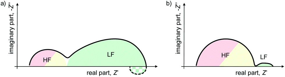 | ||
| Fig. 1 Example schematics of impedance spectra for PSC with HF contribution smaller/larger than LF contribution, with/without negative hook. While sizes and ratios of the diameters of these features can differ, most spectra reported in the literature show shapes that can be seen as variations of the two examples shown here. | ||
The nature of these HF and LF signatures have not yet been unequivocally assigned in the literature, although recent studies have demonstrated that the HF signature is consistent with electrical transport while the LF signature is consistent with electrochemical dynamics.28,29 In a later section, we explain how the HF signature can be attributed to electronic dynamics in the PSC, while LF signatures are classic signatures of electrochemical dynamics.
Our aim is to provide guidelines for applying IS to study the performance and stability of PSC, as well as to apply IS as a diagnostic tool to identify mechanisms leading to performance loss. We begin by reviewing dynamic processes in PSC and their timescales. This serves as the basis for interpreting and assigning the HF and LF signatures in the IS from PSC. We then review the basics of IS along with rules of good practice for obtaining reliable IS data. Next, we correlate the IS response at different operating points with the JV characteristics from state-of-the-art PSC. Finally, we combine these concepts to suggest a basic, empirical and universal approach to circuit modelling for PSC. This approach facilitates the comparison of IS performed on different PSC architectures, and thereby provides the basis for IS as an operando diagnosis tool for performance characterisation and monitoring, and improved physical insight into failure modes in PSC.
Timescales of dynamics in perovskite solar cells
An understanding of the timescales of dynamics occurring in the operational PSC during measurement is an important starting point for developing reliable IS measurement protocols and analyses. The challenge, specifically for IS on PSC, is that many of these processes occur on timescales outside the frequency range of the IS measurement (which is generally from microseconds to seconds), and yet, have a direct impact on the electrical response. These dynamics may still manifest in the IS spectrum as either a resistive or capacitive signature, but not as an independent relaxation process. Fast dynamics include electronic processes at short (picoseconds to microseconds) timescales, slow dynamics include (electro-)chemical processes on long (seconds to hours) timescales.30,31 These electrochemical processes will inevitably be determined by fabrication parameters, such as perovskite composition and the nature of the contact materials, and therefore the nature of these dynamics, e.g. timescale and reversibility, will vary.
Fig. 2 illustrates the different electronic, ionic, and (electro-) chemical dynamics in PSC and how these compare to the IS measurement window (shaded in dark blue). The relaxation time, τ, of each process is indicated on the upper scale bar, while the corresponding characteristic frequency f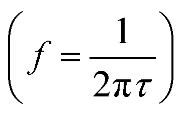 is indicated on the lower scale bar. The frequency ranges for the high frequency (HF) semicircles and low frequency (LF) signatures that are commonly observed in IS on PSC are also indicated.
 | ||
| Fig. 2 Timescales of dynamics in PSC. The top scale bar indicates the relaxation time τ of each process. The bottom scale bar indicates the corresponding frequency. The maximum measurement frequency possible in IS measurements without high-frequency compensation bridges is between 1–10 MHz. For the reliable characterisation of dynamics, the measurement frequency should be about an order of magnitude higher than the characteristic frequency. This limits characterisation at the high frequency end of the spectrum. At the lower end, the characterisation of slow processes is limited by more practical aspects such as measurement time, signal-to-noise, and device stability. | ||
Electronic processes in PSC (HF)
Electronic processes in PSC, such as carrier generation and cooling, radiative recombination (bimolecular recombination), transport, and trapping, are reported to occur on ns–ps timescales30,32 in studies that apply optical spectroscopy on perovskite layers and uncontacted (partial) devices under conditions corresponding to standard 1.5 AM illumination. As the samples were not electrically contacted for these studies, these measurement conditions correspond to open circuit voltage (VOC) conditions, where no current flows and all photogenerated carriers ideally recombine radiatively.Applying an external voltage to the solar cell results in the flow of current. Electrical transport of carriers to the electrodes can, in principle, be monitored with IS if the mobility is low and/or the carrier lifetime is long enough. However, in PSC the effective carrier lifetime is reported in the order of ns.33,34 As a result, carrier transport is too fast to monitor as a dynamic process with IS.
Trap-assisted, or Shockley–Read–Hall (monomolecular), recombination is a non-ideal recombination process that occurs when photocarriers recombine via defect states either at device interfaces (surface recombination) or in the perovskite, e.g. at grain boundaries.35 Trap-assisted recombination in PSC is reported to occur on timescales ranging between microseconds and 10s of microseconds.32,33,36,37 In other words, non-radiative recombination dynamics in PSC border on the threshold of the maximum frequency in the IS measurement window (MHz). It should be noted that non-radiative recombination dynamics (particularly at device interfaces) depend on processing, device architecture, and operating voltage, and therefore timescales may vary.32,38
We note two important points here. Firstly, that there is good agreement between the timescales for electronic processes reported in the literature. Secondly, all of the electronic dynamics in PSC are too fast to monitor as dynamic processes with IS, with the exception perhaps of slower non-radiative recombination losses. However, recent studies that combined experimental electrical measurements with modelling concluded that electrical characterisation techniques (including IS) cannot directly access the dynamics of electrical transport - including recombination - but instead interrogate secondary effects.39,40 Slower ionic transport or ionic migration occurring under illumination and/or applied bias results in a change in the electrostatic environment in the PSC,41 and this in turn results in slow changes in the electrical transport and recombination dynamics. In this scenario, the HF and LF signatures are interdependent. For example, carrier recombination in PSC was reported to display temperature-activation resembling the Meyer–Neldel (MN) rule,42 which is not characteristic for electrical recombination dynamics, but instead, is consistent with the MN behaviour reported for ion migration in PSC.31,41,43 For the analysis of IS, we will later see (cf.Fig. 7) that the geometric capacitance makes it essentially impossible to discern different dynamics within the HF signature. Therefore, more sophisticated analyses from the area of mixed conductors and solid-state electrochemistry could be very useful to elucidate electrical transport properties by exploiting the reciprocal nature of ionic and electrical transport in PSC.44
Electrochemical processes in PSC (LF)
Lower frequency (LF) signatures in IS on PSC are consistent with slow electrochemical dynamics, such as chemical reactions and ion migration. These processes are non-ideal photovoltaic processes. In other words, in contrast to ideal electrical processes such as electrical charge transport and recombination,45 electrochemical processes are not well described in terms of basic solar cell physics, and there are no generalised equations availabe for these processes in the context of PV. Therefore, identification of these LF signatures and the corresponding physical assignment requires a dedicated and systematic approach that, in the best case, includes corroboration with other experiment techniques as well as with simulation. This step is important since the electrochemical processes represent losses in the photovoltaic conversion process, as the incoming solar energy is converted into chemical processes rather than into electrical power.The frequency gap between the HF and LF signatures in IS
The HF and LF signatures in the IS of PSC have been discussed extensively in the literature, and many reports can be found describing the expected and observed HF and LF behaviour, respectively.23,39,40,46 However, we want to draw the attention to the ubiquitous frequency gap between HF and LF contributions. Neither theoretical studies nor reported experimental IS measurements on PSC predict or observe any process or characteristic impedance signature between 100 Hz (upper frequency bound of the LF signature) and 10 kHz (lower frequency bound of the HF signature). This is an important consideration for the interpretation and analysis of IS on PSC, and we will utilise this particularity in the ECM section to significantly simplify as well as to generalise our proposed ECM for PSC.Impedance Spectroscopy basics for PSC
Impedance Spectroscopy basics
To perform an IS measurement, a small-signal, sinusoidal electrical input signal (VAC) is superimposed on the applied DC voltage (VDC)| V(ωt) = VDC + VAC(ωt) = VDC + V0sin(ωt) | (1) |
| I(ωt) = IDC + IAC(ωt) = IDC + I0sin(ωt + φ) | (2) |
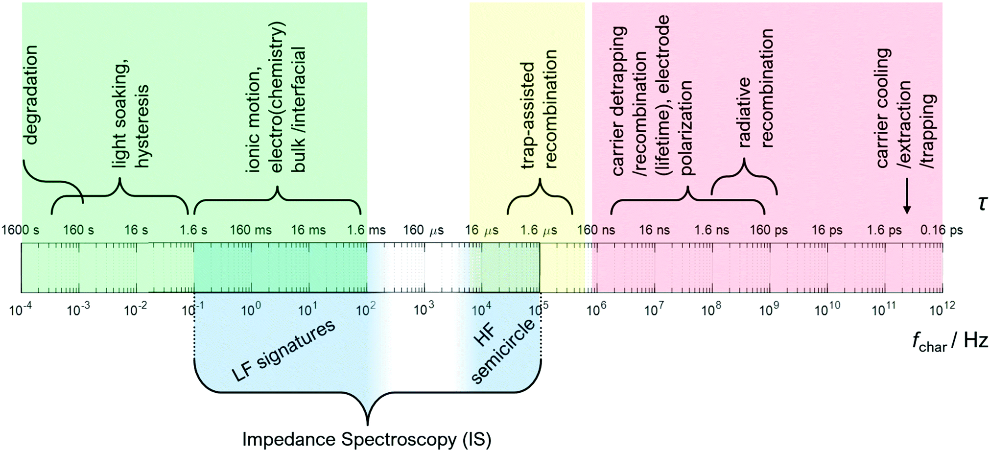
The amplitude V0 is chosen to maximise the signal-to-noise ratio while ensuring a linear current response, φ represents the difference in phase angle between the input voltage VAC and output current IAC in the frequency domain. Fig. 3a depicts the input voltage V0sin(ωt) and output current I0sin(ωt + φ) in the time domain, where Δt indicates the time delay between the voltage and current signals.
 | ||
| Fig. 3 (a) Time domain representation of the current and voltage signals (IAC and VAC) during an impedance measurement for one frequency with both signals harmonically oscillating at different amplitudes (^), and with a time delay (Δt) between VAC and IAC. (b) Schematic of a Nyquist plot with one complex impedance value Z(ω). (c) Circuit representation of a fundamental relaxation process with a finite resistance and a finite capacitance. (d) Nyquist plot of the impedance response over the full frequency range of an RC circuit. | ||
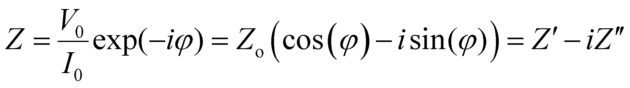
The impedance Z is a transfer function, i.e. a linear function that relates the input VAC to the output IACvia:
 | (3) |
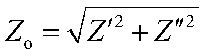 ) and phase angle (φ) for each value of frequency ω. Fig. 3b shows the projection of Z(ω) in the complex plane, where the real part of Z (Z′ or RE{Z}) is the resistance to current flow, or simply the resistance. The imaginary part of Z (Z′′ or IM{Z}) is the reactance, i.e. the resistance to changes in current flow. Generally, the relative contributions of Z′ and Z′′ to the total impedance vary with frequency. Equivalent circuit modelling (ECM) (see section ECM) relies on the assumption that the full impedance spectrum can be modelled with a combination of ideal circuit elements, such as resistors (R, φ = 0°), capacitors (C, φ = −90°), and/or inductors (L, φ = +90°), such that the frequency-dependence of Z can be parameterised.
Relaxation processes in the impedance spectrum
With IS, we are probing dynamics in the device. Provided the timescales of the dynamics are within the IS measurement window (Fig. 2), these dynamics manifest as relaxation processes in the impedance spectrum. Relaxation processes in IS can be expressed in terms of the characteristic resistance (R) and capacitance (C), correlated to the dissipation (φ = 0°) and storage (φ = 90°) of electrical energy of the excitation signal, respectively. Therefore, ideal relaxation processes are modelled with a resistor–capacitor (RC) circuit (Fig. 3c). The characteristic time constant τ of the RC circuit| τ = RC | (4) |
However, measurements on real samples rarely yield spectra with ideal relaxation processes.47 Specifically, measurements on semiconductor devices and electrochemical systems contain a combination of resistive and reactive signatures, resulting from material polarisation, electrical and ionic transport, interfacial charge transfer, chemical reactions, double layer formation, and/or charge recombination.3,9,48,49 These relaxation processes are often dispersive, meaning that there may be a distribution of time constants associated with a single dynamic process, for example, charge transfer at an inhomogeneous electrode surface.3 Further, relaxation processes may overlap in the Nyquist plot, making them either indistinguishable or causing them to appear as distorted.50 Here, ECM can help to identify and parameterise the individual contributions to the spectrum, which is why modelling is an essential step in impedance analysis.
Resistors and capacitors in impedance spectroscopy
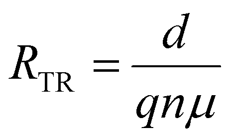
Relaxation processes inherently consist of the dissipation (resistance) and storage (capacitance or inductance) of electrical energy. To facilitate a physical interpretation of an ECM, it should be possible to express and quantify the individual R and C elements in terms of material parameters.The definition of the resistance R is not always precise in electrochemistry and photo-electrochemistry. While it is custom to use the area-specific quantity for current (A), i.e. the current density (A cm−2), often no distinction is made between the resistance (Ω) and the area-specific resistance (Ω cm2). In PSC literature, the term “area-specific resistance” is not commonly used so it may not be clear which quantity is being used. Therefore, we explicitly state that all resistances discussed here are area-specific (Ω cm2) unless otherwise stated. Analogously, we only consider the area specific capacitance (F cm−2). In the literature it is common to report current density to facilitate comparison between solar cell parameters in the literature. Analogously, using area-specific resistance and capacitance values facilitates comparison of the IS data.
To compare the theoretical values introduced here with (absolute) measurement data, the area-specific resistances introduced here have to be divided by the cell area, whereas the area-specific capacitances have to multiplied by the cell area.
 | (5) |
 | (6) |
 | (7) |
In addition to resistance due to bulk transport, resistive signatures may also manifest in the IS spectrum due to charge transfer and recombination.
 | (8) |
However, generally the resistive and capacitive signatures must be extracted from the impedance spectrum using an ECM.
Here we consider ideal capacitors to describe the underlying physics related to transport in solar cells. However, for equivalent circuit modelling of IS data from real samples, ideal capacitors often have to be substituted by constant phase elements to account for dispersion, i.e. variations in the timescale of a relaxation process due to sample inhomogeneity.
 | (9) |
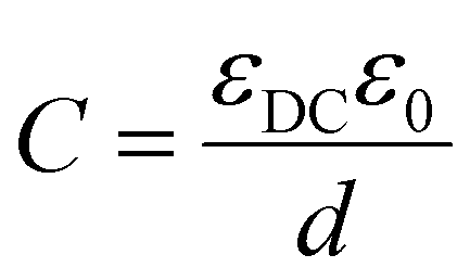
Geometric capacitances arise due to the polarisation of bulk materials, as well as interfaces. Therefore, the total geometric capacitance may comprise several individual capacitive contributions. Capacitances in series contribute to total capacitance CTOTAL reciprocally, i.e.
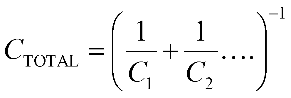
This means that the smallest capacitance dominates the total capacitance that is measured. This is the case when considering the PSC, in which the total geometric capacitance of the device is determined by the capacitance of the perovskite bulk in series with the capacitances at the contact interfaces. In this case, the bulk PSC is the lowest (as the film thickness of the bulk is generally orders of magnitude larger than that of the transport layers), and dominates.
For standard PSC with a thickness of the perovskite absorber of 500 nm and a dielectric constant of 10 to 20,22,57 the area-specific geometrical capacity of a PSC is 18 nF cm−2 to 35 nF cm−2.
 | (10) |
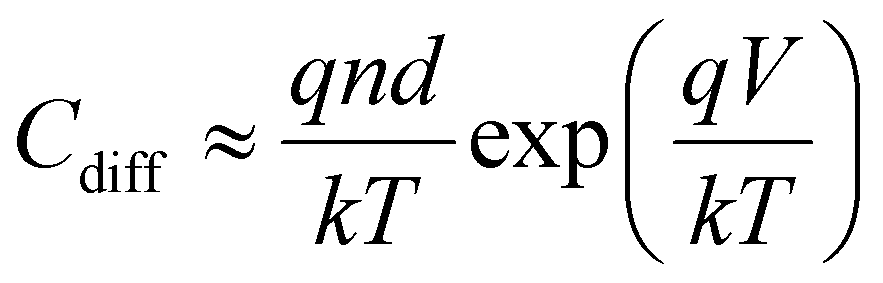
The diffusion capacitance Cdiff arises in forward-biased diodes due to the accumulation of minority carriers at the boundary of the depletion region. It depends on the voltage, which in turn determines the depletion region width as well as the density of minority carriers, and has the general form (normalised by the area)
 | (11) |
The diffusion capacitance is in parallel to drift transport in the solar cell.
The chemical capacitance Cμ arises in systems with a low density of charge, so that the excitation voltage used to perform the IS measurement causes a shift in the chemical potential (Fermi level) of the semiconductor due, e.g. the injection of charge at the contacts
 | (12) |
We summarise this section by noting that with exception of the transport resistance and the geometric capacitance, defining the resistive and capacitive elements in terms of more fundamental material and device parameters requires an understanding of the electronic band diagram, carrier dynamics, and, specifically in the case of PSC, also possible electrochemical dynamics. Identifying the physical nature of resistive and capacitive signatures is not always possible. Therefore, we note here that in the case that either the resistance or capacitance associated with a relaxation process is not easily physically interpreted, it is possible to fully describe the impedance response of a relaxation process with the timescale τ combined with either the R or C element. This approach, for example, resolves a major issue with negative loops, because one does not have to physically rationalise the emergence of negative capacity.59 However, as we will discuss in the later section ECM, in the case of PSC, the geometric capacitance makes it nearly impossible to identify and distinguish electronic dynamics. Therefore, we will present a strategy for the modelling of PSC that primarily focusses on distinguishing electronic and electrochemical dynamics, as well as understanding the reciprocity between electronic and electrochemical transport. Specifically, we argue that IS presents an opportunity to identify electrochemical dynamics, and monitor how these impact the electrostatic band diagram and carrier dynamics in PSC.
Lastly, we note that inductive signatures are frequently reported in IS studies on solar cells, including PSC.22,59,60 Inductive signatures can arise due to real physical effects, such as long (unshielded) cables.61 However, they may also arise due to capacitive signatures that lead the VAC excitation, instead of lagging behind it, resulting in a negative capacitance or inductance. In the literature, this has been attributed to trapping and surface recombination.60 We later discuss potential origins for negative capacitances in PSC related to ion migration.
Impedance measurements and analysis on perovskite solar cells
In this section we discuss good practice for IS measurement protocols for PSC. While PSC architectures vary in the literature, generally benchmark efficiencies for optimised devices are around 20%, with VOC and JSC values in the range of 1.0–1.2 V and 20–25 mA cm−2, respectively. That means that the area-specific electrical properties of these cells are comparable, resulting in resistive and capacitive signatures in IS of the same order of magnitude. This is a feature that has not been appreciated in the community to its full extent, and we believe that the quantitative comparison of IS features between optimised PSC has the potential to serve as basis for more refined diagnosis and comparison than JV curves.The solar cell JV curve is relatively simple to interpret in terms of the most relevant figures of merit (VOC, JSC, FF, MPP, efficiency, as well as stability and hysteresis). However, just as for other (photo-)electrochemical devices, the solar cell JV curve provides the sum of losses for all the cumulative processes that occur simultaneously. Those can only be deconvoluted if the underlying physics are known. More quantitative analysis of the JV curve using drift-diffusion simulations can provide additional information about the electrical properties, such as carrier conductivity and mobility, and recombination losses. However, these rely on detailed knowledge of these processes in order to perform accurate modelling. Further analysis of the temperature and light intensity dependence of the VOC can reveal insight into non-ideal losses that fundamentally limit solar cell efficiency. But even then, the JV curve of real solar cells is impacted by multiple, simultaneously occurring dynamic processes that cannot easily be extracted or distinguished using DC electrical measurements. In this regard, IS enables a separation of these dynamics in the frequency range, where the timescales of distinct relaxation processes emerge at characteristic frequencies in the spectrum. Therefore, impedance spectra taken at specific operating points along the JV contain information about dynamics that impact performance. Examining characteristic IS resistive and capacitive parameters and monitoring their values as a function of different fabrication protocols, for example for the geometric capacitance, offers direct access to values that can be quantitatively compared to parameters from the literature, and be used to identify signatures of faulty samples. Where applicable, standard values for characteristic IS resistor and capacitor parameters are summarised in section ECM (cf.Table 1) below. As a rule of thumb, if the obtained values are off by more than 50% it is a clear indication that something went wrong with the measurement, with the device, or with both.
| Element | Value | Description |
|---|---|---|
| R 0 | ∼10 Ω (absolute) | Series resistance from the current collectors |
| R t+r | ∼10–100 Ω cm2 | Charge carrier transport (drift/diffusion) and recombination resistance |
| C geo | ∼18–35 nF cm−2 | Geometrical capacity |
| R 1 | >0 | Related to scenario 1 (optional) |
| C 1 | >0 | Related to scenario 1 (optional) |
| R 2 | >0 | Related to scenario 2 (optional) |
| C 2 | >0 | Related to scenario 2 (optional) |
| R 3 | <0 | Related to scenario 3 (optional) |
| C 3 | <0 | Related to scenario 3 (optional) |
| R 4 | <0 | Related to scenario 4 (optional) |
| C 4 | <0 | Related to scenario 4 (optional) |
Fig. 4 shows the JV curve, power density versus voltage curve and the DC resistance calculated from the slope of the (smoothed) JV curve, taken from ref. 62, where also experimental details can be found. The corresponding PSC has a JSC of about 24 mA cm−2, a VOC of 1.11 V and an FF of 71%, which are typical values for a well-performing PSC under 100 mW cm−2 solar irradiation. The efficiency of about 20% is directly visible from the peak in the power density curve at MPP (20 mW cm−2 at 100 mW cm−2 irradiation). The DC resistance, i.e. the impedance for ω → 0, can be estimated from the slope of the JV curve and is shown in Fig. 4c. It provides an estimate of the magnitude of the impedance at very low frequencies. This example demonstrates that the expected values for the impedance vary by about three orders of magnitude over the full JV curve, depending on the operating voltage.
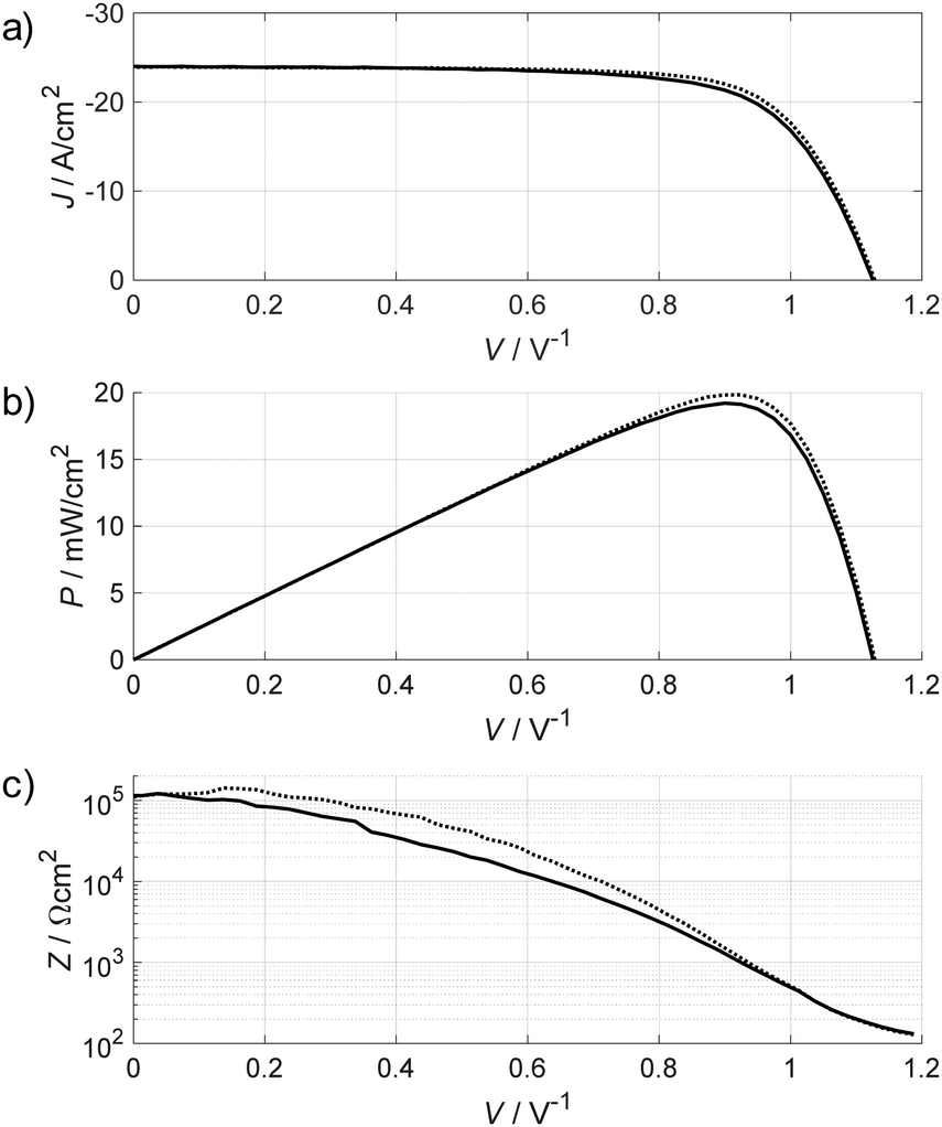 | ||
| Fig. 4 Example of (a) JV curve forward scan (0 V → VOC, dotted line) and backward scan (VOC → 0 V, full line) measured with a scan rate of 200 mV s−1; (b) power density calculated from the respective JV curves demonstrating the efficiency of ∼20% (20 mW cm−2 under standard 100 mW cm−2 illumination); (c) slope of the JV curve (calculated from raw JV data with a smoothing filter. The slope is equivalent to the expected ZDC = Z(ω → 0). It should be considered that the measurement of the JV curve is also a dynamic measurement and might not reflect the exact ZDC as a matter of principle. | ||
Next, we will discuss the expected, ideal impedance response from PSC at VOC, JSC, and MPP. Establishing a unified measurement protocol and guidelines for PSC at these operating points, complete with the expected resistive and capacitive response, enables the comparison of results from the literature, the possibility to join efforts to understand PSC behaviour in detail and, last but not least, to provide guidelines for newcomers to IS and/or PSC.
Operating points
Ensuring that IS measurements are performed at well-defined solar cell operating points is a necessary prerequisite for a useful comparison between IS data extracted from different PSC. The actual numeric values for VOC, JSC, and MPP may differ between devices, which means that the exact values chosen for the DC offset for the IS measurement should always be corroborated with JV measurements on the same devices. In practice, the solar cell parameters can be numerically comparable for good cells or PSC fabricated from the same batch, but even small shifts in the DC offset around the operating point can be decisive for the extracted IS parameters. There are two possible issues related to measurements at open circuit voltage (VOC), for example: (1) the magnitude of the absolute electric field used for the measurement and the associated potential (non-ideal) processes that this can induce, in the worst case, sample degradation. This means that IS results from two devices with different VOC might be difficult to compare. (2) VOC may shift over time or be different for nominally identical cells. Therefore, it is important to ensure the right operating point, as deviations even as small as 50 mV deviation can impact the measured impedance. The choice of operating point, and confirmation of the operating point with JV measurements, is therefore crucial for IS analysis and interpretation. It is not necessary to perform IS at all of the solar cell operating points to extract useful information about the device, and we will highlight the advantages and disadvantages of performing IS at each operating point in the following.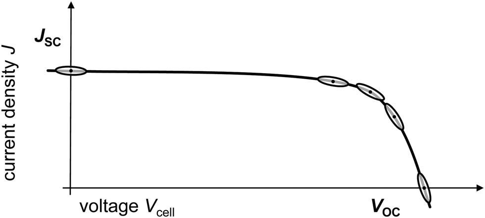 | ||
| Fig. 5 Schematic of a JV curve with possible operating points for IS measurements, VOC, JSC and MPP plus around the MPP. The points within the ellipses signify the essential steady-state operating point and the ellipses themselves indicate the range of voltage and current density that the devices undergo during the IS measurement, respectively. | ||
Phenomenologically, VOC is clearly defined as the operating point where no net current flows, and the device is in quasi-equilibrium. While in principle, all solar cell operating points correspond to a steady-state condition (after a characteristic waiting time), quasi-equilibrium is a particular feature of the VOC. At VOC, all photogenerated charge ultimately recombines radiatively, and all electronic processes, drift, diffusion, charge transfer, are reversible and therefore VOC is a clearly defined operating point for extracting dynamics of electronic processes.63
The current changes sign around VOC during the IS measurement, which has raised concerns whether an impedance spectrum measured at VOC satisfies the condition of reversibility, and if the results are then indicative of the operating point. However, for the small perturbations used in IS, the concept of microscopic reversibility can be applied. The concept is based on Boltzmann kinetics and implies that in equilibrium, forward and backwards processes occur at identical non-zero rates, which means the perturbation does not change the nature of the occurring processes (forward into backwards or vice versa) but just their respective rates. The interested reader is also referred to Butler–Volmer kinetics and the concept of the exchange current density, the “microscopic flux crossing the interface equally in both directions at equilibrium”.64 In other words, VOC is thermodynamically well-defined, and this generally facilitates the interpretation of any experimental parameters extracted at this operating point.
The growing number of reports on accelerated degradation at VOC in PSC highlights the necessity to closely monitor the cell parameters during the experiment, in particular shifting of the DC value of VOC, which will corrupt the IS measurement. On the other hand, non-reversible processes observed at VOC are an excellent indication of stability issues. One has to consider that VOC represents the operating point with the largest electric field inside the device, which can enhance field-dependent processes. This effect can be reduced by using lower light intensities for IS measurements at VOC, in order to reduce the photocurrent density, reduce the VOC, and enhance stability during measurements.65 However, concrete standards are still missing here, such as well-defined intensities and measurement times.
In summary, we recommend IS measurements at VOC, as this is the most well-defined operating point physically.
These measurement issues reflect the underlying physics occurring at JSC. Under these conditions, there is no photovoltage and the solar cell produces no power; the energy levels of the transport layers are short-circuited in the outer circuit and all of the electrical energy is being dissipated as current. Those circumstances hardly vary in the voltage amplitude window used for IS; the line in the “eye” at JSC in Fig. 5 is straight which suggests a linear response, however, it is also flat which indicates that there is little information to be gained from the impedance, which probes the relationship between voltage and current (density). In summary, JSC is not recommended as an operating point for impedance analysis.
It is also worth considering that if FF is approaching unity, i.e. the better the solar cell performance, the more pronounced and the sharper the bend around the MPP gets, which makes an impedance measurement at the MPP even more challenging for the reasons mentioned above.
In summary, performing IS at operating points around the MPP can – in theory – be very helpful to investigate PSC stability and performance. However, this is practically very challenging to do reliably.
The depletion approximation is satisfied if no current flows in the device, which, for solar cells, generally corresponds to dark measurements under reverse bias. However, care must be taken to ensure that unexpected carrier dynamics, due e.g. failure to fully deplete the semiconductor,10 carrier injection under reverse bias,11 or ion migration,66 do not introduce unexpected electrochemical capacitances related to transport dynamics of electrical or ionic carriers. In short, Cf and Mott–Schottky measurements are used to probe the frequency-dependent capacitance of the device, which can be related to electronic structure. Dynamic processes, in particular mobile electronic or ionic species, will result in artefacts in these measurements. In the case of PSC, performing measurements at low temperatures may be a useful approach to limiting artefacts due to ion migration.9,31
Settings for IS on PSC
Proper settings to perform IS measurements are a prerequisite for obtaining reliable spectra, however, the process of choosing suitable settings is rarely addressed in the literature. Here, we provide some practical advice on choosing the excitation signal and amplitude, as well as setting up the measurement procedure.The recommended procedure for identifying a suitable amplitude is to start with a small amplitude and increase it only if the data quality is poor. The increase in voltage amplitude is legitimate if the data quality is improved but the overall shape of the obtained spectrum does not change. Further increase of the averaging (see below) can be performed if the noise is large, and the amplitude cannot be increased, a common issue at low frequencies.
The slowest process in a PSC determines the required waiting time before starting the impedance measurement. To be clear, the waiting time is not determined by the lowest frequency used in the IS measurement but by the slowest dynamic process in the PSC. As a rule of thumb, at least 3τ (τ being the time constant of the slowest process, corresponding to the peak frequency of the respective semicircle in the Nyquist plot) should be considered as standard waiting/equilibration time. If the slowest dynamics are not known, the only way to confirm that the device is in equilibrium is to repeat the measurement under the same conditions and check if the spectra are identical. If not, the waiting time should be increased. For unstable cells, this may not be possible due to irreversible degradation over time, but in that case, an impedance analysis is generally questionable. In the ideal case that the dynamics are known and the measurement frequencies are chosen accordingly to include the slowest dynamics, waiting times of 1/3 of the measurement time are a good default value, for example 10 min waiting time for an impedance measurement that takes 30 min.
Ideally, waiting times for PV devices are determined by electronic processes, which are much faster than the practical times required for setting up and starting the measurement. Therefore, waiting times are practically irrelevant for ideal solar cells. However, in the case of PSC, slow (electro-) chemical processes on much longer timescales can require significant waiting times. In fact, the necessity for waiting times indicates the presence of slow electrochemical processes.
Validity of impedance spectra
Ultimately, a consistent impedance analysis requires reliable spectra. The specific criteria for reliability in IS arise from linear circuit theory:(1) Linearity: linearity of the impedance spectrum is provided if IAC scales linearly with VAC, which means that Z = VAC/IAC is independent of the excitation amplitude. If the amplitude of VAC is too large and exceeds the linear regime, the current response contains higher order harmonics on top of the linear base term. Nonlinear impedance spectra (more specifically, the transfer functions of the higher harmonics) can be analysed, but they require more advanced and non-standard analytical methods than those used to analyse linear impedance spectra. If the spectrum is assumed to be linear, but contains higher harmonics, this can lead to serious errors in the analysis.
(2) Stability: the sample properties do not change during measurement. In other words, impedance spectra are reproducible and successively measured spectra will be identical; the measured system is time invariant.
(3) Causality: the sample response IAC is only due to the VAC excitation and not external factors such as the applied DC voltage, illumination, temperature, or other sources.
(4) Finiteness: impedance values must be finite for finite frequencies.
Violations of any of these criteria mean that standard analysis approaches, such as ECM, will likely not yield useful information reflecting the physical properties of the sample.
For impedance measurements on PSC, the most common issues are low sample stability (or not enough waiting time after a change in operating conditions such as voltage, illumination, temperature), and nonlinearity due to poorly chosen VAC amplitude at the operating point of interest.
The quality of linear impedance spectra can be assessed using the Kramers–Kronig (KK) equations. The KK equations are mathematical relationships that relate the real and the imaginary parts of a complex spectrum. If the transfer function satisfies the criteria of linearity, stability, causality, and finiteness, then the KK relations can be used to calculate the real part of the IS spectrum from the imaginary part, and vice versa. In practice, KK tests are performed on experimental impedance spectra by approximating the KK integrals with a finite chain of resistor–capacitor (RC) elements. This eliminates the challenge of performing the KK integrals (with limits from 0 to infinity) over the finite frequency range of the discrete measurement points (Hz to MHz). The assumption is that an ideal RC circuit is KK compliant, and therefore a chain of RC elements is also KK compliant. Further, any KK compliant impedance spectrum can be fit with a chain of RC elements.67–69 In ref. 67, the test procedure is introduced, while ref. 68 introduces an independent criterion for the number of RC elements to be used for the KK test, and ref. 69 shows that the general assumption of approximability holds true.
The KK test quantifies deviations between the measured and predicted values of the real and imaginary components of the impedance spectrum as the corresponding residuals. It is not possible to generally quantify threshold maximum values for the residuals. In principle, stochastically distributed residuals point towards noise and larger values, i.e. up to 2% might be tolerable, whereas a systematic deviation over a larger frequency range indicates issues with sample stability and measurement reproducibility, even if its maximum deviation is below 0.5%.
In the case of PSC, we have observed that it is not easy to obtain KK-compliant IS spectra. Hysteresis effects in the JV curve combined with limited sample stability make it challenging to find a stable operating point. That underlines the importance to perform KK-tests to confirm that IS spectra are consistent and reliable. It has been shown by the group of Adachi that even PSC showing less than 1% degradation in performance over 1000 hours under operation in light did not show stable impedance spectra at VOC due to reversible polarisation behaviour that occurs over the range of tens of minutes to several hours.70 In fact, the spectra showed an increase of up to four-fold in magnitude during the course of 24 h. However, keeping the sample in the dark for two days resulted in a recovery such that the initial spectrum was restored. In other words, even reversible processes can result in unreliable data if they occur on comparable and longer time scales than the impedance measurement itself.
In PSC, loops and hooks in the IS spectra are frequently reported. These may arise from reproducible physical phenomena or from measurement artefacts likewise. Therefore, it is very important to check the validity of impedance spectra containing such features, either by KK-test or repeat measurements.
Equivalent circuit modelling (ECM)
Equivalent circuit modelling (ECM) is the most common approach to analyse impedance spectra. Equivalent circuit models (ECM, note that the same acronym is commonly used for both equivalent circuit models and equivalent circuit modelling) are necessary to parameterise the IS data by identifying and quantifying relaxation processes from the impedance spectrum. ECM has been applied to emerging photovoltaic devices,9 such as DSSC,13,14,20 OPV.15,16 More recently, there has been a great interest and progress in establishing ECM for PSC,20–23,65 but there are still many open questions to be addressed with regards to a universal, physically motivated ECM for PSC. In the following section, we propose a framework to derive a generalised ECM for PSC and discuss it with respect to other models found in the literature. In this section, we provide a short introduction on the basics of ECM.ECM relies on the assumption that relaxation processes are first order, reversible, and independent phenomena, such as charge transport, charge transfer, charge recombination, and simple chemical reactions. This means that these phenomena can be modelled independently from each other, that impedance spectra are necessarily reproducible, and the spectra themselves are time-independent. In this case, the impedance spectra can be modelled using an ECM composed of a combination of ideal, linear circuit elements with fixed values. The RC element (Fig. 3c) introduced previously is the basic ECM building block for modelling relaxation processes. In practice, most relaxation processes appear in the spectrum as dispersive relaxation processes with more than one time constant, in other words, a distribution of time constants. That can be due to inhomogeneity in sample quality (e.g. surface roughness) or operating conditions (e.g. temperature), or it can be caused by a concrete dispersive process (e.g. charge transfer at porous electrodes or electrical transport in amorphous semiconductors). Often, dispersive relaxation processes can be modelled by an RQ circuit, in other words, the C in the parallel RC element is replaced by a constant phase element (CPE). For other specific cases, specific circuit elements are used, such as the Warburg element for mass transport. A detailed introduction into the different circuits can be found elsewhere.3,48,71
At this point we would like to emphatically note that an ECM does not necessarily represent a unique solution to an impedance spectrum. It has often been shown in IS literature that very different ECMs produce identical frequency responses, and therefore, there may be several ECMs that can reproduce a single experimental impedance spectrum. Therefore, an ECM should ideally fulfil two basic requirements. First, it must accurately reproduce (without systematic error) the dynamic and steady-state electrical behaviour of the device at the DC operating point of measurement over the full IS frequency range. However, generally there is a range of models that will satisfy this criterion, and the different circuit structures and arrangements lead to different quantities for the parameter values, and therefore ambiguity in the physical interpretation. Therefore, the second more rigorous requirement for the ECM is that it must contain relevant, quantified, and unambiguously extractable parameters for the analysis.
ECMs in the PSC literature have focused mainly on the first requirement to date. The second requirement is more challenging, and it might even be impossible to fulfil it to its finest detail for PSC because of:
• The large number of dynamic processes (transport, recombination, electrode processes, ionic/electronic processes, reactions at the interfaces, trapping/de-trapping) that (sometimes) overlap in the impedance spectrum leading to multiple different ECMs that can reproduce the same IS response.
• The interdependencies of processes, such as carrier transport, recombination, and electrochemical dynamics make it difficult to obtain reliable spectra and/or unequivocally assign individual IS signatures.
• Instable electrical properties lead to unreliable IS spectra that are either KK incompliant or not reproducible, or both.
With this introduction to ECM, we aim to underline the difficulties in finding an appropriate ECM, which is one of the main reasons that the ECM is still under discussion in the community. However, we will show how one can apply available knowledge about dynamic processes in PSC in order to identify relevant behavioural traces and parameter values by IS. In the next section we will develop and derive an empirical foundation for a versatile PSC model, which can be adapted for most types of PSC.
ECMs are very handy for quantifying the resistive and capacitive signatures, and for extracting the timescales, of well-known and/or ideal processes. In this case, ECM provides a global model consisting of simple, well-defined circuit elements that can be used to parameterise the system. One way to design an ECM is to start with the relevant set of differential equations that describe the basic device physics in the ideal system. This approach, however, may neglect non-ideal and unexpected effects observed in real samples. In fact, these non-ideal processes are often related to performance and stability losses, and therefore very relevant for many IS studies. For example, in ref. 72 an ECM for Lithium ion batteries was established, and when interpreting features of the spectra, the researchers concluded that, contrary to the initial assumptions, one of the main semicircles in the spectra was due to a contact resistance between cathode and current collector. Analogously, in the case of solar cells, the effects of contacts (blocking, recombination, series resistances) are neglected in more idealised models.
Performing ECM on unknown samples can lead to ambiguous results when attempting to attribute circuit elements to uncharacterised physical processes. For example, interfacial charge transfer, charge recombination, and chemical reactions may result in similar impedance signatures, although the physical origins and implications on device performance are very different. Also, assuming that processes occurring in parallel or sequentially – and modelling them correspondingly – will lead to different ECMs and different parameter dependencies. Our suggestion for best practice for assigning unknown IS signatures is therefore to perform corroborative measurements to determine the underlying physical origin.
Specifically, in the case of PSC, the exact processes that determine device performance, and their dependence on the solar cell operating conditions, are still elusive. Due to the co-existence of both electrical and electrochemical dynamics, PSC present a few new challenges to impedance analysis that have not been apparent for other types of solar cells.28,29,39,40 Therefore, we argue that an empirical approach may actually help in this case to shed light on unknown or non-ideal processes in these devices.
Generalised equivalent circuit model for perovskite solar cells
Here, we aim to develop a general platform for an adaptable ECM for PSC that can account for the different IS features observed in the literature (see Fig. 1), while providing a set of parameters for the features that are common to all spectra measured on PSC. We see this as a helpful contribution towards fulfilling the requirement that ECMs contain relevant, quantified, and extractable parameters, as discussed in the previous section. Specifically, we propose an ECM that consists of an HF component to describe the known fast electrical dynamics in PSC (Fig. 2) combined with a variable LF component to describe the range of possible electrochemical dynamics observed in PSC. This flexible platform is based on a physically motivated ECM to describe both electrical and electrochemical processes, combined with the flexibility to adjust the LF response according to the specifics of the PSC and its measurement conditions.We begin by considering the impedance response in terms of the HF and LF signatures to provide a physically motivated ECM that accounts for what is currently considered substantiated knowledge in the literature for dynamics in PSC (see Fig. 2).
For the reasons outlined in the previous section, we base our ECM on IS spectra measured at VOC under standard solar light irradiation, but this approach is applicable to other operating points as well.
Separating HF and LF features in a general ECM
As shown in Fig. 1 and 2, the impedance response of PSC can be divided into HF and LF contributions that are separated from each other by several orders of magnitude in the frequency spectrum.To put our approach into context with previous work, the ECM structure shown in Fig. 6 represents one of the commonly reported physically motivated structures, the derivation of which is detailed in many studies.27,73,74 The part of the ECM describing the processes within the absorber layer (brown layer in Fig. 6), the transport layers (red and green in Fig. 6) and the interfaces are branched out, which leads to a nested circuit (or in special cases to a circuit referred to as Matryoshka circuit26). In the nested circuit, the elements representing the HF and LF impedance are located where they phenomenologically occur in the device, and the underlying (differential) equations are derived based on the physical understanding of the device. In principle, this is a logical approach that is intended to reflect the device physics and reproduce the IS data. However, the resulting structure of nested circuits is much more complex than a series connection of circuit elements, even though it has been shown that for PSC the parameter values for both nested and linear ECMs are very similar.26,75 Nested circuits are difficult to parametrise, the fitting procedure becomes unstable for multiple branches, and the fitting values can be difficult to rationalise as the simple relationship τ = RC for the time constant no longer applies. More universal, simple structures generally lead to more reproducible fit results.
 | ||
| Fig. 6 Schematic with series resistance R0, high-frequency resistance RHF, and a potential LF feature. Grey and yellow rectangles represent the current collectors, and the brown, red and green layers represent the absorber and transport layers, respectively. | ||
In the following, we will present a rational detailing why such branching or nested circuits are not necessary for PSC. Namely, the characteristic frequencies of the HF and LF impedance signatures are separated by at least two orders of magnitude in the frequency domain. This makes it possible to decouple signatures in the HF and LF regime, enabling a series model, which is easier to handle, to parametrise, and to rationalise. Recent studies combining impedance spectroscopy with drift-diffusion modelling have applied an analogous approach to derive recombination dynamics and the solar cell ideality factor from PSC from the HF signature.76,77 This demonstrates that empirically-derived ECMs can be used to extract relevant PSC parameters.
The approach is based on one central assumption: that the geometrical capacity Cgeo of the PSC does not affect the LF impedance. By relying on this assumption, we gain the desired flexibility in the ECM, such that we can separate the ECM in a HF-ECM and a LF-ECM without changing the parameters for the respective circuit elements. Another outcome of these considerations is the confirmation that the series resistance can be assigned unequivocally to the Ohmic resistance originating from the current collectors.
In order to verify our central assumption, and to demonstrate the impact of Cgeo on the HF impedance, we introduce a hypothetical model, which consists of a series resistance and three RC elements or (perfect) semicircles. We simulated this hypothetical ECM from 10−3 Hz to 1014 Hz with 250 data points. The parameter values of the individual elements are chosen as such that there are two fast processes (red and yellow) and one slow process (green). This results in a Nyquist plot analogous to those reported for PSC in the literature (Fig. 1). The two fast processes represent electrical relaxation processes such as transport and recombination, while the third process represents one slow electrochemical process, consistent with the different dynamics observed in PSC depicted in Fig. 2. The large data points in the spectra mark (local) negative maxima in the imaginary part of the impedance indicating the characteristic frequency, fchar, respectively. We now demonstrate how a finite value of Cgeo (which is in parallel to all electrical and electrochemical dynamics) impacts the IS signature of the faster processes, but not the slow one.
For a successive increase of Cgeo from zero, the following can be observed in Fig. 7:
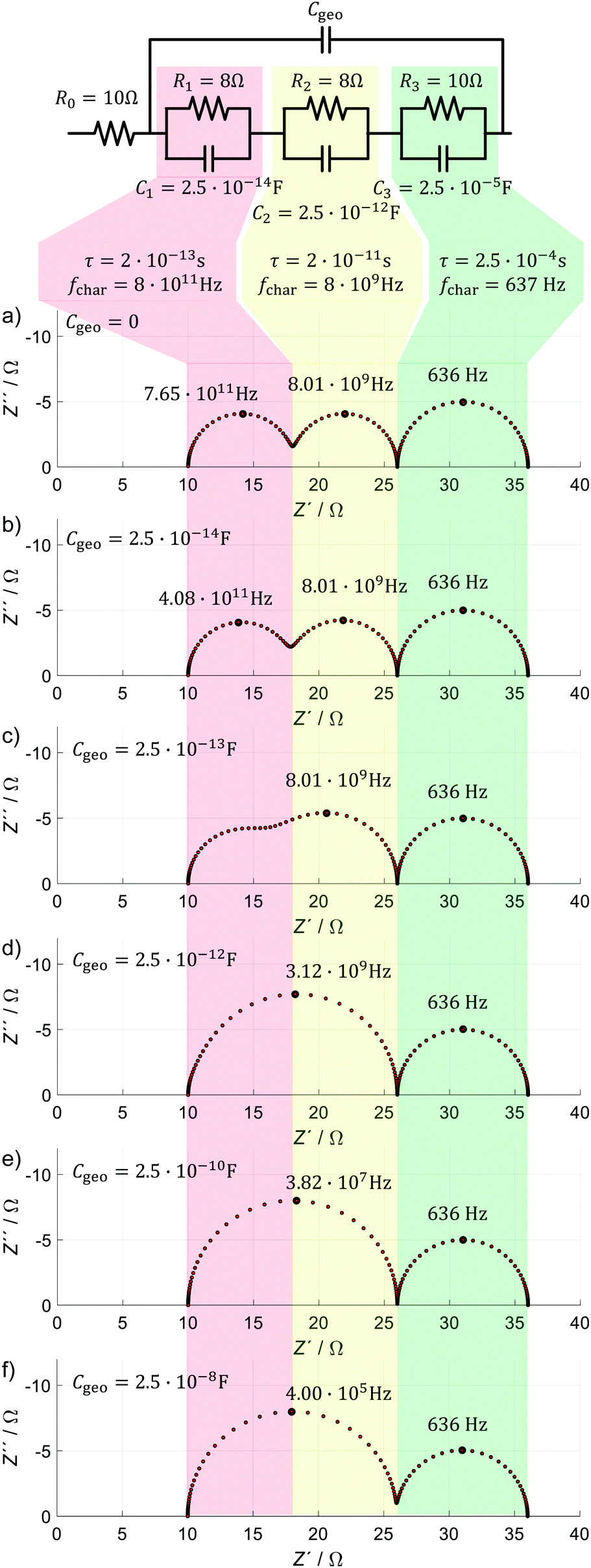 | ||
| Fig. 7 Demonstration of the impact of Cgeo on the IS response with the help of a hypothetical equivalent circuit model (ECM). On top, the model structure is shown together with the parameter values including time constant τ and characteristic frequency fchar. The impedance spectra show simulations for different values of Cgeo varying from 0 to 2.5 × 10⁻⁸ F in 6 steps. The color code highlights the fastest process in light red, the second fastest in light yellow and the slow process in light green. All values are hypothetical but chosen to be close to the area-specific resistances and capacities of a planar PSC under illumination at VOC. | ||
(a) Cgeo = 0: all three processes are visible by the respective semicircles, and the large data points mark the expected values for fchar with good accuracy.
(b) Cgeo = 2.5 × 10⁻¹⁴ F: the semicircles of the two fast processes begin to merge, and notably fchar of the red process decreases by a factor of ∼2.
(c) Cgeo = 2.5 × 10⁻¹³ F: the semicircles associated with the two fast processes further merge, and fchar of the yellow and green processes still remain unchanged.
(d) For Cgeo = 2.5 × 10⁻¹² F: the semicircles associated with the two fast processes merge completely and fchar of the single remaining fast process decreases by a factor of ∼2.5.
(e) For Cgeo = 2.5 × 10⁻¹⁰ F: the shape of the impedance spectrum does not change significantly anymore, but fchar of the single fast process decreases by almost two orders of magnitude, the same magnitude with which Cgeo increases.
(f) For Cgeo = 2.5 × 10⁻⁸ F: fchar further decreases by almost two orders of magnitude, similarly to the increase in Cgeo.
With this simple demonstration, we see how Cgeo slows down the response of the fast processes in the simulated spectra, causing the HF semicircles to merge into a single semicircle with a significantly decreased fchar. This happens when Cgeo is significantly larger than C1 and C2. In this case, C1 and C2 do not influence the dynamics of the ECM at all. Practically speaking, Cgeo will therefore mask any faster impedance signature in the PSC. This is because no current flows through C1 and/or C2 at high frequencies (for Cgeo > 2.5 × 10⁻¹⁰ F and a test frequency f (= ω/2π) > 10 kHz: ZCgeo ≪ ZC2 < ZC1 < ZC1+C2).
But why do we still see a series resistance in all simulated spectra in simulated spectra in Fig. 7? The above considerations are only true for processes that are geometrically located inside the PSC, i.e. that are in parallel to Cgeo, representing the plate capacitor defined by the current collectors in Fig. 6. That is the reason that the very fast impedance of the current collectors (R0 in Fig. 6), can be distinguished from the processes “inside” the device (vertical processes in Fig. 6) with IS. In turn, the results of this simulation confirm that R0 can be attributed to current collectors and electrical contacts, and that it is sensible to model it as a series resistance. It cannot represent any process inside the cell structure, such as a residual Ohmic resistance of the perovskite or contact layers, because in this case it would be dependent on the value of Cgeo.
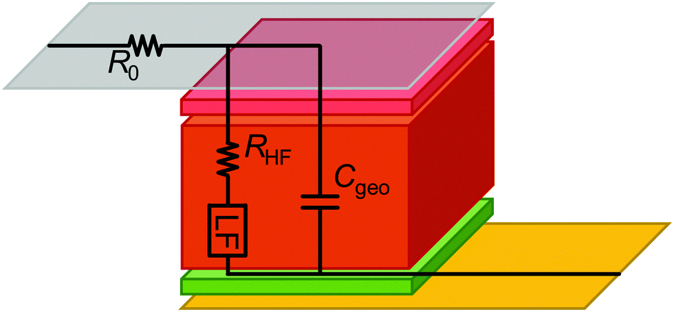
In all simulations, the slow process (green) is not influenced by changes in Cgeo. This is because the timescale associated with the slow dynamics is several orders of magnitude larger than those of the (merged) fast processes. The reason for this can be found in the capacitance of the respective RC circuit, which is three orders of magnitude larger than the largest simulated Cgeo. In this case, it is essentially irrelevant if the geometrical capacity is in parallel or in series with the LF circuit elements. Therefore, we propose to simplify the ECM structure as shown in Fig. 8, and include the LF signature as a separate element in series to the HF features.
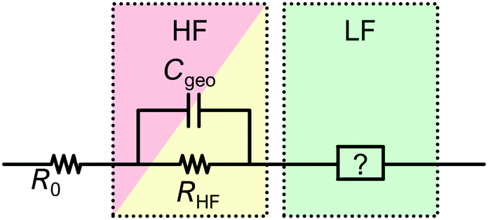 | ||
| Fig. 8 General structure of the proposed ECM. R0 accounts for the Ohmic resistance of the contacts and current collectors, Cgeo is the geometrical capacity, RHF is the sum of all HF features in the spectrum and the LF-ECM will be detailed below. | ||
In summary, according to Fig. 8, Cgeo is the only capacitance that is practically relevant for IS on PSC in the high frequency regime, while it is not relevant for the low frequency regime. As detailed in many studies, there are several other capacitances that can contribute to the HF signature. However, as capacitances related to charge transport are parallel to Cgeo, their contribution to the total HF signature is negligible and they cannot be identified or quantified from the IS data. Therefore, it is not helpful to include those in this general structure for the ECM. One exception is the chemical capacitance (eqn (12)) which arises due to charge injection in the depleted semiconductor, and is in series with Cgeo. However, as we have already noted above, this capacitance is only relevant for PSC in depletion mode,78i.e. for defect spectroscopy studies which are not analysed using ECM.
The sum of all resistances in the high frequency regime (RHF) results from multiple contributions, such as recombination and transport resistances (see Fig. 2). For the model in Fig. 7, RHF = R1 + R2. All contributions to RHF are additive. This holds whether the resistive contributions are independent (truly in series) or interdependent (e.g. both depend on carrier density, such as transport and recombination). A major consequence of this is that RHF cannot be deconvoluted into the individual resistive components from a single impedance spectrum. Only by varying the operating conditions, materials or the cell configuration systematically, is it possible to potentially access to individual contributions.
General ECM – LF
The LF signature probed by IS on PSC is very characteristic, and often, several distinct features are observed in the spectra. On the other hand, the LF signature varies significantly for different cells and, from the literature, it is nearly impossible to define a standard LF signature, such that it is almost impossible to formulate a single general ECM for the LF regime.The slow dynamics cannot be explained by purely electronic processes, and it is generally agreed that these are related to (photo)electrochemical processes. The dynamics are slow because they either represent slow reactions or transport, or because they represent faster processes that are modulated or limited by sluggish ion and vacancy migration or slow reactions. One major point of contingency is the variation between diverse positive and negative semicircles, which also appear as loops and hooks, in Nyquist plots reported in the literature. We propose a general description that accounts for all potentially occurring phenomena.
According to the current understanding of PSC, the following processes are likely to happen due to slow changes in the applied electric field, such as during the IS excitation at low frequencies. Ions and vacancies drift due to the slowly changing electric field. The contacts however, block the ions and vacancies, so that there is an electrical current but no net ionic current. This leads to electrode polarisation which means that ions and/or vacancies accumulate or deplete at a given electrode interface, thereby changing the internal field in the PSC. Possible consequences are:
(a) changes in the electrical drift and diffusion currents under a constant DC bias due to the change in electrostatic potential in the PSC and the accumulation or depletion of ions, vacancies or polar molecules,
(b) triggering of chemical reactions due to the change in ion density and/or local field,
(c) formation of traps, and/or.
(d) neutralisation of existing traps.
The question is how these processes impact the IS data and result in the diverse LF signatures. We now consider the possibilities for ion or vacancy migration and other reactions during the AC time interval of the excitation in the low frequency region. However, we do not consider the ionic migration itself – assumed to have a small impact because of the limited number of charges involved – but instead the resulting impact of the migration on the electrical properties.39,40 For the sake of simplicity, we describe those possibilities in the text and in Fig. 9 only for the part of the oscillation when the voltage increases. The IS response is assumed to be (pseudo-) linear due to the small perturbation about equilibrium, and therefore all processes are assumed to be completely reversible:
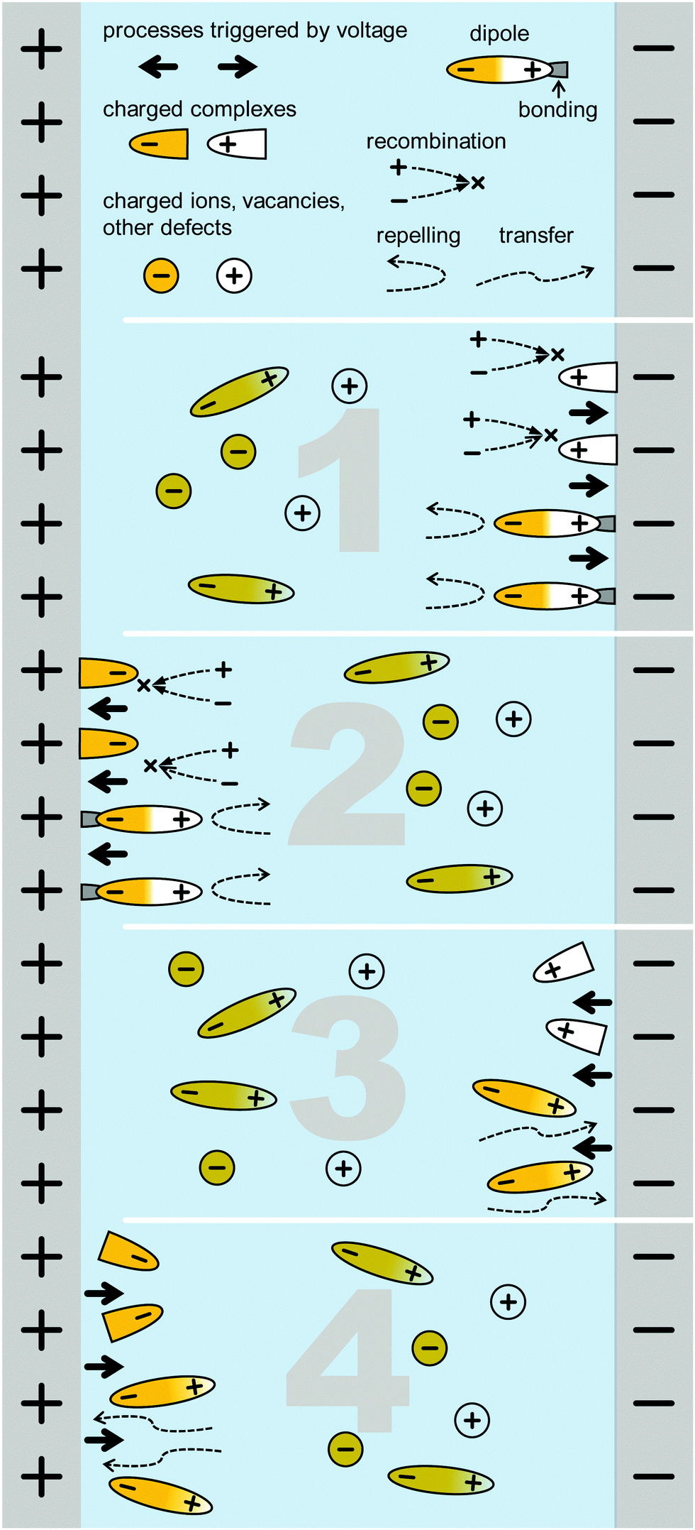 | ||
| Fig. 9 Schematic of a cell structure with positively and negatively charged ions/vacancies that are supposed to drift due to the outer electric field. At the contacts, those can bond or react at the interface, either foring recombinations centers or, oppositely, passivating the interface. Bonding or electrochemical reaction products bound to the interfaces are symolised by the posts on the respective electrodes. Numbers indicate the number of the list of possible scenarios for field-driven effects described in the text. | ||
1. positively charged species (ions, vacancies or polar molecules) accumulate at the “–” side, resulting in recombination centres or electrode polarisation leading to ion accumulation leading to hindrance of charge transport and transfer,
2. negatively charged species (ions, vacancies or polar molecules) accumulate on the “+” side, resulting in recombination centres or electrode polarisation leading to hindrance of charge transport and transfer,
3. negatively charged species are repelled from the “−” side, which neutralise existing recombination centres or improves the transport or transfer of charges,
4. positively charged species are repelled from the “+” side, which neutralise existing recombination centres or improves the transport or transfer of charges.
We note that Scenarios 1 and 2, and Scenarios 3 and 4 cannot be distinguished as the impact is qualitatively equal, but may indeed result in distinct signatures in IS. Scenarios 1 and 2 both result in a positive resistance and a time constant. It is possible to calculate a capacitance from these values (C = τ/R), which will be positive and will either be a double-layer capacitance (in case of an electrochemical reaction as the limiting factor) or a chemical capacitance (in case of the ion migration as the limiting factor).
Scenarios 3 and 4, on the other hand, result in a negative resistance and a positive time constant. This is because the impact from the corresponding limiting factor (recombination and/or poor charge transfer) decreases with increasing voltage at low frequencies. The increase in current due to both the increasing voltage and due to the elimination of limiting factors, representing what has been described as “negative differential resistance (NDR)”. The time constant will still be positive because causality in the system prevails. The corresponding capacitance can be calculated as in the case of Scenarios 1 and 2, but it will adopt a negative value. The reason is that the capacitive element is actually discharged during the phase when the voltage increases, as schematically depicted in Fig. 9. Negative capacitance may be represented by an inductivity, however, this results in a different ECM structure.59
These two cases, scenario 1/2 and scenario 3/4 describe related physical processes, but lead to different IS features depending on whether the electrochemical processes enhances or limits current transport during the AC oscillation. This difference can explain the emergence of the different low frequency features, such as loops and hooks, in different spectra reported in the literature. From the opposite perspective – identifying the physical effect from the impedance spectrum – is not possible, as there is still not enough knowledge available about the underlying electrochemical processes to provide a general recipe to elucidate the physical nature of LF signatures based on the impedance response alone. More specifically, from the shape alone, it is impossible to distinguish between the different scenarios (1/2 or 3/4), and also to identify which type of charge carrier is affected as well as potential reactions. That can be done successively by thoroughly measuring and calculating the respective mobilities and activation energies, dedicated materials testing experiments with predominant mobile species, and specifically tailored IS or conductivity measurements.
The LF part of our suggested ECM (Fig. 10) is constructed according to the possible number and nature of processes occurring. Here we remind the reader that the HF part of the ECM is well-defined as it is determined by the electrical processes, and ultimately dominated by Cgeo. In contrast, the LF part of the ECM depends on specific electrochemical processes, which in turn depend on specific PSC architectures and the measurement conditions. Therefore, the LF-ECM is necessarily empirical because of the current lack of knowledge of the electrochemical processes occurring in different PSC at different solar cell operating points. Therefore, it is fundamentally not possible to design a universal LF-ECM that naturally accounts for all LF features in the IS of PSC. On the other hand, an empirical description of the impedance spectrum is an important step towards gaining a full understanding of the processes in PSC, and a very helpful tool to monitor parameter evolution over time, particularly during stability tests. Our proposed ECM, which combines the physically motivated HF-ECM and the empirical LF-ECM, offers researchers a simple tool box to study PSC stability, and specifically elucidate how the electrochemical processes described in Fig. 9 impact the HF-response and result in different LF features in the Nyquist plot, such as loops and hooks.
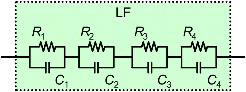 | ||
| Fig. 10 Possible structure of the LF ECM employing all four options mentioned in the text. | ||
This approach is intended as a first step to create a framework for a general description. We follow the approach in the work by Lasia79 (Section 5.3), where the adsorption of several species is modelled on top of an electrochemical reaction at a solid–gas interface. In this case, the author depicts a nested circuit but indicates that other ECM structures are possible. As there is currently no substantial information about the LF processes and their interdependencies available, we propose the simplest approach – a linear circuit – that can account for the respective number of features in the spectrum. Also, only a series connection of the (optional) features in Fig. 10 makes it possible to evaluate the characteristic parameters, such as resistance, capacitance and time constant, of these processes independently. This is helpful for a more in-depth physical interpretation of the observed phenomena.
For the sake of simplicity, the all ECMs introduced here include capacitors. For real IS data, capacitors may be substituted by constant phase elements to enable accurate fitting. It is worth mentioning that the quality of the fit is best assessed via the residuals plot – Nyquist or Bode plots alone are generally too coarse for a reliable judgement.
The approach presented here differs from most ECM approaches for PSC in the literature. Those can be put into two categories, the first being physically motivated ECMs that account, as closely as possible, for the device physics but place less focus on what is likely, possible, and practical to probe with IS. This approach fails to provide a general framework to understand the varying LF impedance – which is, admittedly, almost impossible to elucidate with IS with the current understanding of the devices, materials, and chemical reactions. In the second category, there are empirical ECMs that try to account for the visible features in the spectra and then attempt a physical interpretation of these features. Our contribution here represents a useful compromise by starting with the device physics, namely the known timescales for dynamics in PSC; and then simplifying the ECM by decoupling the HF and the LF regimes. That enables us to have a closer and unbiased look (independent from the HF impedance) at the LF impedance in order to gain better insights into the unknown, non-ideal electrochemical processes, and their corresponding IS signatures, that cannot be expressed in terms of basic equations that govern solar cell physics.
Conclusions
Impedance spectroscopy (IS) is a powerful tool for operando characterisation and diagnosis of perovskite solar cells (PSC). However, to date, universal models for IS from PSC have been elusive. Based on the current understanding of electrical and electrochemical dynamics in PSC combined with relevant IS basics, we propose a universal approach for equivalent circuit modelling (ECM) for PSC. Our model serves as an up-to-date platform for the unambiguous analysis of IS on different PSC, and provides a straightforward approach for the diagnosis of critical loss processes. Our simplified ECM structure deconvolutes fast electrical processes from slow electrochemical processes along with a comprehensive explanation and parameter assignment for the HF component. We highlight that although the LF and HF signatures can be modelled independently, there is an obvious interdependence between the electronic and electrochemical dynamics in a PSC. Therefore, monitoring how the LF regime relates to the HF signature can yield valuable insight into how electrochemical dynamics determine and limit electrical transport, and therefore photovoltaic performance in PSC. We recommend that researchers who aim to improve PSC stability focus on eliminating LF signatures because those are mostly linked to detrimental non-ideal processes.Conflicts of interest
There are no conflicts to declare.Acknowledgements
We want to thank Dr G. Tumen-Ulzii, Prof. T. Matsushima and Prof. C. Adachi (Center for Organic Photonics and Electronics Research (OPERA), Kyushu University) as well as Mischa Hillenius, Mees Dieperink, and Tulus for very helpful discussions. D. K., acknowledges funding from Kakenhi Grant-In-Aid for young scientists, grant number 18K13993/20K15028.References
- A. K. Jena, A. Kulkarni and T. Miyasaka, Chem. Rev., 2019, 119, 3036–3103 CrossRef CAS PubMed.
- M. V. Khenkin, E. A. Katz, A. Abate, G. Bardizza, J. J. Berry, C. Brabec, F. Brunetti, V. Bulović, Q. Burlingame, A. Di Carlo, R. Cheacharoen, Y. B. Cheng, A. Colsmann, S. Cros, K. Domanski, M. Dusza, C. J. Fell, S. R. Forrest, Y. Galagan, D. Di Girolamo, M. Grätzel, A. Hagfeldt, E. von Hauff, H. Hoppe, J. Kettle, H. Köbler, M. S. Leite, S. (Frank) Liu, Y. L. Loo, J. M. Luther, C. Q. Ma, M. Madsen, M. Manceau, M. Matheron, M. McGehee, R. Meitzner, M. K. Nazeeruddin, A. F. Nogueira, Ç. Odabaşı, A. Osherov, N. G. Park, M. O. Reese, F. De Rossi, M. Saliba, U. S. Schubert, H. J. Snaith, S. D. Stranks, W. Tress, P. A. Troshin, V. Turkovic, S. Veenstra, I. Visoly-Fisher, A. Walsh, T. Watson, H. Xie, R. Yıldırım, S. M. Zakeeruddin, K. Zhu and M. Lira-Cantu, Nat. Energy, 2020, 5, 35–49 CrossRef.
- V. F. Lvovich, Impedance Spectroscopy: Applications to Electrochemical and Dielectric Phenomena, John Wiley & Sons, 2012 Search PubMed.
- J. T. S. Irvine, D. C. Sinclair and A. R. West, Adv. Mater., 1990, 2, 132–138 CrossRef CAS.
- E. Ivers-Tiffée and A. Weber, J. Ceram. Soc. Jpn., 2017, 125, 193–201 CrossRef.
- D. Abou-Ras, T. Kirchartz and U. Rau, Advanced Characterization Techniques for Thin Film Solar Cells, 2nd edn, 2016, vol. 1–2 Search PubMed.
- S. Reichert, J. Flemming, Q. An, Y. Vaynzof, J. F. Pietschmann and C. Deibel, Phys. Rev. Appl., 2020, 13, 034018 CrossRef CAS.
- T. Walter, R. Herberholz, C. Müller and H. W. Schock, J. Appl. Phys., 1996, 80, 4411–4420 CrossRef CAS.
- E. von Hauff, J. Phys. Chem. C, 2019, 123, 11329–11346 CrossRef CAS.
- L. Xu, J. Wang and J. W. P. Hsu, Phys. Rev. Appl., 2016, 6, 064020 CrossRef.
- S. Ravishankar, T. Unold and T. Kirchartz, Science, 2021, 371, eabd8014 CrossRef CAS PubMed.
- J. Bisquert, Phys. Chem. Chem. Phys., 2003, 5, 5360–5364 RSC.
- M. Adachi, M. Sakamoto, J. Jiu, Y. Ogata and S. Isoda, J. Phys. Chem. B, 2006, 110, 13872–13880 CrossRef CAS PubMed.
- Q. Wang, J. E. Moser and M. Grätzel, J. Phys. Chem. B, 2005, 109, 14945–14953 CrossRef CAS PubMed.
- J. I. Basham, T. N. Jackson and D. J. Gundlach, Adv. Energy Mater., 2014, 4, 1400499 CrossRef.
- B. Ecker, H. J. Egelhaaf, R. Steim, J. Parisi and E. Von Hauff, J. Phys. Chem. C, 2012, 116, 16333–16337 CrossRef CAS.
- P. P. Boix, G. Garcia-Belmonte, U. Muñecas, M. Neophytou, C. Waldauf and R. Pacios, Appl. Phys. Lett., 2009, 95, 233302 CrossRef.
- B. Ecker, J. C. Nolasco, J. Pallarés, L. F. Marsal, J. Posdorfer, J. Parisi and E. Von Hauff, Adv. Funct. Mater., 2011, 21, 2705–2711 CrossRef CAS.
- A. Kojima, K. Teshima, Y. Shirai and T. Miyasaka, J. Am. Chem. Soc., 2009, 131, 6050–6051 CrossRef CAS PubMed.
- F. Fabregat-Santiago, G. Garcia-Belmonte, I. Mora-Seró and J. Bisquert, Phys. Chem. Chem. Phys., 2011, 13, 9083–9118 RSC.
- I. Zarazua, G. Han, P. P. Boix, S. Mhaisalkar, F. Fabregat-Santiago, I. Mora-Seró, J. Bisquert and G. Garcia-Belmonte, J. Phys. Chem. Lett., 2016, 7, 5105–5113 CrossRef CAS PubMed.
- A. Guerrero, G. Garcia-Belmonte, I. Mora-Sero, J. Bisquert, Y. S. Kang, T. J. Jacobsson, J. P. Correa-Baena and A. Hagfeldt, J. Phys. Chem. C, 2016, 120, 8023–8032 CrossRef CAS.
- A. Pockett, G. E. Eperon, N. Sakai, H. J. Snaith, L. M. Peter and P. J. Cameron, Phys. Chem. Chem. Phys., 2017, 19, 5959–5970 RSC.
- D. Pitarch-Tena, T. T. Ngo, M. Vallés-Pelarda, T. Pauporté and I. Mora-Seró, ACS Energy Lett., 2018, 3, 1044–1048 CrossRef CAS.
- K. Miyano, M. Yanagida and Y. Shirai, Adv. Energy Mater., 2020, 10 Search PubMed.
- A. Todinova, L. Contreras-Bernal, M. Salado, S. Ahmad, N. Morillo, J. Idígoras and J. J. A. Anta, ChemElectroChem, 2017, 4, 2891–2901 CrossRef CAS.
- S. M. Yoo, S. J. Yoon, J. A. Anta, H. J. Lee, P. P. Boix and I. Mora-Seró, Joule, 2019, 3, 2535–2549 CrossRef CAS.
- M. T. Neukom, A. Schiller, S. Züfle, E. Knapp, J. Ávila, D. Pérez-Del-Rey, C. Dreessen, K. P. S. Zanoni, M. Sessolo, H. J. Bolink and B. Ruhstaller, ACS Appl. Mater. Interfaces, 2019, 11, 23320–23328 CrossRef CAS PubMed.
- D. Moia, I. Gelmetti, P. Calado, W. Fisher, M. Stringer, O. Game, Y. Hu, P. Docampo, D. Lidzey, E. Palomares, J. Nelson and P. R. F. Barnes, Energy Environ. Sci., 2019, 12, 1296–1308 RSC.
- C. M. Wolff, P. Caprioglio, M. Stolterfoht and D. Neher, Adv. Mater., 2019, 31, 1902762 CrossRef CAS PubMed.
- M. H. Futscher, J. M. Lee, L. McGovern, L. A. Muscarella, T. Wang, M. I. Haider, A. Fakharuddin, L. Schmidt-Mende and B. Ehrler, Mater. Horiz., 2019, 6, 1497–1503 RSC.
- M. B. Johnston and L. M. Herz, Acc. Chem. Res., 2016, 49, 146–154 CrossRef CAS PubMed.
- F. Staub, H. Hempel, J. C. Hebig, J. Mock, U. W. Paetzold, U. Rau, T. Unold and T. Kirchartz, Phys. Rev. Appl., 2016, 6, 044017 CrossRef.
- J. Wu, Y. Li, Y. Li, W. Xie, J. Shi, D. Li, S. Cheng and Q. Meng, J. Mater. Chem. A, 2021, 9, 6382–6392 RSC.
- Y. Yang, M. Yang, D. Moore, Y. Yan, E. Miller, K. Zhu and M. Beard, Nat. Energy, 2017, 1–7 Search PubMed.
- C. Wehrenfennig, G. E. Eperon, M. B. Johnston, H. J. Snaith and L. M. Herz, Adv. Mater., 2014, 26, 1584–1589 CrossRef CAS PubMed.
- E. M. Hutter, J. J. Hofman, M. L. Petrus, M. Moes, R. D. Abellón, P. Docampo and T. J. Savenije, Adv. Energy Mater., 2017, 7, 1602349 CrossRef.
- D. Luo, R. Su, W. Zhang, Q. Gong and R. Zhu, Nat. Rev. Mater., 2019, 5, 44–60 CrossRef.
- Z. S. Wang, F. Ebadi, B. Carlsen, W. C. H. Choy and W. Tress, Small Methods, 2020, 4, 2000290 CrossRef CAS.
- G. Y. Kim, A. Senocrate, T. Y. Yang, G. Gregori, M. Grätzel and J. Maier, Nat. Mater., 2018, 17, 445–449 CrossRef CAS PubMed.
- S. Reichert, Q. An, Y. W. Woo, A. Walsh, Y. Vaynzof and C. Deibel, Nat. Commun., 2020, 11, 6098 CrossRef CAS PubMed.
- E. Velilla, F. Jaramillo and I. Mora-Seró, Nat. Energy, 2021, 6, 54–62 CrossRef CAS.
- M. H. Futscher and J. V. Mili, Front. Energy Res., 2021, 9, 1–9 Search PubMed.
- T.-Y. Yang, G. Gregori, N. Pellet, M. Grätzel and J. Maier, Angew. Chem., Int. Ed., 2015, 54, 7905–7910 CrossRef CAS PubMed.
- W. Shockley and H. J. Queisser, J. Appl. Phys., 1961, 32, 510–519 CrossRef CAS.
- L. Bertoluzzi, R. S. Sanchez, L. Liu, J. W. Lee, E. Mas-Marza, H. Han, N. G. Park, I. Mora-Sero and J. Bisquert, Energy Environ. Sci., 2015, 8, 910–915 RSC.
- A. K. Jonscher, Nature, 1977, 263, 673–679 CrossRef.
- J. R. Macdonald, Theory, Experiment, Wiley, 2nd edn, 1995 Search PubMed.
- J. Jamnik and J. Maier, Phys. Chem. Chem. Phys., 2001, 3, 1668–1678 RSC.
- H. Schichlein, A. C. Müller, M. Voigts, A. Krügel and E. Ivers-Tiffée, J. Appl. Electrochem., 2002, 32, 875–882 CrossRef CAS.
- A. A. Bakulin, O. Selig, H. J. Bakker, Y. L. A. Rezus, C. Müller, T. Glaser, R. Lovrincic, Z. Sun, Z. Chen, A. Walsh, J. M. Frost and T. L. C. Jansen, J. Phys. Chem. Lett., 2015, 6, 3663–3669 CrossRef CAS PubMed.
- A. Poglitsch and D. Weber, J. Chem. Phys., 1987, 87, 6373 CrossRef CAS.
- J. Fleig and J. Maier, J. Am. Ceram. Soc., 2004, 82, 3485–3493 CrossRef.
- Z. Hens and W. P. Gomes, J. Electroanal. Chem., 1997, 437, 77–83 CrossRef CAS.
- J. E. A. M. van den Meerakker, J. J. Kelly and P. H. L. Notten, J. Electrochem. Soc., 1985, 132, 638–642 CrossRef CAS.
- D. P. Almond and C. R. Bowen, J. Phys. Chem. Lett., 2015, 6, 1736–1740 CrossRef CAS PubMed.
- E. J. Juarez-Perez, R. S. Sanchez, L. Badia, G. Garcia-Belmonte, Y. S. Kang, I. Mora-Sero and J. Bisquert, J. Phys. Chem. Lett., 2014, 5, 2390–2394 CrossRef CAS PubMed.
- S. Luryi, Appl. Phys. Lett., 1988, 52, 501 CrossRef.
- D. Klotz, Electrochem. Commun., 2019, 98, 58–62 CrossRef CAS.
- E. Ghahremanirad, A. Bou, S. Olyaee and J. Bisquert, J. Phys. Chem. Lett., 2017, 8, 1402–1406 CrossRef CAS PubMed.
- D. Klotz, A. Weber and E. Ivers-Tiffée, Electrochim. Acta, 2017, 227, 110–126 CrossRef CAS.
- G. Tumen-Ulzii, T. Matsushima, D. Klotz, M. R. Leyden, P. Wang, C. Qin, J.-W. Lee, S.-J. Lee, Y. Yang and C. Adachi, Commun. Mater., 2020, 1, 31 CrossRef.
- E. M. Hutter, T. Kirchartz, B. Ehrler, D. Cahen and E. Von Hauff, Appl. Phys. Lett., 2020, 116, 100501 CrossRef CAS.
- Impedance Spectroscopy, ed. E. Barsoukov and J. R. Macdonald, John Wiley & Sons, Inc., Hoboken, NJ, USA, 2018 Search PubMed.
- D. Pitarch-Tena, T. T. Ngo, M. Vallés-Pelarda, T. Pauporté and I. Mora-Seró, ACS Energy Lett., 2018, 3, 1044–1048 CrossRef CAS.
- O. Almora, M. García-Batlle and G. Garcia-Belmonte, J. Phys. Chem. Lett., 2019, 10, 3661–3669 CrossRef CAS PubMed.
- B. A. Boukamp, J. Electrochem. Soc., 1995, 142, 1885–1894 CrossRef CAS.
- M. Schönleber, D. Klotz and E. Ivers-Tiffée, Electrochim. Acta, 2014, 131, 20–27 CrossRef.
- M. Schönleber and E. Ivers-Tiffée, Electrochem. Commun., 2015, 58, 15–19 CrossRef.
- D. Klotz, G. Tumen-Ulzii, C. Qin, T. Matsushima and C. Adachi, RSC Adv., 2019, 9, 33436–33445 RSC.
- D. Klotz, Characterization and modeling of electrochemical energy conversion systems by impedance techniques, KITPublishing Scientific, 2012 DOI:10.5445/KSP/1000029318.
- J. Illig, M. Ender, T. Chrobak, J. P. Schmidt, D. Klotz and E. Ivers-Tiffée, J. Electrochem. Soc., 2012, 159, A952–A960 CrossRef CAS.
- S. Ravishankar, C. Aranda, S. Sanchez, J. Bisquert, M. Saliba and G. Garcia-Belmonte, J. Phys. Chem. C, 2019, 123, 6444–6449 CrossRef CAS.
- I. Zarazúa, S. Sidhik, T. Lopéz-Luke, D. Esparza, E. De la Rosa, J. Reyes-Gomez, I. Mora-Seró and G. Garcia-Belmonte, J. Phys. Chem. Lett., 2017, 8, 6073–6079 CrossRef PubMed.
- D. Klotz, D. S. Ellis, H. Dotan and A. Rothschild, Phys. Chem. Chem. Phys., 2016, 18(34), 23438–23457 RSC.
- A. Riquelme, L. J. Bennett, N. E. Courtier, M. J. Wolf, L. Contreras-Bernal, A. B. Walker, G. Richardson and J. A. Anta, Nanoscale, 2020, 12, 17385–17398 RSC.
- A. Castro-Chong, A. J. Riquelme, T. Aernouts, L. J. Bennett, G. Richardson, G. Oskam and J. A. Anta, ChemPlusChem, 2021, 86, 1347–1356 CrossRef CAS PubMed.
- S. Ravishankar, T. Unold and T. Kirchartz, Science, 2021, 371, eabd8014 CrossRef CAS PubMed.
- A. Lasia, Electrochemical Impedance Spectroscopy and its Applications, Springer New York, New York, NY, 2014 Search PubMed.
Footnote |
| † Both authors contributed equally. |
| This journal is © The Royal Society of Chemistry 2022 |