
 Open Access Article
 This Open Access Article is licensed under a
 Creative Commons Attribution 3.0 Unported Licence
Amino acid functionalised perylene bisimides for aqueous solution-deposited electron transporting interlayers in organic photovoltaic devices†
Joseph
Cameron
 ,
Dave J.
Adams
,
Peter J.
Skabara
* and
Emily R.
Draper
*
,
Dave J.
Adams
,
Peter J.
Skabara
* and
Emily R.
Draper
*
WestCHEM, School of Chemistry, University of Glasgow, University Avenue, Glasgow, G12 8QQ, UK. E-mail: peter.skabara@glasgow.ac.uk; emily.draper@glasgow.ac.uk
First published on 21st February 2022
Abstract
Solution-processable organic solar cells have the potential to offer a low-cost renewable energy source with low energy intensive processing. However, the range of materials that are compatible for forming multilayer photovoltaic devices beyond a bulk heterojunction layer is limited due to a requirement for orthogonal processing to avoid dissolution of layers. Improving charge transport is a key challenge in the pursuit of high efficiency organic photovoltaics. Therefore, the development of solution-processable electron transport layers that are suitable for orthogonal processing is important for the feasibility of solution-processed devices. Here, we present a series of amino acid appended perylene bisimides (PBIs) which have been used as electron transporting interlayers in P3HT/PC61BM based organic photovoltaic cells. These PBIs are easily soluble in water at high pH, allowing for easy solution processability. Despite minimal changes in molecular structure in the series of PBIs, there are profound differences in performance of the solar cells, with the phenylalanine derivative showing the most promising performance. The absorbance, morphology and photoconductivity properties of the PBIs have a strong influence on the suitability of the material as an effective interlayer.
Introduction
The drive to develop efficient, renewable energy sources is increasingly important due to the climate crisis caused by the widespread use of carbon-based fuels. Solar cells are an attractive solution due to the abundance of solar energy and there are many different types of materials that can be used to convert solar energy to electricity. Silicon-based solar cells are currently most commonly used in practice, but these are rigid and require costly and energy intensive processing. Therefore, much of the development of new materials for photovoltaic devices has focussed on processability, with solution-processing offering a potential low-cost, low-energy alternative to traditional technologies. Examples of materials used for solution-processed solar cells include perovskites,1,2 organic small molecules3,4 and polymers.5,6 Organic photovoltaic (OPV) devices have the potential to produce competitive power conversion efficiencies (PCEs) > 18%,7–10 with one recent study reporting a certified PCE of 19.5% for a tandem cell.11 These recent advances are particularly owed to the development of non-fullerene acceptors.Much research focusses on improving the efficiency of the active layer of the solar cell device by altering the molecular structure of the donor or acceptor molecules in a bulk heterojunction. However, layers such as electron transport layers (ETLs) and interlayers play an important role in enabling efficient OPV devices. One popular ETL used is zinc oxide which is transparent, low-cost and has a high electron mobility. Zinc oxide is typically used in inverted OPVs, where the ETL is deposited on top of the indium-doped tin oxide (ITO) cathode, which can improve the air stability of the solar cells. However, to allow for ohmic contact for improved electron extraction, it can be necessary to add an interlayer between the ETL and the active layer. Examples of such materials, which are often deposited as very thin layers, include polyethylenimine (PEI), ethoxylated polyethylenimine (PEIE) or conjugated polyelectrolytes (CPEs). PEI and PEIE form interfacial dipoles and this reduces the work function of the layer that is deposited on top.12 The energy levels of the CPE material can also induce a reduction in work function when deposited as a thin layer on top of ZnO and this can inhibit non-geminate recombination and improve electron extraction.13,14 Therefore, there is great interest in the development of new interlayer materials with high electron mobility and transparency that can be processed using environmentally friendly solvents to further development on low-cost, sustainable organic solar cells.
Perylene bisimide (PBI) based materials generally have a high electron mobility, strong absorption, and good stability making them attractive candidates to be used in organic solar cells. They have been applied as acceptor materials in bulk heterojunction active layers with the core structure often modified to improve device performance. For example, a 3D structure material containing four PBI units and a tetraphenylethylene core, TPE-PDI4 was constructed by Liu et al.15 as a non-fullerene acceptor with high mobility and strong absorption. Separately, Meng and co-workers showed that a bay-linked PBI modified to introduce selenium atoms could be used as an acceptor material, and cells with a PDBT-T1 donor gave a 8.4% power conversion efficiency with a high fill factor (70.2%).16 The two concepts, creating a 3D structure and introducing chalcogen atoms were combined by Luo et al. to form an acceptor material which was used in solar cells that gave 8.28% efficiency and a high open-circuit voltage of 1.02 V.17
Although it is important to optimise the active material, many photovoltaic devices require multiple layers to improve charge transport in the device and these also strongly influence device performance. PBIs have been shown to be effective as electron transport layers as well as acceptor components. For example, Jiang et al. also used this material as an electron transport layer in inverted perovskite solar cells.18 Additionally, PBIs can be combined with other electron transporting materials to improve charge transport. Wen and co-workers demonstrated that a tetra-hydroxy PBI could be complexed to Zn(II) ions and used as an electron-transporting interlayer. Devices containing a PBDB-T-2F:Y6 active layer were improved to a 15.7% PCE when this interlayer was used compared to 14.9% when ZnO was used.19
The use of PBIs as acceptors in OPVs and as electron transport layers in perovskite and organic solar cells highlights the importance of these materials and the potential for these to improve photovoltaic performance. However, these are often processed from organic solvents which can limit their use for orthogonal processing and can have a detrimental environmental effect. PBIs are versatile and can be modified to be processable in polar solvents by introducing phosphate20 or amine21 groups for example. Additionally, Wang and co-workers developed a PBI with imide functionalisation with phenylfluorene groups, where the fluorenes contained quaternised alkylamine side chains.22 These could be deposited as ETLs from alcohol solutions, leading to OPVs with 10% efficiency when using a PTB7-Th/[6,6]-phenyl-C71-butyric acid methyl ester (PC71BM) active layer.22 Harding et al. reported a different strategy with an N-annulated PBI which was deprotonated with NaOH in an isopropanol solution but underwent spontaneous protonation when deposited by spin-coating or slot die coating.23 The deposited layer could be used as an ETL interlayer in poly(3-hexylthiophene-2,5-diyl) (P3HT)/[6,6]-phenyl-C61-butyric acid methyl ester (PC61BM) OPVs resulting in 2.7% PCE.23
In this work, we present the use of 8 amino acid appended PBIs as interlayers in organic photovoltaic devices. The structures are modified at the imide position with alanine (PBI-A), phenylalanine (PBI-F), histidine (PBI-H), leucine (PBI-L), serine (PBI-S), valine (PBI-V), tryptophan (PBI-W) and tyrosine (PBI-Y) shown in Fig. 1 (note we use conventional one letter codes for each of the amino acids). These materials were chosen to be studied since, despite the similarities in molecular structure, they have previously been shown to undergo different aggregation behaviour both at the molecular scale and longer length scales. This influenced the photoconductivity of these materials which was previously studied in films24,25 and xerogel states.26–28 This should also have a strong influence on performance of these materials as electron transporting interlayers. These materials are structurally simple and can be easily synthesised cheaply at scale. Additionally, the materials are processed using aqueous solutions, demonstrating that such materials can be processed using ‘green’ solvents in place of hydrocarbons or halogenated solvents.
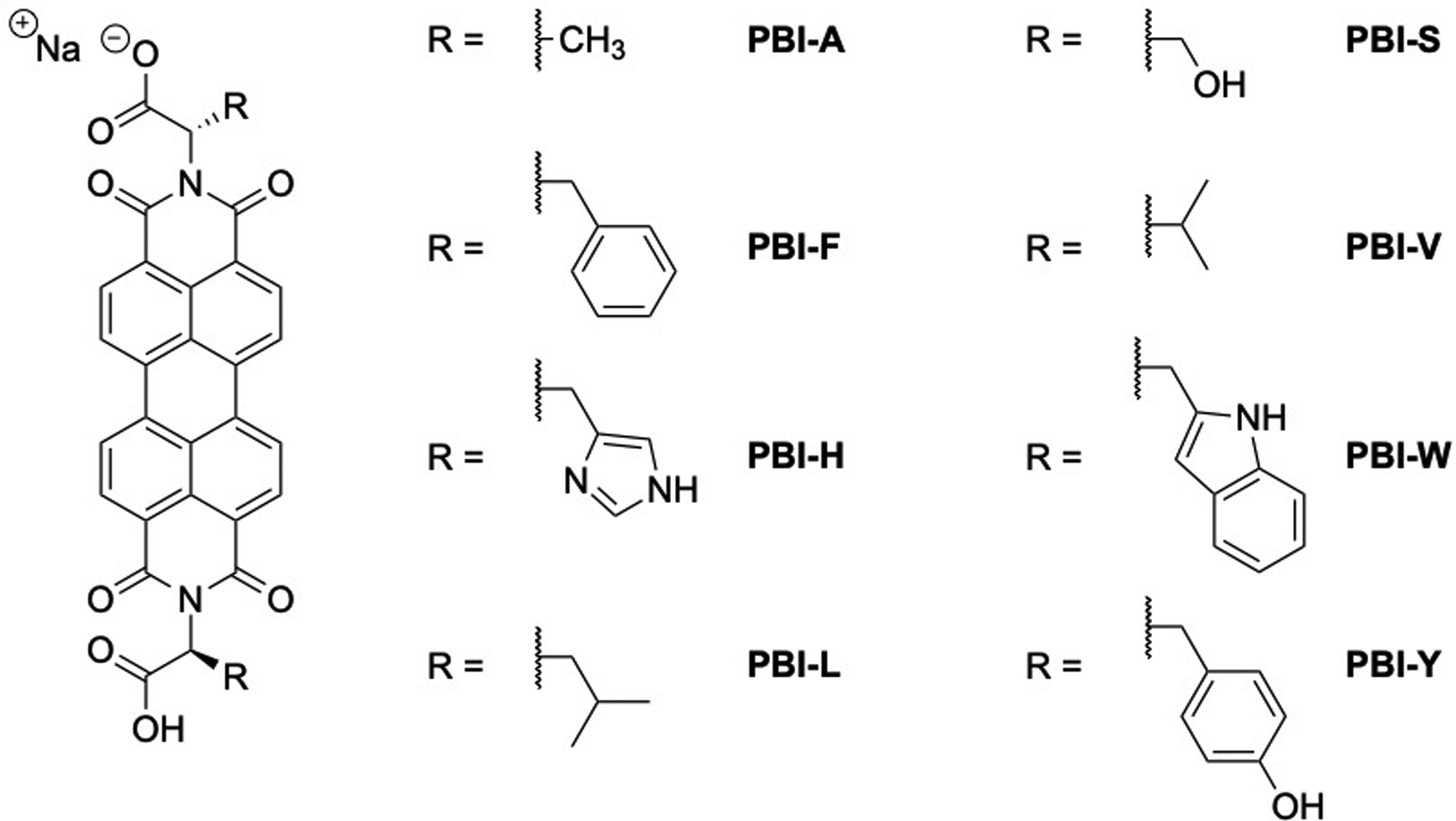 | ||
| Fig. 1 Structures of PBI materials studied as electron transporting interlayers. | ||
Experimental
PBIs were synthesised as previously reported.24,27 In general, 1 equivalent perylenetetracarboxylic dianhydride, 2 equivalents of the amino acid and 40 equivalents of imidazole were added to a flask which was purged with nitrogen. The reaction mixture was heated at 120 °C for 5 hours before being cooled to 90 °C. Deionised H2O was then added, and the reaction was left for a further 1 hour before being cooled to room temperature. Unreacted perylenetetracarboxylic dianhydride was then filtered off and the filtrate was acidified to a pH 2–3 using 2 M HCl(aq) solution. This caused the amino acid appended PBI to precipitate and this was filtered before being dried in a vacuum oven overnight with a further freeze-drying step to remove any water.PBI solutions were prepared at a concentration of 5 mg mL−1 by the addition of 1 equivalent of a 0.1 M NaOH solution and then made to concentration with distilled water. These solutions were then left to stir overnight to ensure dissolution of the material. Regioregular P3HT was purchased from Sigma-Aldrich (product number 445703), and PC61BM (>99.5%) was purchased from Ossila.
Indium-doped tin oxide (ITO) covered glass slides KINTEC, (7 Ω sq−1, 15 mm × 15 mm × 1.1 mm) were cleaned by submerging in deionised water, acetone and isopropanol respectively, with ultrasonication for 5 minutes in each solvent. The substrates were then dried over a stream of compressed air before being treated with O2 plasma (Diener Electronic, Zepto model) for 10 minutes. Zinc oxide precursor solution29 was spin-coated at 2000 rpm for 60 seconds with a ramp of 10 seconds, in ambient, at room temperature and annealed at 120 °C for 30 seconds in air. The PBI solution was then spin-coated on top of the ZnO layer by spinning at 2000 rpm for 60 seconds, with a ramp of 10 seconds, in the ambient, at room temperature. The substrates were then annealed at 120 °C for 20 minutes in air. A P3HT/PC61BM solution (36 mg mL−1 total concentration, 1![[thin space (1/6-em)]](https://www.rsc.org/images/entities/char_2009.gif) :0.8 ratio, in chlorobenzene) had been stirred overnight at 40 °C in a nitrogen-filled glovebox. The active layer was deposited at 1000 rpm for 60 seconds with a ramp of 10 seconds, in a nitrogen atmosphere at room temperature and the films were annealed at 150 °C for 20 minutes in a nitrogen atmosphere. Molybdenum trioxide (10 nm) was then deposited by thermal evaporation (∼10−5 mbar) before deposition of silver electrodes (100 nm) by thermal evaporation (∼10−5 mbar) using a shadow mask (electrode dimensions 1.5 mm × 3.5 mm).
:0.8 ratio, in chlorobenzene) had been stirred overnight at 40 °C in a nitrogen-filled glovebox. The active layer was deposited at 1000 rpm for 60 seconds with a ramp of 10 seconds, in a nitrogen atmosphere at room temperature and the films were annealed at 150 °C for 20 minutes in a nitrogen atmosphere. Molybdenum trioxide (10 nm) was then deposited by thermal evaporation (∼10−5 mbar) before deposition of silver electrodes (100 nm) by thermal evaporation (∼10−5 mbar) using a shadow mask (electrode dimensions 1.5 mm × 3.5 mm).
Transmittance measurements were carried out using ZnO/PBI bilayer films deposited on ITO as described for the OPV fabrication. The spectra were recorded using a Shimadzu UV 2700 instrument.
The current–voltage characterisation of the fabricated devices was carried out using a Keithley 4200-SCS and a Newport solar simulator with a 150 W xenon arc lamp was used for AM1.5 illumination, which was confirmed using a calibrated solar cell. All tests were carried out in a nitrogen-filled glovebox. The J–V characteristics of a minimum of 14 devices was used to calculate the average performance. External quantum efficiency measurements were carried out using a Gooch and Housego OL 750 automated spectroradiometric measurement system, with a calibrated silicon detector (OL-750-HSD-300).
Atomic force microscopy (AFM) was carried using an Innova AFM from Bruker. The surface topographies were probed using tapping mode. Film thickness was measured by slitting the films using a sharp blade to measure the height profile. The average thickness was calculated from 10 traces.
Results and discussion
There are many physical properties that can influence the performance of materials as electron transporting layers in OPVs. The amino acid functionalised PBIs self-assemble in water at high pH and therefore the small changes in molecular structure can result in significant changes to the absorption, electrochemical properties or photoconductivity for example,24 all of which can influence OPV performance.The transmittance of PBI layers deposited on ITO/ZnO was studied in order to compare the effect of different side chains (Fig. 2). P3HT/PC61BM films have a broad absorption peak between 400–700 nm,30 which overlaps with PBI absorption. If the PBI layer is too strongly absorbing, it could reduce the number of charge carriers formed in the active layer. PBI-L is the strongest absorbing layer by far, with a transmittance of just 15.2% at the wavelength of maximum absorbance (λmax), due to its larger thickness with respect to the other materials (Table S1, ESI†). PBI-H is the next strongest absorbing material with a transmittance of 53.8% at 509 nm and also forms the second thickest film from the series. PBI-A has the highest transmission at 72.3% in the visible region, whilst PBI-Y is slightly lower at 69.5%. These two double layers (on ZnO) are thin with measured thicknesses of 38 and 39 nm, respectively (Table S1, ESI†). The other double layers (containing PBI-F, PBI-S, PBI-V or PBI-W) have similar transmittances between 58.5–63.1%. The absorbance range for the materials could be influenced by different types of aggregation promoted by the side chains.
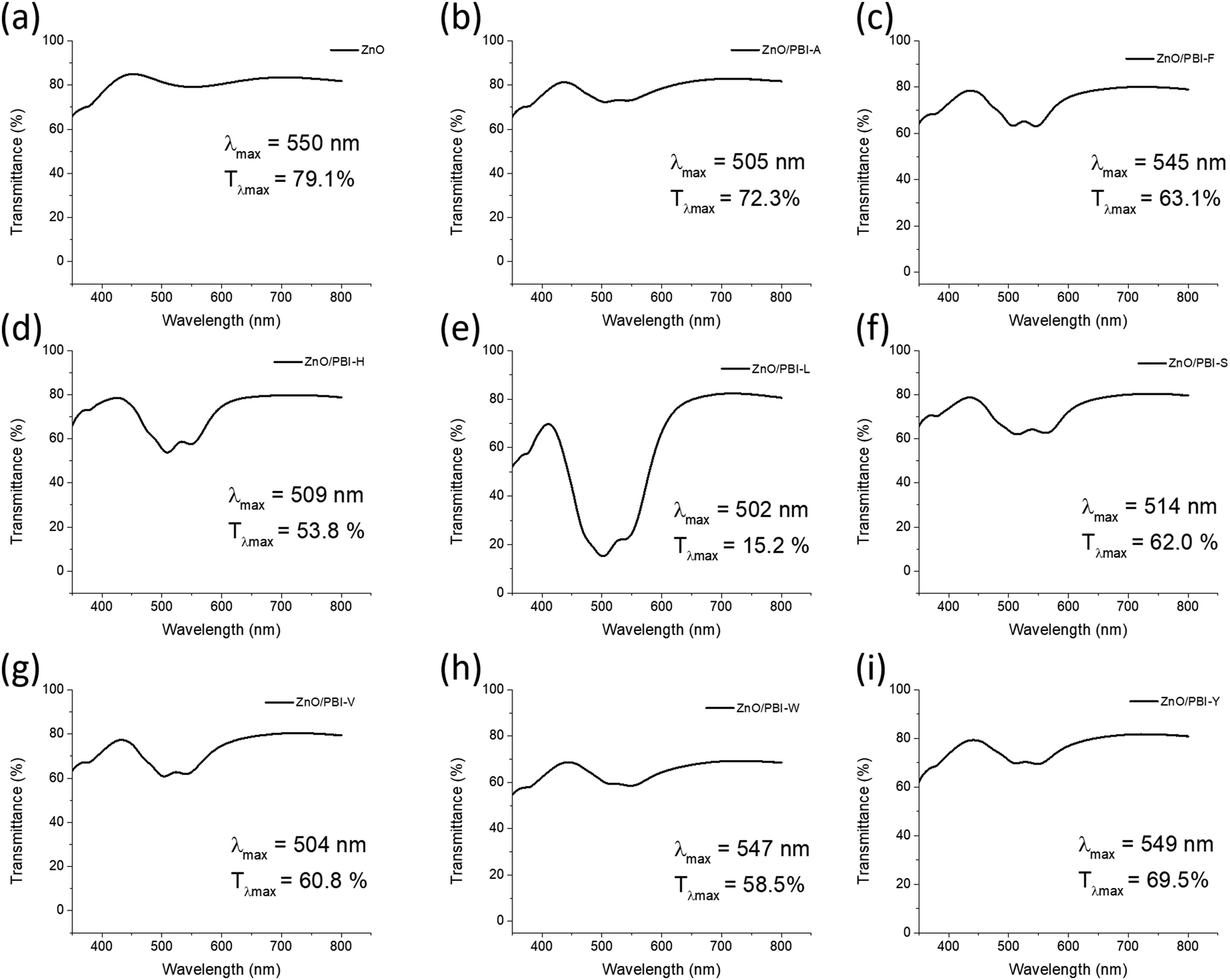 | ||
| Fig. 2 Transmittance spectra of (a) ITO/ZnO and ITO/ZnO/PBI films where the PBI material used is (b) PBI-A (38 nm), (c) PBI-F (26 nm), (d) PBI-H (71 nm), (e) PBI-L (264 nm), (f) PBI-S (38 nm), (g) PBI-V (37 nm), (h) PBI-W (66 nm), (i) PBI-Y (39 nm). Transmittance at λmax is reported for the visible region. The average thickness measured for the ZnO/PBI double layers are stated in parentheses. | ||
It is important to ensure that the electron affinity and ionisation energy are suitably matched to avoid introducing energy barriers between layers. In inverted solar cells the interlayer will be used to facilitate charge transport from PC61BM to ZnO. The work function of zinc oxide is 4.1 eV29 and although reported values for the electron affinity range from 3.62–4.38 eV31 due to differences in reporting cyclic voltammetry data, Guan et al. reported an electron affinity for a spin-coated PC61BM film of 3.8 eV using inverse photoemission spectroscopy.32
The previously reported electron affinities of the PBI materials studied are listed in Table S2 (ESI†).24 These energy levels lie between the ZnO and PC61BM or approximately level with ZnO, which suggests the inclusion of the PBI interlayer should not create any energy barriers and can assist with charge transport in the OPV devices. The ionisation energies are also far from the reported value for regioregular P3HT of ∼4.5–4.7 eV,33–36 therefore preventing transport of holes which could lead to recombination.
The PBI layers were applied as interlayers between the zinc oxide electron transport layer and the P3HT/PC61BM active layer with the results summarised in Table 1 and example J–V plots presented in Fig. S1 (ESI†). P3HT/PC61BM based solar cells were selected for these experiments as they are well studied and therefore make suitable reference devices. The reported efficiency of inverted OPVs containing a P3HT/PC61BM active layer can vary between 1.9–3.85%37–40 depending on variables such as the polymer batch and the conditions used for processing. Previous examples of P3HT/PC61BM devices with a PBI-related electron transport layer include a report by Nian and co-workers that showed a large increase in PCE to 4.48% when the PBI material (also named PBI-H, see Fig. 3) was used as a cathode interlayer by depositing from THF solutions, with the ZnO reference giving a PCE of 3.13%.41 Also, the use of the material PDIN-H (Fig. 3), by Harding et al. showed a 2.7% PCE, compared to 2.8% for the ZnO control device.23 This example is comparable to the best performing amino acid appended PBIs which exhibit higher JSC values, but lower VOC and fill factors, which may be attributed to differences in fabrication methods and the P3HT used.
| ETL | V OC (V) | Fill factor | J SC (mA cm−2) | PCEb (%) |
|---|---|---|---|---|
| a J SC calculated from the integration of EQE plots shown in parentheses. b Standard deviation presented in parentheses. | ||||
| ZnO (reference) | 0.58 | 0.50 | 7.78 (7.54) | 2.25 (0.44) |
| ZnO/PBI-A | 0.36 | 0.45 | 6.14 (6.52) | 1.00 (0.24) |
| ZnO/PBI-F | 0.58 | 0.49 | 8.87 (10.18) | 2.55 (0.16) |
| ZnO/PBI-H | 0.53 | 0.47 | 7.06 (7.67) | 1.96 (0.33) |
| ZnO/PBI-L | 0.54 | 0.36 | 3.56 (4.06) | 0.72 (0.19) |
| ZnO/PBI-S | 0.55 | 0.50 | 7.39 (7.21) | 2.03 (0.28) |
| ZnO/PBI-V | 0.51 | 0.47 | 6.75 (7.55) | 1.64 (0.43) |
| ZnO/PBI-W | 0.61 | 0.50 | 7.38 (7.30) | 2.24 (0.26) |
| ZnO/PBI-Y | 0.61 | 0.48 | 7.64 (6.25) | 2.21 (0.22) |
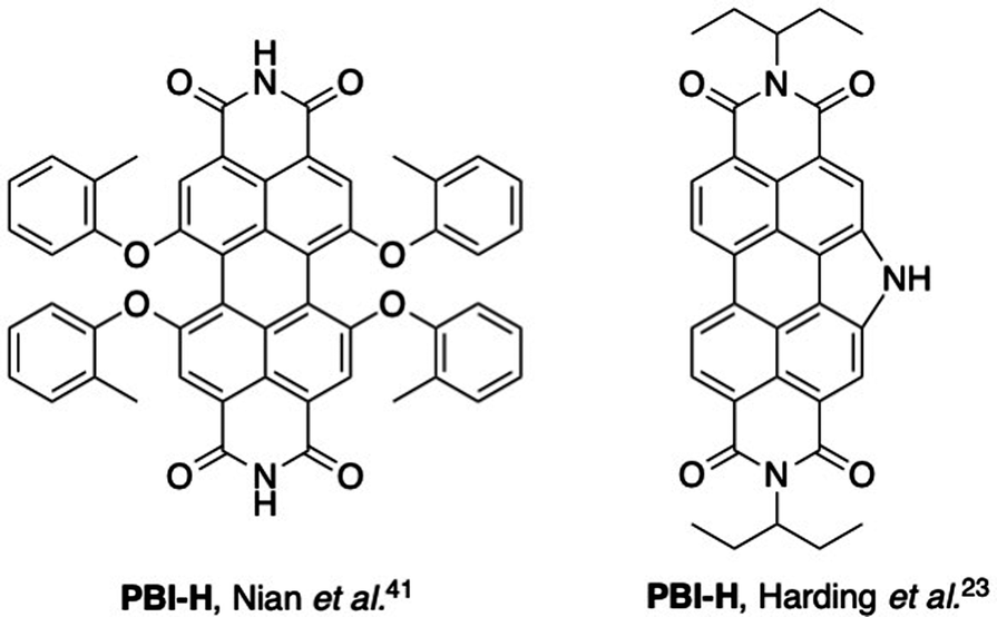 | ||
| Fig. 3 Structures of PBI-based materials previously used as electron transporting interlayers in P3HT/PC61BM OPVs.23,41 | ||
Using PBI-F as the interlayer results in an increase in the short circuit current density (JSC) with respect to the reference device containing only a zinc oxide layer. This results in an average PCE of 2.55% which is higher than for the reference device (PCE = 2.25%). Although adding a PBI interlayer may reduce the amount of light reaching the active layer, the electron deficient nature of PBIs can assist with charge separation of the exciton, resulting in improved short-circuit current. Layers PBI-W and PBI-Y show a slight reduction in the short-circuit current density compared to the reference but an increased open-circuit voltage (VOC) results in similar PCEs for these devices (2.24% and 2.21%, respectively).
Devices containing PBI-L exhibit the lowest JSC and PCE and this can be explained by the parasitic absorption of the PBI-L layer, which has an approximate three-fold reduction in transmittance at the λmax compared to the other PBI layers. Similarly, PBI-H had the second strongest absorption of the films and has a low JSC and consequently PCE, attributed to parasitic absorption from the interlayer.
External quantum efficiency (EQE) plots for the fabricated devices are shown in Fig. S2 (ESI†). The solar cell containing only a ZnO electron transport layer had a peak EQE of 34.9% at 547 nm. All devices containing PBI layers showed reduced EQE at the same wavelength, highlighting the parasitic absorption from the strongly absorbing PBI layers, particularly in PBI-L. However, there is increased absorption at lower wavelengths in the best performing PBI-containing devices. This is most evident in cells containing PBI-F which has an EQE of 35.7% at 450 nm, which is significantly larger than the ZnO-based device with an EQE of 24.3% at the same wavelength. This suggests that there is improved absorption of the P3HT/PC61BM layer where there is no parasitic absorption from the PBI and this suggests that some of the PBI interlayers improve charge transport in the photovoltaic devices. Cells containing PBI-A, PBI-F, PBI-H, PBI-S and PBI-W have a larger EQE at 450 nm compared to the reference ZnO-based device. Clearly, there is a difficult balance to be struck in using PBI electron transporting interlayers where an improvement in charge transport can be counteracted by a reduction in the number of charge carriers due to absorption of the PBI layer.
Although PBI-A shows low transmittance and low electron affinity, the OPV performance when this layer is used is low, with an especially large reduction in the VOC. This can be explained by atomic force microscopy studies. Images of P3HT/PC61BM deposited layers onto PBI-A, PBI-F and ZnO surfaces have been presented in Fig. 4. All images show common features of the long narrow ZnO aggregates. However, the topography image of the active layer on PBI-A shows many small domains suggesting that there is phase segregation, whilst the bulk films of the active layers deposited on PBI-F and ZnO are mostly uniform. Tang and co-workers previously showed that the large donor/acceptor areas caused by phase segregation can lead to non-radiative recombination and a loss of voltage in the solar cells,42 which is consistent with the observations for PBI-A based devices.
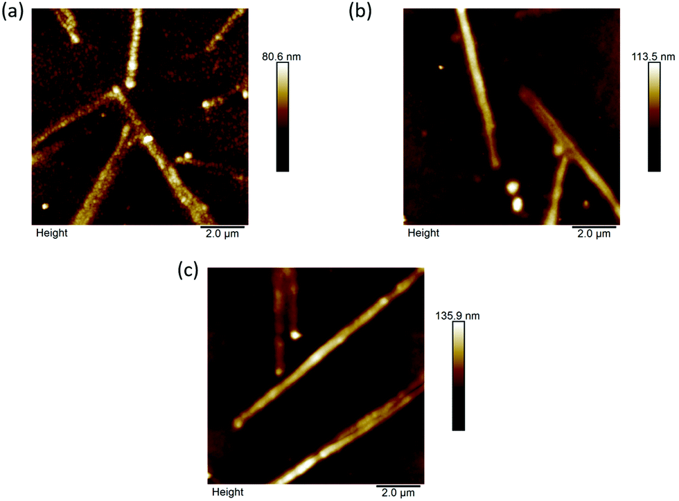 | ||
| Fig. 4 AFM topography images of P3HT/PC61BM deposited on (a) ITO/ZnO/PBI-A, (b) ITO/ZnO/PBI-F and (c) ITO/ZnO. | ||
There is a general trend where the best performing PBI layers (PBI-F, PBI-W and PBI-Y) are also those that exhibit a λmax at ∼545 nm, which is ascribed to the S0–S1 transition, whereas other materials show a λmax at ∼505 nm for the S0–S2 transition. The absorption profile in thin film is influenced by the molecular packing.24 Therefore, we believe that improved molecular packing in PBI-F, PBI-W and PBI-Y is responsible for their improved performance compared to the other amino acid-appended PBI materials. In addition to an overall improvement in efficiency, the open-circuit voltage values are highest when these three materials are used as interlayers. The open-circuit voltage is affected by many factors including morphology, work function of electrodes and the HOMO energy of the donor and LUMO energy of the acceptor for example.43 As all of these PBI materials have similar energy levels (Table S2, ESI†), it is most likely that the aggregation of the PBIs, leading to improved electron extraction, will have the largest influence on the difference in VOC in the series of compounds. The higher VOC values for PBI-F, PBI-W and PBI-Y provides further evidence that these aggregate more favourably for electron transport. It is noted that these materials contain the largest aromatic side groups of the PBI materials, therefore we expect that π–π stacking plays an important role in inducing more favourable aggregation.
The photoconductivity of the interlayer can also have an influence on the device performance. Zhao et al. showed that an asymmetric PBI enhanced the photoconductivity when used to dope the ZnO layer and this contributed to increased efficiency of PTB7/PC71BM based OPVs.44 When the photoconductivity of the amino acid appended PBIs was studied, PBI-F, PBI-Y and PBI-W showed the lowest photoconductivity, indicating that radical anions (or dianions) were not readily formed under illumination.24 Notably, it is these materials that are used in the highest performing OPV devices, and indeed exhibit the highest open-circuit voltages. This suggests that formation of PBI radical anions or dianions in the interlayer upon illumination (in additions to free charge carriers formed in the bulk heterojunction after charge transfer) can lead to recombination and thus reduce the efficiency of the OPVs. The trend does not hold for the whole series, i.e., the most photoconductive material does not give the worst performance as an interlayer. However, this can be partially explained by other factors, such as the PBI-L layer showing the strongest parasitic absorption for example. This highlights the importance of molecular design for PBI materials to be used in solar cells as subtle changes to the molecular structure can have large implications for device performance.
Conclusions
A series of amino acid appended PBIs have been used as interlayers between ZnO and P3HT/PC61BM in inverted OPV devices with the phenylalanine (PBI-F) derivative in particular showing good short-circuit current, whilst tryptophan (PBI-W) and tyrosine (PBI-Y) analogues improve the open-circuit voltage with only a small reduction in short-circuit current. The PBIs are deposited from basic aqueous solutions, highlighting that these materials show promising performance for solution-processed multilayer devices where orthogonal processing is necessary. Moreover, the use of aqueous solutions allows for ‘greener’ processing, which is an important consideration for the manufacturing of organic photovoltaics, particularly as they have the potential to be fabricated on a large scale. Further development of such materials could be promising for implementation in tandem solar cells which can be a successful strategy for enhancing the power conversion efficiency of organic photovoltaics.Conflicts of interest
There are no conflicts to declare.Acknowledgements
The authors thank EPSRC for funding (EP/L021978/2, EP/P02744X/2, EP/S032673/1). E. R. D. thanks the Leverhulme Trust for funding (ECF-2017-223) and the University of Glasgow for an LKAS Leadership Fellowship. Raw data associated with the manuscript can be accessed at http://dx.doi.org/10.5525/gla.researchdata.1186.References
- X. Chang, J. Fang, Y. Fan, T. Luo, H. Su, Y. Zhang, J. Lu, L. Tsetseris, T. D. Anthopoulos, S. Liu and K. Zhao, Adv. Mater., 2020, 32, 2001243 CrossRef CAS PubMed.
- D.-Y. Son, J.-W. Lee, Y. J. Choi, I.-H. Jang, S. Lee, P. J. Yoo, H. Shin, N. Ahn, M. Choi, D. Kim and N.-G. Park, Nat. Energy, 2016, 1, 16081 CrossRef CAS.
- R. Zhou, Z. Jiang, C. Yang, J. Yu, J. Feng, M. A. Adil, D. Deng, W. Zou, J. Zhang, K. Lu, W. Ma, F. Gao and Z. Wei, Nat. Commun., 2019, 10, 5393 CrossRef PubMed.
- M.-A. Pan, T.-K. Lau, Y. Tang, Y.-C. Wu, T. Liu, K. Li, M.-C. Chen, X. Lu, W. Ma and C. Zhan, J. Mater. Chem. A, 2019, 7, 20713–20722 RSC.
- X. Liu, X. Li, N. Zheng, C. Gu, L. Wang, J. Fang and C. Yang, ACS Appl. Mater. Interfaces, 2019, 11, 43433–43440 CrossRef CAS PubMed.
- Z.-G. Zhang, Y. Yang, J. Yao, L. Xue, S. Chen, X. Li, W. Morrison, C. Yang and Y. Li, Angew. Chem., Int. Ed., 2017, 56, 13503–13507 CrossRef CAS PubMed.
- Y. Cai, Y. Li, R. Wang, H. Wu, Z. Chen, J. Zhang, Z. Ma, X. Hao, Y. Zhao, C. Zhang, F. Huang and Y. Sun, Adv. Mater., 2021, 33, 2101733 CrossRef CAS PubMed.
- Y. Lin, A. Magomedov, Y. Firdaus, D. Kaltsas, A. El-Labban, H. Faber, D. R. Naphade, E. Yengel, X. Zheng, E. Yarali, N. Chaturvedi, K. Loganathan, D. Gkeka, S. H. AlShammari, O. M. Bakr, F. Laquai, L. Tsetseris, V. Getautis and T. D. Anthopoulos, ChemSusChem, 2021, 14, 3569–3578 CrossRef CAS PubMed.
- Q. Liu, Y. Jiang, K. Jin, J. Qin, J. Xu, W. Li, J. Xiong, J. Liu, Z. Xiao, K. Sun, S. Yang, X. Zhang and L. Ding, Sci. Bull., 2020, 65, 272–275 CrossRef CAS.
- Y. Cui, Y. Xu, H. Yao, P. Bi, L. Hong, J. Zhang, Y. Zu, T. Zhang, J. Qin, J. Ren, Z. Chen, C. He, X. Hao, Z. Wei and J. Hou, Adv. Mater., 2021, 33, 2102420 CrossRef CAS PubMed.
- J. Wang, Z. Zheng, Y. Zu, Y. Wang, X. Liu, S. Zhang, M. Zhang and J. Hou, Adv. Mater., 2021, 33, 2102787 CrossRef CAS PubMed.
- Y. Zhou, C. Fuentes-Hernandez, J. Shim, J. Meyer, A. J. Giordano, H. Li, P. Winget, T. Papadopoulos, H. Cheun, J. Kim, M. Fenoll, A. Dindar, W. Haske, E. Najafabadi, T. M. Khan, H. Sojoudi, S. Barlow, S. Graham, J.-L. Brédas, S. R. Marder, A. Kahn and B. Kippelen, Science, 2012, 336, 327–332 CrossRef CAS PubMed.
- J. Subbiah, V. D. Mitchell, N. K. C. Hui, D. J. Jones and W. W. H. Wong, Angew. Chem., Int. Ed., 2017, 56, 8431–8434 CrossRef CAS PubMed.
- Y.-M. Chang and C.-Y. Leu, J. Mater. Chem. A, 2013, 1, 6446–6451 RSC.
- Y. Liu, C. Mu, K. Jiang, J. Zhao, Y. Li, L. Zhang, Z. Li, J. Y. L. Lai, H. Hu, T. Ma, R. Hu, D. Yu, X. Huang, B. Z. Tang and H. Yan, Adv. Mater., 2015, 27, 1015–1020 CrossRef CAS PubMed.
- D. Meng, D. Sun, C. Zhong, T. Liu, B. Fan, L. Huo, Y. Li, W. Jiang, H. Choi, T. Kim, J. Y. Kim, Y. Sun, Z. Wang and A. J. Heeger, J. Am. Chem. Soc., 2016, 138, 375–380 CrossRef CAS PubMed.
- Z. Luo, T. Liu, W. Cheng, K. Wu, D. Xie, L. Huo, Y. Sun and C. Yang, J. Mater. Chem. C, 2018, 6, 1136–1142 RSC.
- K. Jiang, F. Wu, H. Yu, Y. Yao, G. Zhang, L. Zhu and H. Yan, J. Mater. Chem. A, 2018, 6, 16868–16873 RSC.
- X. Wen, A. Nowak-Król, O. Nagler, F. Kraus, N. Zhu, N. Zheng, M. Müller, D. Schmidt, Z. Xie and F. Würthner, Angew. Chem., Int. Ed., 2019, 58, 13051–13055 CrossRef CAS PubMed.
- D. Hu, L. Yao, B. Yang and Y. Ma, Philos. Trans. R. Soc., A, 2015, 373, 20140318 CrossRef PubMed.
- Z.-G. Zhang, B. Qi, Z. Jin, D. Chi, Z. Qi, Y. Li and J. Wang, Energy Environ. Sci., 2014, 7, 1966–1973 RSC.
- Z. Wang, N. Zheng, W. Zhang, H. Yan, Z. Xie, Y. Ma, F. Huang and Y. Cao, Adv. Energy Mater., 2017, 7, 1700232 CrossRef.
- C. R. Harding, J. Cann, A. Laventure, M. Sadeghianlemraski, M. Abd-Ellah, K. R. Rao, B. S. Gelfand, H. Aziz, L. Kaake, C. Risko and G. C. Welch, Mater. Horiz., 2020, 7, 2959–2969 RSC.
- E. R. Draper, L. J. Archibald, M. C. Nolan, R. Schweins, M. A. Zwijnenburg, S. Sproules and D. J. Adams, Chem. – Eur. J., 2018, 24, 4006–4010 CrossRef CAS PubMed.
- V. Adams, J. Cameron, M. Wallace and E. R. Draper, Chem. – Eur. J., 2020, 26, 9879–9882 CrossRef CAS PubMed.
- S. Roy, D. Kumar Maiti, S. Panigrahi, D. Basak and A. Banerjee, RSC Adv., 2012, 2, 11053–11060 RSC.
- E. R. Draper, J. J. Walsh, T. O. McDonald, M. A. Zwijnenburg, P. J. Cameron, A. J. Cowan and D. J. Adams, J. Mater. Chem. C, 2014, 2, 5570–5575 RSC.
- E. R. Draper, J. R. Lee, M. Wallace, F. Jäckel, A. J. Cowan and D. J. Adams, Chem. Sci., 2016, 7, 6499–6505 RSC.
- S. Höfle, A. Schienle, M. Bruns, U. Lemmer and A. Colsmann, Adv. Mater., 2014, 26, 2750–2754 CrossRef PubMed.
- F. Zheng, X.-Y. Yang, P.-Q. Bi, M.-S. Niu, C.-K. Lv, L. Feng, W. Qin, Y.-Z. Wang, X.-T. Hao and K. P. Ghiggino, Org. Electron., 2017, 44, 149–158 CrossRef CAS.
- B. W. Larson, J. B. Whitaker, X.-B. Wang, A. A. Popov, G. Rumbles, N. Kopidakis, S. H. Strauss and O. V. Boltalina, J. Phys. Chem. C, 2013, 117, 14958–14964 CrossRef CAS.
- Z.-L. Guan, J. B. Kim, H. Wang, C. Jaye, D. A. Fischer, Y.-L. Loo and A. Kahn, Org. Electron., 2010, 11, 1779–1785 CrossRef CAS.
- H. Aarnio, P. Sehati, S. Braun, M. Nyman, M. P. de Jong, M. Fahlman and R. Österbacka, Adv. Energy Mater., 2011, 1, 792–797 CrossRef CAS.
- N. Chandrasekaran, A. Kumar, L. Thomsen, D. Kabra and C. R. McNeill, Mater. Adv., 2021, 2, 2045–2054 RSC.
- R. J. Davis, M. T. Lloyd, S. R. Ferreira, M. J. Bruzek, S. E. Watkins, L. Lindell, P. Sehati, M. Fahlman, J. E. Anthony and J. W. P. Hsu, J. Mater. Chem., 2011, 21, 1721–1729 RSC.
- J.-P. Sun, J. T. Blaskovits, T. Bura, S. Beaupré, M. Leclerc and I. G. Hill, Org. Electron., 2017, 50, 115–120 CrossRef CAS.
- K. D. M. Rao, C. Hunger, R. Gupta, G. U. Kulkarni and M. Thelakkat, Phys. Chem. Chem. Phys., 2014, 16, 15107–15110 RSC.
- N. Chander, S. Singh and S. S. K. Iyer, Sol. Energy Mater. Sol. Cells, 2017, 161, 407–415 CrossRef CAS.
- L. Yan, J. Yi, Q. Chen, J. Dou, Y. Yang, X. Liu, L. Chen and C.-Q. Ma, J. Mater. Chem. A, 2017, 5, 10010–10020 RSC.
- L. K. Jagadamma, M. Abdelsamie, A. El Labban, E. Aresu, G. O. Ngongang Ndjawa, D. H. Anjum, D. Cha, P. M. Beaujuge and A. Amassian, J. Mater. Chem. A, 2014, 2, 13321–13331 RSC.
- L. Nian, W. Zhang, S. Wu, L. Qin, L. Liu, Z. Xie, H. Wu and Y. Ma, ACS Appl. Mater. Interfaces, 2015, 7, 25821–25827 CrossRef CAS PubMed.
- Z. Tang, J. Wang, A. Melianas, Y. Wu, R. Kroon, W. Li, W. Ma, M. R. Andersson, Z. Ma, W. Cai, W. Tress and O. Inganäs, J. Mater. Chem. A, 2018, 6, 12574–12581 RSC.
- N. K. Elumalai and A. Uddin, Energy Environ. Sci., 2016, 9, 391–410 RSC.
- H. Zhao, Y. Luo, L. Liu, Z. Xie and Y. Ma, Mater. Chem. Front., 2017, 1, 1087–1092 RSC.
Footnote |
| † Electronic supplementary information (ESI) available. See DOI: 10.1039/d1tc04622e |
| This journal is © The Royal Society of Chemistry 2022 |