
 Open Access Article
 This Open Access Article is licensed under a
 Creative Commons Attribution 3.0 Unported Licence
Defect formation and healing at grain boundaries in lead-halide perovskites†
Waldemar
Kaiser
 *a,
Kashif
Hussain
bc,
Ajay
Singh
d,
Asma A.
Alothman
e,
Daniele
Meggiolaro
a,
Alessio
Gagliardi
b,
Edoardo
Mosconi
*ae and
Filippo
De Angelis
af
*a,
Kashif
Hussain
bc,
Ajay
Singh
d,
Asma A.
Alothman
e,
Daniele
Meggiolaro
a,
Alessio
Gagliardi
b,
Edoardo
Mosconi
*ae and
Filippo
De Angelis
af
aComputational Laboratory for Hybrid/Organic Photovoltaics (CLHYO), Istituto CNR di Scienze e Tecnologie Chimiche “Giulio Natta” (CNR-SCITEC), Via Elce di Sotto 8, Perugia 06123, Italy. E-mail: waldemar.kaiser@scitec.cnr.it; edoardo.mosconi@cnr.it
bDepartment of Electrical and Computer Engineering, Technical University of Munich, Hans-Piloty-Straße 1, 85748 Garching, Germany
cDepartment of Electrical Engineering, Sukkur IBA University, Sukkur 65200, Pakistan
dDepartment of Physics and Materials Science, University of Luxembourg, Luxembourg L-1511, Luxembourg
eDepartment of Chemistry, College of Science, King Saud University, P.O. Box 22452, Riyadh 11495, Kingdom of Saudi Arabia
fDepartment of Chemistry, Biology and Biotechnology, University of Perugia and UdR INSTM, Via Elce di Sotto 8, Perugia 06123, Italy
First published on 11th November 2022
Abstract
Polycrystalline perovskite solar cells show high power conversion efficiencies despite the presence of grain boundaries (GBs). The benign nature of GBs on the electronic properties and structural stability in metal-halide perovskites contradicts their propensity for point defect formation, a controversy that is far from being understood. In this work, we combine ab initio molecular dynamics and density functional theory calculations on the Σ5[130] GB of cesium lead iodide, CsPbI3, to shed light on the structural and electronic properties of such GBs. Our results present the first evidence of structural healing of GBs driven by the facile migration of iodine ions, resulting in stabilized GB structures with reduced hole trap states and shallow electron trap states by strain-induced Pb–Pb dimers. Drift-diffusion simulations reveal that shallow electron trap states in GB mainly lower open-circuit voltage by enhanced non-radiative recombination. Finally, we observe the spontaneous formation of iodine Frenkel defects with reduced formation energies compared to the perovskite bulk. Overall, our study reveals a controversy of GBs showing a moderate impact on the electronic properties by structural healing but a detrimental impact on the point defect densities, both being connected to the facile migration of iodine ions in GBs.
1. Introduction
Metal-halide perovskites (MHPs) have attracted extraordinary interest for next-generation photovoltaic technologies due to their favorable optoelectronic properties.1–3 Successive material and process engineering raised the power conversion efficiency to >25% in single-junction perovskite solar cells (PSCs)4 and 29.15% in perovskite–silicon tandem solar cells5 within only one decade. This success story is, however, quite surprising as the mechanically soft lattice in MHPs induces a lively and diverse defect chemistry,6,7 and MHP synthesis by low-temperature solution techniques may result in the coexistence of different phases8,9 and incomplete crystallization.10,11 Weak metal-halide bonds may further accelerate thermal and photochemical degradation of MHPs12–14 and support the formation of ionic point defects which may promote non-radiative recombination losses.15 In contrast, recent studies connected the high defect tolerance to the soft lattice, allowing carriers to couple only to low-frequency vibrations.16,17PSCs are typically made of polycrystalline MHP thin films containing nano-to micrometer-sized grains, separated by spatially extended grain boundaries (GBs), which strongly affect the device performance.18,19 Correa-Baena et al. observed an increased J–V hysteresis in thin film PSCs of small grain sizes, which has been attributed to reduced ion migration.20 In contrast, conductive atomic force microscopy discovered enhanced iodine migration in high-angle GBs.21 Ionic point defects, particularly iodine interstitials and vacancies, can easily migrate within the MHP crystal lattice.22,23 At the same time, GBs may trap iodine point defects and suppress ion migration from the GB to the grain interior.24,25 Defects predominantly form on the grain surface, suggesting an enhanced defect density in polycrystalline MHP films with respect to single crystals.26 Photoemission spectroscopy studies revealed the presence of defect clusters at GBs with energy levels close to the valence band maximum (VBM) and significant cross-section for hole trapping.27 Photoluminescence (PL) measurements showed substantial variations in PL intensities and lifetimes between different grains within the same MPH thin film.28,29 The origin of such grain to grain variations is attributed to variations in the crystallographic misalignment and the accompanying local strain at GBs, potentially enhancing trap densities.30 GBs may further accelerate irreversible degradation in oxygen31 and moisture,32 causing long-term instabilities. Consequently, GB passivation33,34 and strain engineering35 are promising strategies to mitigate non-radiative recombination losses and stabilize MHP thin films.
Point defects face significant structural differences within GBs and at surfaces compared to the bulk,36 which, however, is challenging to probe experimentally.37 First-principles atomistic simulations can provide relevant insight into the structural and electronic properties of MHP GBs.36 Meggiolaro et al.39 reported the favored formation of iodine interstitials, the most movable point defects in MHPs,22,38 at MHP surfaces due to reduced steric hindrance.39 Non-adiabatic molecular dynamics simulations40 revealed increased non-radiative recombination at the Σ5[012] GB (see ref. (36) for the explanation of the notation) of methylammonium lead iodide, MAPbI3. In contrast, the high-angle Σ5[310] GB may suppress charge recombination by spatially separating the electron from the hole.41 Density functional theory (DFT) studies showed the lack of deep electronic states in the band gap for a variety of MHP GBs, while only shallow states near the VBM are reported, which potentially hamper hole transport across the GB.42 Point defects, in particular lead interstitials and IMA and IPb anti-site defects, introduce mid-gap electronic states in MAPbI3 GBs.43 Furthermore, at the Σ5[130] GB of cesium lead iodide, CsPbI3, iodine interstitials are stabilized at the GB and introduce gap states which may trap charge carriers and promote non-radiative charge recombination.44
Existing studies analyzed the structural and electronic properties of MHP GBs from ground state DFT calculations.42–44 Several dynamical properties of MHPs, however, are being attributed to the soft lattice, such as strong dynamical fluctuations, ionic migration, and anharmonicities in the octahedral tilting.8,9,45–47 Thus, it is of high interest to unravel the consequences of the soft nature of MHPs on such GBs. To shed light on the structural and electronic properties of GBs under finite temperatures, we performed ab initio molecular dynamics (AIMD) simulations and DFT calculations on the Σ5[130] GB of CsPbI3 as representative of lead-halide perovskites. Our AIMD simulations reveal a novel atomistic picture of the formation of defects and give unprecedented insight into the spontaneous healing of GB defects, which are directly connected to the facile migration of iodine ions inside GBs. AIMD and DFT further propose the presence of electron trap states inside the GB at finite temperatures, potentially enhancing non-radiative recombination losses. Finally, we report on the formation mechanism and energies of iodine Frenkel defects near lead–iodine rich GB regions, having strongly reduced defect formation energy at GB with respect to the MHP bulk region.
2. Model and computational details
We carried out Car–Parrinello molecular dynamics (CPMD)48–50 simulations with the Quantum Espresso package51 using the GGA-PBE52 exchange–correlation functional. Electron–ion interactions were described by scalar relativistic ultrasoft pseudopotentials with electrons from I 5s, 5p; Cs 5s, 5p, 6s; and Pb 6s, 6p, 5d shells explicitly included. Plane-wave basis set cutoffs for the smooth part of the wave functions and the augmented density were 25 and 200 Ry, respectively. The fictitious mass of the electronic degrees of freedom were set to 1000 au, and the atomic masses of all atoms to an identical value of 5 amu to enhance the dynamical sampling. An integration time step of 10 au was used. The atomic positions were randomized initially and then a thermostat was applied to maintain a temperature of 380 ± 30 K. DFT calculations of defect formation energies in the orthorhombic CsPbI3 bulk and the GB model were performed by geometry optimization of the ionic positions while keeping the supercell fixed, using with refined plane-wave basis set cutoffs of 40 and 320 Ry for the smooth part of the wave functions and the augmented density, respectively, using the PWscf module of the Quantum Espresso package.We have taken the atomic model of the CsPbI3 Σ5[130] GB, Fig. 1, from previous theoretical analysis42,44 which has a low formation energy EGB,form = 2.7 eV nm−2 (0.43 J m−2) with respect to the orthorhombic CsPbI3, being substantially lower than the ones of e.g. CdTe or Si GBs53,54 and comparable to low-energy GBs in Li-based solid-state electrolytes.55 The model contains two high-angle GBs made of a PbI- and a CsI-terminated region. The orthorhombic supercell is of size a = 12.695 Å, b = 19.242 Å, c = 76.972 Å. We first relaxed the ionic positions and then performed CPMD simulations on the optimized GB model as described above for ∼8.5 ps.
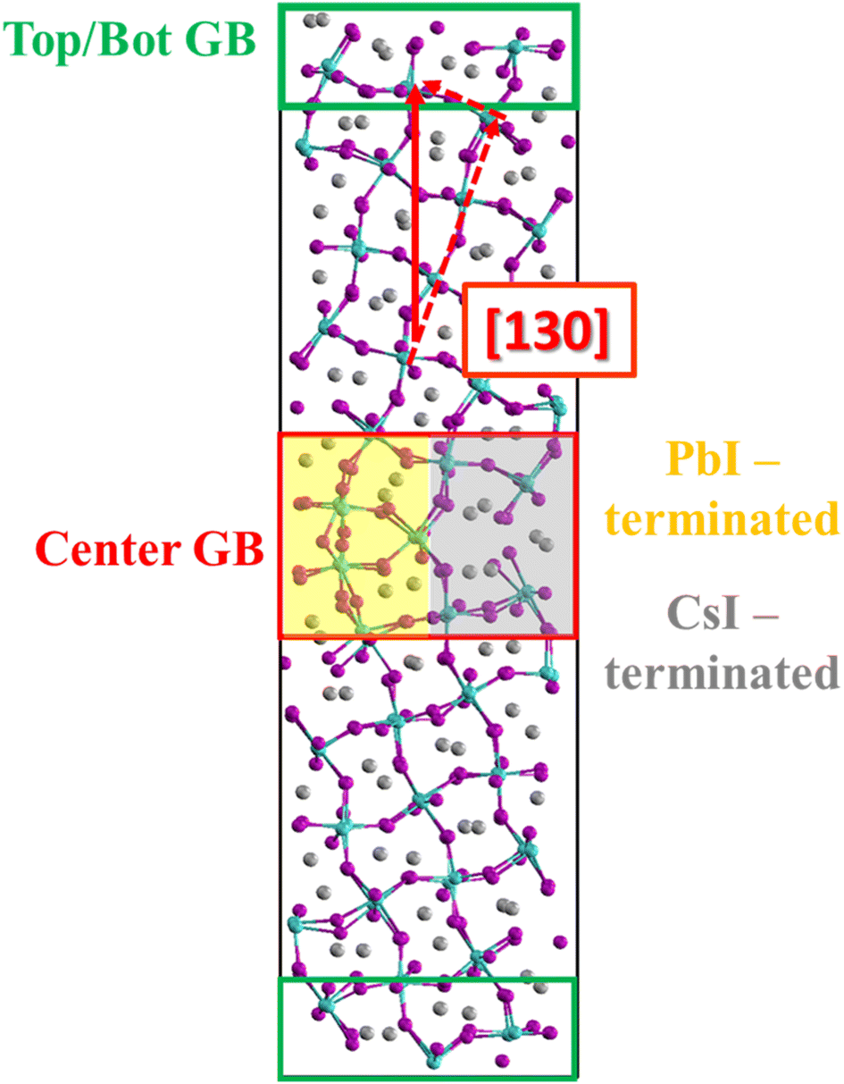 | ||
| Fig. 1 Structural model of the Σ5[130] GB of CsPbI3 with the center GB and top/bot GB highlighted in red and green, respectively. PbI-terminated and CsI-terminated regions in the center GB are indicated by the yellow and gray regions, respectively. | ||
Electronic structure calculations on several snapshots were performed using hybrid PBE0 exchange-correlation functional, keeping the fraction of Fock exchange α at its original value (0.25) in the freely available CP2K software package.56 Calculations have been carried out with Goedecker–Teter–Hutter pseudopotentials,57 double-ζ polarized basis sets for the wave functions (see Fig. S1, ESI,† for convergence test),58 and a cutoff of 300 Ry for the expansion of the electron density in plane waves. We used the auxiliary density matrix method with the cFIT auxiliary basis set to accelerate the hybrid functional calculations.59 As recently demonstrated,47 this setup further reproduces accurately structural and dynamical properties of MHPs.
3. Results and discussions
3.1 Structural evolution
We start our detailed analysis of the AIMD simulations by searching for the presence of typical iodine point defects within the GB supercell. Throughout the trajectory, we observe the appearance of split interstitials, i.e. two iodine ions shared between two lead centers, see inset in Fig. 2a and Section S2, ESI.† Most split interstitials are located in the GB regions, while signatures of bulk split interstitials are found between 6 and 8.5 ps of simulation time, Fig. 2a. The number of split interstitials in the top/bot GB increases within the first 3 ps and remains approximately constant at a value of 3 for the remainder of the trajectory, Fig. 2b. In the center GB, we see an increasing number of split interstitials from 1 at 0 ps to ∼4 at around 1 ps, which subsequently decreases to ∼1–2 after 2 ps of simulation time. After 6 ps, additional split interstitials arise within the center GB. The majority of split interstitials within the center GB are located in the PbI-terminated region, Fig. S2, ESI.† The formation and annihilation of split interstitials directly correlate with the amount of 90° Pb–I–Pb bond angles in the different regions, Fig. S3, ESI,† which is an indicator to reasonably distinguish amorphous, PbI2-rich from perovskite phases.60,61 We further highlight that split interstitials do not migrate from the GB into the bulk within the simulated timescales, confirming previous classical MD studies.62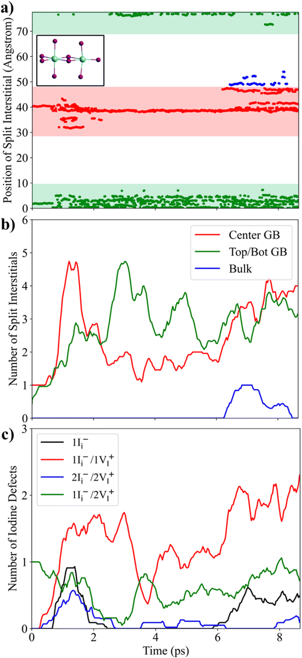 | ||
| Fig. 2 (a) Position of split interstitials along the z-axis of the supercell. Each dot represents a split interstitial. The regions in red and green highlight the center GB and the top/bot GB, respectively. The inset in panel (a) represents a split interstitial with Pb in cyan and I in purple. (b) Time evolution of the number of split interstitials in the center GB, the top/bot GB, and within the bulk region. (c) Temporal evolution of the type of iodine defects, specified by m iodine interstitials and n iodine vacancies, mIi−/nVI+, in the center GB. | ||
We now analyze in detail the nature of iodine point defects within the center GB by calculating the number of iodine vacancies accompanied by each split interstitial, Fig. 2c. Isolated iodine interstitials, Ii−, appear between 1 and 2 ps and from 6 ps of simulation time. The remaining split interstitials always are correlated to iodine vacancies, VI+. The initial GB model contains a positively charged 1Ii−/2VI+ Frenkel-type defect. At 1 ps of simulation time, neutral 1Ii−/1VI+ Frenkel pairs spontaneously form. Interestingly, a particular 1Ii−/1VI+ Frenkel pair remains stable in the center GB throughout the simulation. We further observe 2Ii−/2VI+ Frenkel defects between 1 and 2 ps, pointing at the presence of face-sharing lead iodine clusters, which may serve as nucleation centers for perovskite degradation to PbI2.63 Fluctuations in the Pb–I bonds, a direct consequence of the soft bond structure, lead to broad distributions in I–I and Pb–Pb distances within split interstitials with average values of 4.35 and 4.53 Å, respectively, Fig. S4 and Table S1, ESI.† Maximal I–I distance of split interstitial iodines increases from bulk to GB with a simultaneous decrease in the respective Pb–Pb distances with minimal values of 3.6 Å, Fig. S5, ESI.† Moreover, the average Pb–Pb distance of 4.53 Å within split interstitials at GBs is substantially lower with respect to the Pb–Pb distance in bulk iodine interstitials (5.08 Å), Fig. S6, ESI.† As a consequence, the I–I distance of split interstitials increases from 3.82 Å in the bulk to 4.35 Å at the GB. The reduced Pb–Pb distance can be attributed to enhanced strain at GBs and the lack of Cs+ cations in the PbI-terminated GB region, pointing towards a strain-induced stabilization of Pb–Pb dimers at GBs. Note that positively charged Ii+ interstitials, which occur in form of iodine trimers,44,64 were not observed throughout the trajectory. Thus, we rule out oxidation of Ii− to other charge states within the accessible timescales.
We now investigate the explicit atomistic mechanism of the Frenkel pair formation in the center GB, see representative structures in Fig. 3a. At the beginning of the trajectory, iodine ion I(1) is bonded to Pb(A), and I(3) is bonded to Pb(C) and Pb(B), Fig. 3a. At 0.7 ps, I(3) and I(1) migrate towards Pb(A) and Pb(C), respectively, Fig. 3b, and bond with the undercoordinated Pb centers, Fig. 3e. Simultaneously, Pb(A)–Pb(B) distance decreases from 6.0 to 4.2 Å, Fig. 3d. This results in the formation of edge-shared split interstitials at 2.1 ps with I(3) being bonded to all Pb(A) to Pb(C), Fig. 3a. At 2.2 ps, the Pb(A)–Pb(B) distance restores with the simultaneous breaking of the Pb(B)–I(3) bond, Fig. 3c. At 3.1 ps, I(1) and I(3) form a split interstitial between Pb(A) and Pb(C), while both the Pb(A)/I and Pb(B)/I coordination numbers increase from initially ∼5 and approach a value of 6, Fig. 3e. The split interstitial, formed between two undercoordinated Pb ions, is located at the junction of the two grains. The Pb(B)/I coordination number decreased from 6 (t = 0 ps) to 4 (t = 2.5 ps) before it restores to 6 (t = 2.9 ps). Simultaneously, the undercoordinated Pb(B) ion migrates, attracted by the local excess of iodine, into the CsI-terminated region. This Pb motion is strongly driven by the nucleophilic attack of I(4), Fig. S7, ESI,† forming a bond with the Pb center at 3.1 ps, Fig. 3a. Throughout the dynamics, we observe fluctuations in the Pb/I coordination numbers in the GB region due to fluctuations of the Pb–I bond framework, Fig. S8, ESI.†
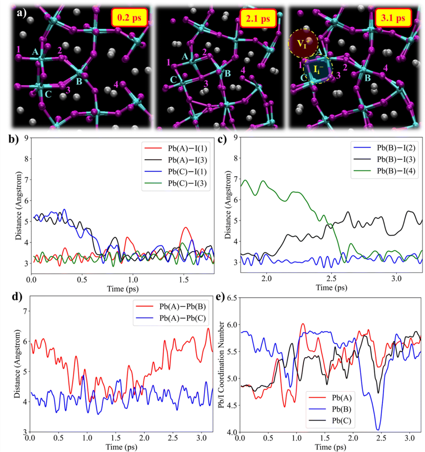 | ||
| Fig. 3 (a) Formation of an iodine Frenkel defect within the center GB. Letters and numbers consistently label the Pb and the I ions, respectively, which are relevant for the formation of the Frenkel defect. The Frenkel defect is highlighted in the right panel (b) and (c) give the time evolution of the Pb–I distances. (d) Time evolution of the Pb–Pb distances between the relevant Pb ions. (e) Time evolution of the Pb/I coordination number for each Pb ion. | ||
To understand the consequence of the Frenkel pair formation within the initial phase of the trajectory, we compare the time evolution of the radial distribution function, g(r), and its integral, int[g(r)], between the respective ions in the center GB, Fig. S9, (see Fig. S10 and S11, ESI,† for g(r) in top/bot GB) and the bulk g(r). Initially, the Pb/Pb int[g(r)] shows a substantial contribution at 4 Å due to the presence of split interstitials. With increasing simulation time, the Pb/Pb and I/Pb g(r) approach an amorphous phase at ∼2 ps in between the bulk and the PbI2g(r) (taken from ref. 60), caused by the increased formation of split interstitials in the GB region. Afterward, the Frenkel pair formation leads to a decreased number of split interstitials. Simultaneously, Pb/Pb and I/Pb g(r) approach the bulk g(r). As a result, the coordination number between the ions in the center GB clearly approach the bulk values, Fig. S12 and S13, ESI.†
The structural changes in the GB arise as a response to the local strain at the junction between grains. Iodine Frenkel pairs form in the GB and bridge the two grains to release the strain and restore the perovskite structure. The formation of Frenkel pairs is supported by iodine migration and the formation of lead–iodine bonds with undercoordinated Pb ions. A salient feature revealed by our AIMD simulations is the observation of Pb migration in the GB. Although Pb migration in the bulk is unexpected due to large activation energies,22 nucleophilic attacks by I− ions from the CsI-terminated region to undercoordinated Pb2+ centers from the PbI-terminated region drive the migration of Pb ions within the GB. Our observations indicate the spontaneous, halide-driven structural healing of the MHP GB at finite temperatures. The soft nature of the MHP lattice combined with low ion migration barriers may be the key to moderate defect densities and the unexpected electronically benign nature of GBs under operational conditions in low-temperature processed MHP thin films. We may hypothesize that aging of MHPs allows the spontaneous healing of grains and potential grain growth. Low-temperature annealing and light-soaking are expected to further support the healing of GBs as ion migration barriers are lowered. The observed self-healing mechanism can explain previous observations of spontaneous crystal coalescence in MHP thin films which were stored in the dark and at room temperature.65 On long timescales, ion migration can enter the grain interior and heal defect states.24 Additionally, light-soaking led to a brightening of grains and annihilation of Frenkel defects within thin films and single crystals which was attributed to iodine migration,66–68 being in line with our observations. Recent studies further reported enhanced migration of chlorine interstitials in GBs,69 a reduction of activation energies for bromine ion migration in small grains in polycrystalline MAPbBr3 films,70 and observed facile migration of iodine interstitials at MAPbI3/MoS2 interfaces to passivate sulfur vacancies.71 Consequently, our observations should be of interest for a large range of lead-halide perovskites, while quantitative differences are expected.
We now investigate the formation mechanism and the type of split interstitials appearing at 6 ps of simulation time near the bulk region, Fig. 2a. The split interstitial forms within the equatorial Pb–I plane located one unit cell above the GB junction and is accompanied by an iodine vacancy, Fig. 4a. The fluctuations of the Pb–I bonds in the GB regions substantially affect the adjacent unit cells and finally lead to the Pb(C)–I(3) bond breaking at 6 ps, as visible from the rapid increase in the Pb(C)–I(3) distance, Fig. S14, ESI.† As an immediate consequence, I(2) rotates around Pb(B) and approaches Pb(A). I(3) takes the position of I(2), and I(2) forms a bond with Pb(B) at 6.8 ps, Fig. 4a. Simultaneously, the Pb(A)–Pb(B) distance drops to ∼4.6 Å. While proposed by several DFT calculations,39,46,67 this is to our knowledge the first observation of a spontaneous iodine Frenkel defect formation in MHP bulk and GBs. To estimate the iodine Frenkel defect formation energy, we construct the Frenkel defect observed from AIMD simulations within the low energy GB structure, Fig. S15c, ESI,† and optimize the ionic positions. DFT calculations predict a Frenkel formation energy of 0.43 eV at the GB region, being substantially lower compared to the bulk (1.01 eV) while being higher compared to the surface (0.11 eV), Fig. 4b. As a consequence, enhanced iodine migration in the GB leads to the facile formation of iodine Frenkel defects. Other studies on Frenkel defects reported formation energies in MHP bulk of 0.86 eV in MAPbI3 (ref. 39) and 0.84 eV in CsPbI3,72 while being substantially reduced at MHP surfaces with values of −0.03 eV to 0.19 eV.39,73 This should lead to enhanced defect concentration in the presence of GBs, while potentially being moderate due to iodine-driven healing as reported above and in literature.24,67,68 The presence of GBs and the accompanied facile formation of mobile iodine point defects can further induce chemical degradation and hamper the stability of PSCs.7,11,24,74 Surface passivation is a commonly used strategy to suppress surface defect formation and simultaneously stabilize the perovskite layers.75–77 The passivation of GBs, however, is not as straightforward and, so far, was achieved with limited success. The use of additives or carefully engineered precursor conditions successfully increased grain sizes but could not completely mitigate GB formation.10,33,78 The complex interplay between defect generation and annihilation is potentially one of the crucial challenges to achieving stable MHP thin films.
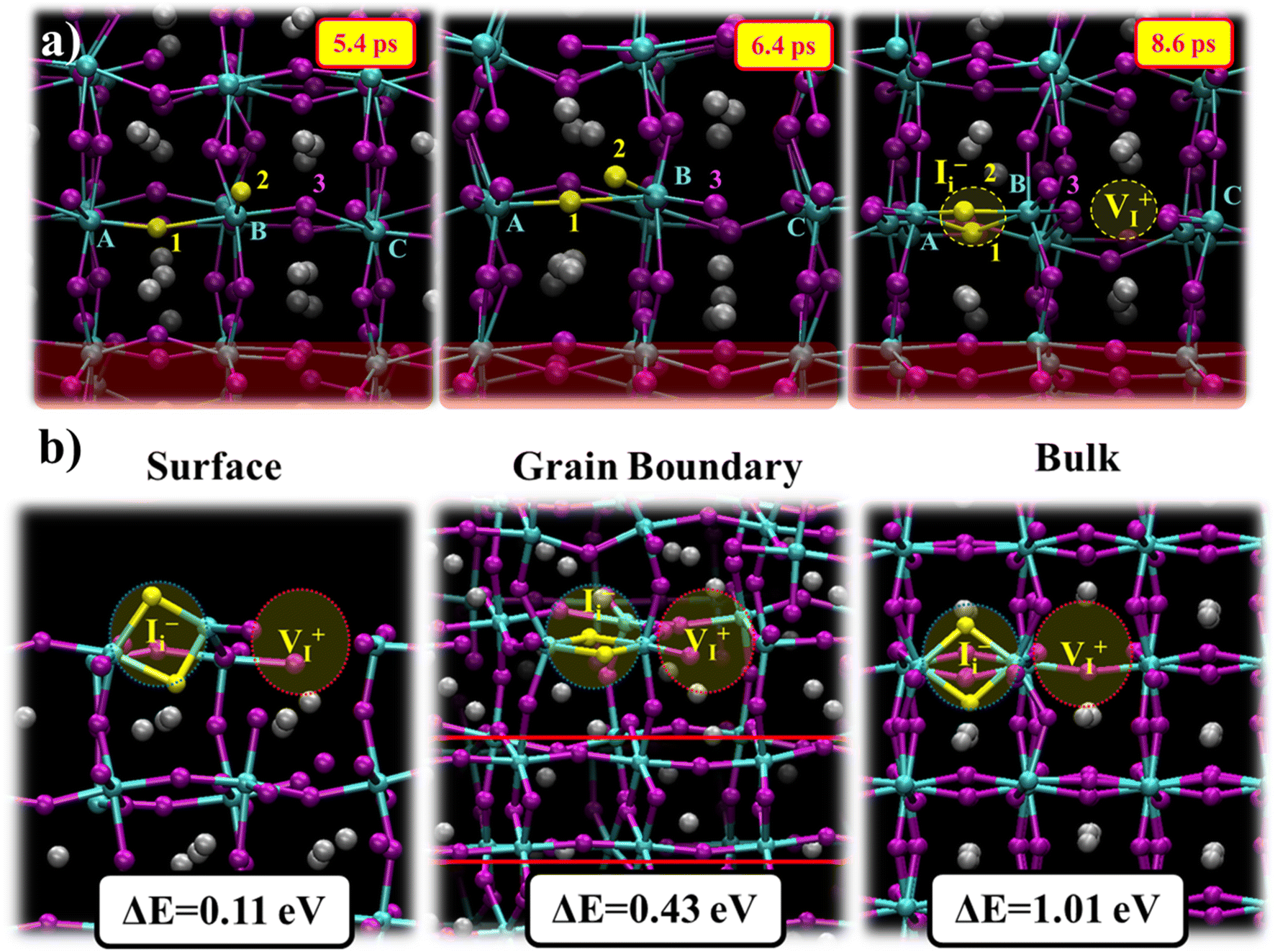 | ||
| Fig. 4 (a) Snapshots visualizing the key steps during the bulk iodine Frenkel defect formation. Letters and numbers consistently label the Pb and the I ions, respectively. The iodine Frenkel defect is highlighted in the right panel. The lower Pb atoms are located at the junction of the GB region, highlighted by the red region. (b) Frenkel formation energy at (left) PbI2-terminated perovskite surface, (mid) at the grain boundary, and (right) in the bulk. | ||
3.2 Electronic properties
We now investigate the electronic properties of the GB under finite temperatures. Several snapshots are extracted from the trajectory, one at every 2 ps of simulation time, and optimized using DFT. We observe a stabilization of the optimized snapshot extracted at 6 ps by 1.03 eV with respect to the initial geometry, Table S2, ESI.† The optimized geometry, Fig. S15, ESI,† preserves the iodine Frenkel pair at the GB, pointing towards high stability of iodine related defects in GBs, as proposed for PbI2-terminated surfaces39 and GBs.44 The density of states (DOS) of the low energy structure shows an opening of the electronic band gap by ∼0.3 eV compared to the initial structure, Fig. S15a, ESI,† while no electronic states in the band gap are observed. Moreover, the HOMO is delocalized within the bulk region, while the LUMO is located at the GB, Fig. S15b, ESI.† Note that we have neglected spin–orbit coupling (SOC) corrections as they are computationally heavy for such large systems; inclusion of SOC reduces the band gap3,79,80 by 1 eV yielding a fair agreement with the experimental band gap of CsPbI3.81We further consider the DOS at finite temperatures by averaging the electronic structure obtained from DFT calculations on several AIMD geometries, Fig. 5a. DOS and HOMO/LUMO orbitals for each snapshot are shown in ESI Movie SM1.† We observe shallow electronic states near the conduction band minimum (CBM), with energies down to ∼300 meV below the CBM. The averaged LUMO is localized at the top/bot GB, while the HOMO is fairly homogeneously spread across the supercell. We observe that the shallow trap states are made of Pb–Pb bonding states (Fig. S16, ESI†), which are stabilized by the increased strain at the GBs while being unstable in perovskite bulk.64 Similar observations were made in previous studies on vacant MAPbI3 surfaces,82 in defective MAPbCl3 due to the reduced lattice parameter with respect to MAPbI3,83 and also in defective bulk MAPbI3 under finite temperatures.84 All studies commonly share the observation that lattice distortion or strain pushes unsaturated Pb ions together which creates Pb–Pb bonding states within the bandgap. Altogether, this may explain the presence of electron trap states at GBs observed in previous experiments.18,85–87 Between 1 ps and 2 ps, electron and hole localization can be observed at the center GB, Fig. 5b, with hole and electron trap states in the DOS, Fig. S17a, ESI.† Consequently, the structural rearrangement accompanied by the iodine Frenkel formation especially mitigates hole trapping at GBs. Ground state DFT calculations predict an electronically benign nature of GBs, while at finite temperatures, electron trap states at the GB may promote charge trapping and non-radiative recombination. Further annealing of the GB can suppress charge trapping at the center GB, which is a key property to ensure high performance in polycrystalline PSCs. Recently proposed passivation strategies for GB defects include alkali metals,34,88 chlorine doping,40,89,90 or Lewis bases.91,92
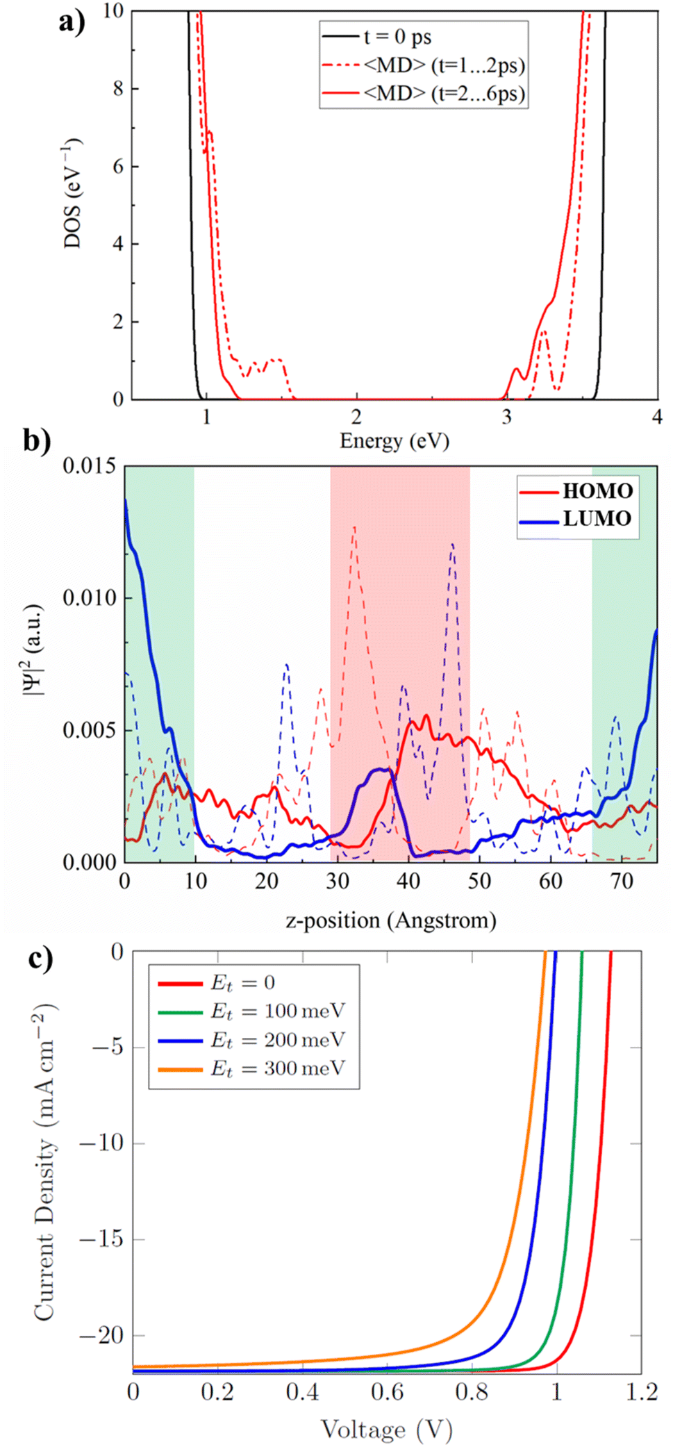 | ||
| Fig. 5 (a) Density of states of the ground state of the initial geometry (black curve) and the thermal averaged AIMD structures (red curve) over 40 (10) snapshots between t = 2 ps and 6 ps (dashed: t = 1 ps and 2 ps) using hybrid DFT calculations. The pDOS for each snapshot as well as the HOMO and LUMO orbitals are given in the movie SM1, ESI.† (b) Probability distribution |ψ|2 for the HOMO and the LUMO averaged from 1 to 2 ps (dashed curve) and from 2 ps to 6 ps the snapshots across the z-position of the supercell. The GB regions are highlighted in red and green for the center and the top/bottom GB, respectively. (c) DD simulation of current density–voltage curves for a model PSC including trap states of density 1016 cm−3 at GB regions with varying trap energy level Et below the CBM. | ||
We further perform drift-diffusion (DD) simulations on a model PSC, using our previous parametrization of MAPbI3,93 to estimate the impact of the observed shallow trap states on the device performance. GBs are modeled as 2 nm wide regions within an effective 1D model of the perovskite absorber, see Fig. S19, ESI.† The effect of GBs is captured by electron traps with varying trap densities and trap energy levels (see Section S3, ESI† for model details) in line with previous device modeling studies.18 To understand the potential role of shallow electron traps near the CBM, we fix the trap density at moderate values of 1016 cm−3 and vary the energy level Et within the range of 0 to 300 meV below the CBM according to our DFT results. For Et = 0 meV (reference), high short-circuit current density (Jsc) of 21.8 mA cm−2 is observed with open-circuit voltage (Voc) of 1.12 V. When Et increases from 0 to 300 meV below CBM, Voc reduces to 0.97 V while Jsc remains nearly unchanged (21.6 mA cm−2). The decrease in Voc can be attributed to increased trap-assisted recombination of charge carriers. Due to the reduced voltage and current density, the maximum power point shifts to the lower values of current and voltage, resulting in poor efficiency of the cell. Overall, the photovoltaic performance deteriorates with an increase in the trap density and the trap energy with respect to the CBM at GBs (see Fig. S20 to S23, ESI,† for different trap densities and energies). Even though being shallow traps, our DD simulations raise the need for the passivation of GB trap states to minimize voltage losses for high performance PSCs.
4. Conclusion
To conclude, we investigated the defect formation and healing at GBs of lead-halide perovskites from first-principles simulations on the prototypical Σ5[130] CsPbI3 GB. Ab initio molecular dynamics simulations show healing of GB defects by the migration of iodine ions, which evolves toward a stabilized GB with reduced charge trap states as a response to the local strain. DFT calculations reveal the presence of shallow electron trap states in the GB, given by strain-induced Pb–Pb bonding states, which mainly hamper the open-circuit voltage by enhanced non-radiative recombination, as presented from drift-diffusion simulations. In contrast, we also observe the formation of iodine Frenkel defects near lead-iodine rich GB regions. DFT calculations predict Frenkel formation energies at surface (0.1 eV) < GB (0.4 eV) < bulk (1.0 eV), suggesting an enhanced defect density due to GBs. Both defect formation and healing are connected to the facile motion of iodine ions inside the GB. Our results propose that the spontaneous healing by the migration of iodine ions may be the key to the surprising success and high performance of polycrystalline perovskite solar cells. Still, the demonstrated controversy between defect formation and healing remains an open issue to be addressed to achieve stable MHP thin films. Thus, we may highlight that the use of additives and the control of the stoichiometry at GBs may further mitigate defect formation to increase both stability and photovoltaic performance. In summary, we believe that the presented atomistic details of the defect formation and healing mechanisms should be helpful to deepen our understanding of GB in perovskites and to derive novel strategies for tailored stability and optoelectronic quality of lead-halide perovskites.Conflicts of interest
There are no conflicts of interest to declare.Acknowledgements
The Ministero dell'Istruzione dell'Università e della Ricerca (MIUR) and Università degli Studi di Perugia are acknowledged for financial support through the program “Dipartimenti di Eccellenza 2018–2022” (Grant AMIS) to F. D. A. W. K, E. M and F. D. A. further acknowledge funding by the PON project “Tecnologia per celle solari bifacciali ad alta Efficienza a 4 terminali per utility scale” (BEST-4U) of the Italian Ministry MIUR (CUP B88D1900016005). E. M. and A. A. A. wish to thank the Distinguished Scientist Fellowship Program (DSFP) of King Saud University, Riyadh, Kingdom of Saudi Arabia. A. G. acknowledges the European Union's Horizon 2020 FETOPEN 2018–2020 program “LION-HEARTED” under grant agreement no. 828984, TUM Innovation Network for Artificial Intelligence powered Multifunctional Material Design (ARTEMIS) and the Deutsche Forschungsgemeinschaft (DFG, German Research Foundation) under Germany's Excellence Strategy – EXC 2089/1 – 390776260 (e-conversion).References
- M. B. Johnston and L. M. Herz, Hybrid Perovskites for Photovoltaics: Charge-Carrier Recombination, Diffusion, and Radiative Efficiencies, Acc. Chem. Res., 2016, 49(1), 146–154, DOI:10.1021/acs.accounts.5b00411.
- S. D. Stranks, G. E. Eperon, G. Grancini, C. Menelaou, M. J. P. Alcocer, T. Leijtens, L. M. Herz, A. Petrozza and H. J. Snaith, Electron-Hole Diffusion Lengths Exceeding 1 Micrometer in an Organometal Trihalide Perovskite Absorber, Science, 2013, 342(6156), 341–344, DOI:10.1126/science.1243982.
- P. Umari, E. Mosconi and F. De Angelis, Relativistic GW Calculations on CH3NH3PbI3 and CH3NH3SnI3 Perovskites for Solar Cell Applications, Sci. Rep., 2014, 4, 4467, DOI:10.1038/srep04467.
- J. Jeong, M. Kim, J. Seo, H. Lu, P. Ahlawat, A. Mishra, Y. Yang, M. A. Hope, F. T. Eickemeyer, M. Kim, Y. J. Yoon, I. W. Choi, B. P. Darwich, S. J. Choi, Y. Jo, J. H. Lee, B. Walker, S. M. Zakeeruddin, L. Emsley, U. Rothlisberger, A. Hagfeldt, D. S. Kim, M. Grätzel and J. Y. Kim, Pseudo-Halide Anion Engineering for α-FAPbI3 Perovskite Solar Cells, Nature, 2021, 592(7854), 381–385, DOI:10.1038/s41586-021-03406-5.
- A. Al-Ashouri, E. Köhnen, B. Li, A. Magomedov, H. Hempel, P. Caprioglio, J. A. Marquez, A. B. M. Vliches, E. Kasparavicius, J. A. Smith, N. Phung, D. Menzel, M. Grischek, L. Kegelmann, D. Skroblin, C. Gollwitzer, T. Malinauskas, J. Marko, G. Matic, B. Rech, R. Schlatmann, M. Topic, L. Korte, A. Abate, B. Stannowksi, D. Neher, M. Stolterfoht, T. Unold, V. Getautis and S. Albrecht, Monolithic Perovskite/Silicon Tandem Solar Cell with >29% Efficiency by Enhanced Hole Extraction, Science, 2020,(370), 1300–1309 CrossRef CAS PubMed.
- D. Meggiolaro, S. G. Motti, E. Mosconi, A. J. Barker, J. Ball, C. Andrea Riccardo Perini, F. Deschler, A. Petrozza and F. De Angelis, Iodine Chemistry Determines the Defect Tolerance of Lead-Halide Perovskites, Energy Environ. Sci., 2018, 11(3), 702–713, 10.1039/C8EE00124C.
- K. Domanski, B. Roose, T. Matsui, M. Saliba, S.-H. Turren-Cruz, J.-P. Correa-Baena, C. R. Carmona, G. Richardson, J. M. Foster, F. De Angelis, J. M. Ball, A. Petrozza, N. Mine, M. K. Nazeeruddin, W. Tress, M. Grätzel, U. Steiner, A. Hagfeldt and A. Abate, Migration of Cations Induces Reversible Performance Losses over Day/Night Cycling in Perovskite Solar Cells, Energy Environ. Sci., 2017, 10(2), 604–613, 10.1039/C6EE03352K.
- O. Yaffe, Y. Guo, L. Z. Tan, D. A. Egger, T. Hull, C. C. Stoumpos, F. Zheng, T. F. Heinz, L. Kronik, M. G. Kanatzidis, J. S. Owen, A. M. Rappe, M. A. Pimenta and L. E. Brus, Local Polar Fluctuations in Lead Halide Perovskite Crystals, Phys. Rev. Lett., 2017, 118(13), 136001, DOI:10.1103/PhysRevLett.118.136001.
- C. Quarti, E. Mosconi and F. De Angelis, Interplay of Orientational Order and Electronic Structure in Methylammonium Lead Iodide: Implications for Solar Cell Operation, Chem. Mater., 2014, 26(22), 6557–6569, DOI:10.1021/cm5032046.
- H. Fan, J.-H. Huang, L. Chen, Y. Zhang, Y. Wang, C. Gao, P. Wang, X. Zhou, K.-J. Jiang and Y. Song, Methylamine-Assisted Secondary Grain Growth for CH3NH3PbI3 Perovskite Films with Large Grains and a Highly Preferred Orientation, J. Mater. Chem. A, 2021, 9(12), 7625–7630, 10.1039/D0TA11916D.
- N. Phung and A. Abate, The Impact of Nano- and Microstructure on the Stability of Perovskite Solar Cells, Small, 2018, 14(46), e1802573, DOI:10.1002/smll.201802573.
- B. Conings, J. Drijkoningen, N. Gauquelin, A. Babayigit, J. D'Haen, L. D'Olieslaeger, A. Ethirajan, J. Verbeeck, J. Manca, E. Mosconi, F. De Angelis and H.-G. Boyen, Intrinsic Thermal Instability of Methylammonium Lead Trihalide Perovskite, Adv. Energy Mater., 2015, 5(15), 1500477, DOI:10.1002/aenm.201500477.
- A. F. Akbulatov, S. A. Tsarev, M. Elshobaki, S. Y. Luchkin, I. S. Zhidkov, E. Z. Kurmaev, S. M. Aldoshin, K. J. Stevenson and P. A. Troshin, Comparative Intrinsic Thermal and Photochemical Stability of Sn(II) Complex Halides as Next-Generation Materials for Lead-Free Perovskite Solar Cells, J. Phys. Chem. C, 2019, 123(44), 26862–26869, DOI:10.1021/acs.jpcc.9b09200.
- W. Kaiser, D. Ricciarelli, E. Mosconi, A. A. Alothman, F. Ambrosio and F. De Angelis, Stability of Tin- versus Lead-Halide Perovskites: Ab Initio Molecular Dynamics Simulations of Perovskite/Water Interfaces, J. Phys. Chem. Lett., 2022, 13(10), 2321–2329, DOI:10.1021/acs.jpclett.2c00273.
- S. Heo, G. Seo, Y. Lee, D. Lee, M. Seol, J. Lee, J.-B. Park, K. Kim, D.-J. Yun, Y. S. Kim, J. K. Shin, T. K. Ahn and M. K. Nazeeruddin, Deep Level Trapped Defect Analysis in CH3NH3PbI3 Perovskite Solar Cells by Deep Level Transient Spectroscopy, Energy Environ. Sci., 2017, 10(5), 1128–1133, 10.1039/C7EE00303J.
- W. Chu, W. A. Saidi, J. Zhao and O. V. Prezhdo, Soft Lattice and Defect Covalency Rationalize Tolerance of β-CsPbI3 Perovskite Solar Cells to Native Defects, Angew. Chem., Int. Ed., 2020, 59(16), 6435–6441, DOI:10.1002/anie.201915702.
- W. Chu, Q. Zheng, O. V. Prezhdo, J. Zhao and W. A. Saidi, Low-Frequency Lattice Phonons in Halide Perovskites Explain High Defect Tolerance toward Electron-Hole Recombination, Sci. Adv., 2020, 6(7), eaaw7453, DOI:10.1126/sciadv.aaw7453.
- T. S. Sherkar, C. Momblona, L. Gil-Escrig, J. Ávila, M. Sessolo, H. J. Bolink and L. J. A. Koster, Recombination in Perovskite Solar Cells: Significance of Grain Boundaries, Interface Traps, and Defect Ions, ACS Energy Lett., 2017, 2(5), 1214–1222, DOI:10.1021/acsenergylett.7b00236.
- A.-F. Castro-Méndez, J. Hidalgo and J.-P. Correa-Baena, The Role of Grain Boundaries in Perovskite Solar Cells, Adv. Energy Mater., 2019, 9(38), 1901489, DOI:10.1002/aenm.201901489.
- J.-P. Correa-Baena, M. Anaya, G. Lozano, W. Tress, K. Domanski, M. Saliba, T. Matsui, T. J. Jacobsson, M. E. Calvo, A. Abate, M. Grätzel, H. Míguez and A. Hagfeldt, Unbroken Perovskite: Interplay of Morphology, Electro-optical Properties, and Ionic Movement, Adv. Mater., 2016, 28(25), 5031–5037, DOI:10.1002/adma.201600624.
- Y. Shao, Y. Fang, T. Li, Q. Wang, Q. Dong, Y. Deng, Y. Yuan, H. Wei, M. Wang, A. Gruverman, J. Shield and J. Huang, Grain Boundary Dominated Ion Migration in Polycrystalline Organic–Inorganic Halide Perovskite Films, Energy Environ. Sci., 2016, 9(5), 1752–1759, 10.1039/C6EE00413J.
- J. M. Azpiroz, E. Mosconi, J. Bisquert and F. De Angelis, Defect Migration in Methylammonium Lead Iodide and its Role in Perovskite Solar Cell Operation, Energy Environ. Sci., 2015, 8(7), 2118–2127, 10.1039/C5EE01265A.
- C. Eames, J. M. Frost, P. R. F. Barnes, B. C. O'Regan, A. Walsh and M. S. Islam, Ionic Transport in Hybrid Lead Iodide Perovskite Solar Cells, Nat. Commun., 2015, 6, 7497, DOI:10.1038/ncomms8497.
- N. Phung, A. Al-Ashouri, S. Meloni, A. Mattoni, S. Albrecht, E. L. Unger, A. Merdasa and A. Abate, The Role of Grain Boundaries on Ionic Defect Migration in Metal Halide Perovskites, Adv. Energy Mater., 2020, 10(20), 1903735, DOI:10.1002/aenm.201903735.
- A. Mattoni and S. Meloni, Defect Dynamics in MAPbI3 Polycrystalline Films: The Trapping Effect of Grain Boundaries, Helv. Chim. Acta, 2020, 103(9), e2000110, DOI:10.1002/hlca.202000110.
- T. Leijtens, G. E. Eperon, A. J. Barker, G. Grancini, W. Zhang, J. M. Ball, A. R. S. Kandada, H. J. Snaith and A. Petrozza, Carrier Trapping and Recombination: The Role of Defect Physics in Enhancing the Open Circuit Voltage of Metal Halide Perovskite Solar Cells, Energy Environ. Sci., 2016, 9(11), 3472–3481, 10.1039/C6EE01729K.
- S. Kosar, A. J. Winchester, T. A. S. Doherty, S. Macpherson, C. E. Petoukhoff, K. Frohna, M. Anaya, N. S. Chan, J. Madéo, M. K. L. Man, S. D. Stranks and K. M. Dani, Unraveling the Varied Nature and Roles of Defects in Hybrid Halide Perovskites with Time-Resolved Photoemission Electron Microscopy, Energy Environ. Sci., 2021,(14), 6320–6328, 10.1039/D1EE02055B.
- D. W. deQuilettes, S. M. Vorpahl, S. D. Stranks, H. Nagaoka, G. E. Eperon, M. E. Ziffer, H. J. Snaith and D. S. Ginger, Impact of Microstructure on Local Carrier Lifetime in Perovskite Solar Cells, Science, 2015, 348(6235), 683–686, DOI:10.1126/science.aaa5333.
- T. A. S. Doherty, A. J. Winchester, S. Macpherson, D. N. Johnstone, V. Pareek, E. M. Tennyson, S. Kosar, F. U. Kosasih, M. Anaya, M. Abdi-Jalebi, Z. Andaji-Garmaroudi, E. L. Wong, J. Madéo, Y.-H. Chiang, J.-S. Park, Y.-K. Jung, C. E. Petoukhoff, G. Divitini, M. K. L. Man, C. Ducati, A. Walsh, P. A. Midgley, K. M. Dani and S. D. Stranks, Performance-Limiting Nanoscale Trap Clusters at Grain Junctions in Halide Perovskites, Nature, 2020, 580(7803), 360–366, DOI:10.1038/s41586-020-2184-1.
- S. Jariwala, H. Sun, G. W. Adhyaksa, A. Lof, L. A. Muscarella, B. Ehrler, E. C. Garnett and D. S. Ginger, Local Crystal Misorientation Influences Non-radiative Recombination in Halide Perovskites, Joule, 2019, 3(12), 3048–3060, DOI:10.1016/j.joule.2019.09.001.
- Q. Sun, P. Fassl, D. Becker-Koch, A. Bausch, B. Rivkin, S. Bai, P. E. Hopkinson, H. J. Snaith and Y. Vaynzof, Role of Microstructure in Oxygen Induced Photodegradation of Methylammonium Lead Triiodide Perovskite Films, Adv. Energy Mater., 2017, 7(20), 1700977, DOI:10.1002/aenm.201700977.
- Q. Wang, B. Chen, Y. Liu, Y. Deng, Y. Bai, Q. Dong and J. Huang, Scaling Behavior of Moisture-Induced Grain Degradation in Polycrystalline Hybrid Perovskite Thin Films, Energy Environ. Sci., 2017, 10(2), 516–522, 10.1039/C6EE02941H.
- C. Wang, Z. Song, D. Zhao, R. A. Awni, C. Li, N. Shrestha, C. Chen, X. Yin, D. Li, R. J. Ellingson, X. Zhao, X. Li and Y. Yan, Improving Performance and Stability of Planar Perovskite Solar Cells through Grain Boundary Passivation with Block Copolymers, Sol. RRL, 2019, 3(9), 1900078, DOI:10.1002/solr.201900078.
- L. Qiao, W.-H. Fang, R. Long and O. V. Prezhdo, Atomic Model for Alkali Metal Passivation of Point Defects at Perovskite Grain Boundaries, ACS Energy Lett., 2020, 5(12), 3813–3820, DOI:10.1021/acsenergylett.0c02136.
- D. Liu, D. Luo, A. N. Iqbal, K. W. P. Orr, T. A. S. Doherty, Z.-H. Lu, S. D. Stranks and W. Zhang, Strain Analysis and Engineering in Halide Perovskite Photovoltaics, Nat. Mater., 2021, 20(10), 1337–1346, DOI:10.1038/s41563-021-01097-x.
- J.-S. Park and A. Walsh, Modeling Grain Boundaries in Polycrystalline Halide Perovskite Solar Cells, Annu. Rev. Condens. Matter Phys., 2021, 12(1), 95–109, DOI:10.1146/annurev-conmatphys-042020-025347.
- M. U. Rothmann, J. S. Kim, J. Borchert, K. B. Lohmann, C. M. O’Leary, A. A. Sheader, L. Clark, H. J. Snaith, M. B. Johnston, P. D. Nellist and L. M. Herz, Atomic-Scale Microstructure of Metal Halide Perovskite, Science, 2020, 370(6516), eabb5940, DOI:10.1126/science.abb5940.
- D. Yang, W. Ming, H. Shi, L. Zhang and M.-H. Du, Fast Diffusion of Native Defects and Impurities in Perovskite Solar Cell Material CH3NH3PbI3, Chem. Mater., 2016, 28(12), 4349–4357, DOI:10.1021/acs.chemmater.6b01348.
- D. Meggiolaro, E. Mosconi and F. De Angelis, Formation of Surface Defects Dominates Ion Migration in Lead-Halide Perovskites, ACS Energy Lett., 2019, 4(3), 779–785, DOI:10.1021/acsenergylett.9b00247.
- R. Long, J. Liu and O. V. Prezhdo, Unravelling the Effects of Grain Boundary and Chemical Doping on Electron-Hole Recombination in CH3NH3PbI3 Perovskite by Time-Domain Atomistic Simulation, J. Am. Chem. Soc., 2016, 138(11), 3884–3890, DOI:10.1021/jacs.6b00645.
- Y. Wang, W.-H. Fang, R. Long and O. V. Prezhdo, Symmetry Breaking at MAPbI3 Perovskite Grain Boundaries Suppresses Charge Recombination: Time-Domain ab Initio Analysis, J. Phys. Chem. Lett., 2019, 10(7), 1617–1623, DOI:10.1021/acs.jpclett.9b00763.
- Y. Guo, Q. Wang and W. A. Saidi, Structural Stabilities and Electronic Properties of High-Angle Grain Boundaries in Perovskite Cesium Lead Halides, J. Phys. Chem. C, 2017, 121(3), 1715–1722, DOI:10.1021/acs.jpcc.6b11434.
- W. Shan and W. A. Saidi, Segregation of Native Defects to the Grain Boundaries in Methylammonium Lead Iodide Perovskite, J. Phys. Chem. Lett., 2017, 8(23), 5935–5942, DOI:10.1021/acs.jpclett.7b02727.
- J.-S. Park, J. Calbo, Y.-K. Jung, L. D. Whalley and A. Walsh, Accumulation of Deep Traps at Grain Boundaries in Halide Perovskites, ACS Energy Lett., 2019, 4(6), 1321–1327, DOI:10.1021/acsenergylett.9b00840.
- A. Marronnier, G. Roma, S. Boyer-Richard, L. Pedesseau, J.-M. Jancu, Y. Bonnassieux, C. Katan, C. C. Stoumpos, M. G. Kanatzidis and J. Even, Anharmonicity and Disorder in the Black Phases of Cesium Lead Iodide Used for Stable Inorganic Perovskite Solar Cells, ACS Nano, 2018, 12(4), 3477–3486, DOI:10.1021/acsnano.8b00267.
- E. Mosconi and F. De Angelis, Mobile Ions in Organohalide Perovskites: Interplay of Electronic Structure and Dynamics, ACS Energy Lett., 2016, 1(1), 182–188, DOI:10.1021/acsenergylett.6b00108.
- W. Kaiser, M. Carignano, A. A. Alothman, E. Mosconi, A. Kachmar, W. A. Goddard and F. De Angelis, First-Principles Molecular Dynamics in Metal-Halide Perovskites: Contrasting Generalized Gradient Approximation and Hybrid Functionals, J. Phys. Chem. Lett., 2021, 12(49), 11886–11893, DOI:10.1021/acs.jpclett.1c03428.
- R. Car and M. Parrinello, Unified Approach for Molecular Dynamics and Density-Functional Theory, Phys. Rev. Lett., 1985, 55, 2471–2474, DOI:10.1103/PhysRevLett.55.2471.
- J. Hutter, Car-Parrinello Molecular Dynamics, Wiley Interdiscip. Rev.: Comput. Mol. Sci., 2012, 2(4), 604–612, DOI:10.1002/wcms.90.
- M. E. Tuckerman, Ab Initio Molecular Dynamics: Basic Concepts, Current Trends and Novel Applications, J. Phys.: Condens. Matter, 2002, 14(50), R1297–R1355, DOI:10.1088/0953-8984/14/50/202.
- P. Giannozzi, S. Baroni, N. Bonini, M. Calandra, R. Car, C. Cavazzoni, D. Ceresoli, G. L. Chiarotti, M. Cococcioni, I. Dabo, A. Dal Corso, S. d. Gironcoli, S. Fabris, G. Fratesi, R. Gebauer, U. Gerstmann, C. Gougoussis, A. Kokalj, M. Lazzeri, L. Martin-Samos, N. Marzari, F. Mauri, R. Mazzarello, S. Paolini, A. Pasquarello, L. Paulatto, C. Sbraccia, S. Scandolo, G. Sclauzero, A. P. Seitsonen, A. Smogunov, P. Umari and R. M. Wentzcovitch, QUANTUM ESPRESSO: A Modular and Open-Source Software Project for Quantum Simulations of Materials, J. Phys.: Condens. Matter, 2009, 21(39), 395502, DOI:10.1088/0953-8984/21/39/395502.
- J. P. Perdew, K. Burke and M. Ernzerhof, Generalized Gradient Approximation Made Simple, Phys. Rev. Lett., 1996, 77(18), 3865–3868, DOI:10.1103/PhysRevLett.77.3865.
- S. Ratanaphan, Y. Yoon and G. S. Rohrer, The Five Parameter Grain Boundary Character Distribution of Polycrystalline Silicon, J. Mater. Sci., 2014, 49(14), 4938–4945, DOI:10.1007/s10853-014-8195-2.
- J.-S. Park, J. Kang, J.-H. Yang, W. Metzger and S.-H. Wei, Stability and Electronic Structure of the Low-Σ Grain Boundaries in CdTe: A Density Functional Study, New J. Phys., 2015, 17(1), 13027, DOI:10.1088/1367-2630/17/1/013027.
- J. A. Dawson, P. Canepa, T. Famprikis, C. Masquelier and M. S. Islam, Atomic-Scale Influence of Grain Boundaries on Li-Ion Conduction in Solid Electrolytes for All-Solid-State Batteries, J. Am. Chem. Soc., 2018, 140(1), 362–368, DOI:10.1021/jacs.7b10593.
- T. D. Kühne, M. Iannuzzi, M. D. Ben, V. V. Rybkin, P. Seewald, F. Stein, T. Laino, R. Z. Khaliullin, O. Schütt, F. Schiffmann, D. Golze, J. Wilhelm, S. Chulkov, M. H. Bani-Hashemian, V. Weber, U. Borstnik, M. Taillefumier, A. S. Jakobovits, A. Lazzaro, H. Pabst, T. Müller, R. Schade, M. Guidon, S. Andermatt, N. Holmberg, G. K. Schenter, A. Hehn, A. Bussy, F. Belleflamme, G. Tabacchi, A. Glöβ, M. Lass, I. Bethune, C. J. Mundy, C. Plessl, M. Watkins, J. VandeVondele, M. Krack and J. Hutter, CP2K: An Electronic Structure and Molecular Dynamics Software Package - Quickstep: Efficient and Accurate Electronic Structure Calculations, J. Chem. Phys., 2020, 152(19), 194103, DOI:10.1063/5.0007045.
- S. Goedecker, M. Teter and J. Hutter, Separable Dual-Space Gaussian Pseudopotentials, Phys. Rev. B: Condens. Matter Mater. Phys., 1996, 54(3), 1703–1710 CrossRef CAS PubMed.
- J. VandeVondele and J. Hutter, Gaussian Basis Sets for Accurate Calculations on Molecular Systems in Gas and Condensed Phases, J. Chem. Phys., 2007, 127(11), 114105, DOI:10.1063/1.2770708.
- M. Guidon, J. Hutter and J. VandeVondele, Auxiliary Density Matrix Methods for Hartree-Fock Exchange Calculations, J. Chem. Theory Comput., 2010, 6(8), 2348–2364, DOI:10.1021/ct1002225.
- W. Kaiser, E. Mosconi, A. A. Alothman, D. Meggiolaro, A. Gagliardi and F. De Angelis, Halide-Driven Formation of Lead Halide Perovskites: Insight from Ab Initio Molecular Dynamics Simulations, Mater. Adv., 2021, 2, 3915–3926, 10.1039/D1MA00371B.
- P. Ahlawat, M. I. Dar, P. Piaggi, M. Grätzel, M. Parrinello and U. Rothlisberger, Atomistic Mechanism of the Nucleation of Methylammonium Lead Iodide Perovskite from Solution, Chem. Mater., 2020, 32(1), 529–536, DOI:10.1021/acs.chemmater.9b04259.
- C. Caddeo, A. Filippetti and A. Mattoni, The Dominant Role of Surfaces in the Hysteretic Behavior of Hybrid Perovskites, Nano Energy, 2020, 67, 104162, DOI:10.1016/j.nanoen.2019.104162.
- M. Pols, J. M. Vicent-Luna, I. Filot, A. C. T. van Duin and S. Tao, Atomistic Insights Into the Degradation of Inorganic Halide Perovskite CsPbI3: A Reactive Force Field Molecular Dynamics Study, J. Phys. Chem. Lett., 2021, 12(23), 5519–5525, DOI:10.1021/acs.jpclett.1c01192.
- D. Meggiolaro and F. De Angelis, First-Principles Modeling of Defects in Lead Halide Perovskites: Best Practices and Open Issues, ACS Energy Lett., 2018, 3(9), 2206–2222, DOI:10.1021/acsenergylett.8b01212.
- B. Roose, A. Ummadisingu, J.-P. Correa-Baena, M. Saliba, A. Hagfeldt, M. Graetzel, U. Steiner and A. Abate, Spontaneous Crystal Coalescence Enables Highly Efficient Perovskite Solar Cells, Nano Energy, 2017, 39, 24–29, DOI:10.1016/j.nanoen.2017.06.037.
- D. W. deQuilettes, W. Zhang, V. M. Burlakov, D. J. Graham, T. Leijtens, A. Osherov, V. Bulović, H. J. Snaith, D. S. Ginger and S. D. Stranks, Photo-Induced Halide Redistribution in Organic-Inorganic Perovskite Films, Nat. Commun., 2016, 7, 11683, DOI:10.1038/ncomms11683.
- E. Mosconi, D. Meggiolaro, H. J. Snaith, S. D. Stranks and F. De Angelis, Light-Induced Annihilation of Frenkel Defects in Organo-Lead Halide Perovskites, Energy Environ. Sci., 2016, 9(10), 3180–3187, 10.1039/C6EE01504B.
- J. F. Galisteo-López, M. E. Calvo and H. Míguez, Spatially Resolved Analysis of Defect Annihilation and Recovery Dynamics in Metal Halide Perovskite Single Crystals, ACS Appl. Energy Mater., 2019, 2(10), 6967–6972, DOI:10.1021/acsaem.9b01335.
- B. Yang, C. C. Brown, J. Huang, L. Collins, X. Sang, R. R. Unocic, S. Jesse, S. V. Kalinin, A. Belianinov, J. Jakowski, D. B. Geohegan, B. G. Sumpter, K. Xiao and O. S. Ovchinnikova, Enhancing Ion Migration in Grain Boundaries of Hybrid Organic–Inorganic Perovskites by Chlorine, Adv. Funct. Mater., 2017, 27(26), 1700749 CrossRef.
- L. McGovern, I. Koschany, G. Grimaldi, L. A. Muscarella and B. Ehrler, Grain Size Influences Activation Energy and Migration Pathways in MAPbBr3 Perovskite Solar Cells, J. Phys. Chem. Lett., 2021, 12(9), 2423–2428, DOI:10.1021/acs.jpclett.1c00205.
- Y. Shi, O. V. Prezhdo, J. Zhao and W. A. Saidi, Iodine and Sulfur Vacancy Cooperation Promotes Ultrafast Charge Extraction at MAPbI3/MoS2 Interface, ACS Energy Lett., 2020, 5(5), 1346–1354, DOI:10.1021/acsenergylett.0c00485.
- R. A. Evarestov, A. Senocrate, E. A. Kotomin and J. Maier, First-Principles Calculations of Iodine-Related Point Defects in CsPbI3, Phys. Chem. Chem. Phys., 2019, 21(15), 7841–7846, 10.1039/c9cp00414a.
- Y. Hassan, J. H. Park, M. L. Crawford, A. Sadhanala, J. Lee, J. C. Sadighian, E. Mosconi, R. Shivanna, E. Radicchi, M. Jeong, C. Yang, H. Choi, S. H. Park, M. H. Song, F. De Angelis, C. Y. Wong, R. H. Friend, B. R. Lee and H. J. Snaith, Ligand-Engineered Bandgap Stability in Mixed-Halide Perovskite LEDs, Nature, 2021, 591(7848), 72–77, DOI:10.1038/s41586-021-03217-8.
- S. Tan, I. Yavuz, M. H. Weber, T. Huang, C.-H. Chen, R. Wang, H.-C. Wang, J. H. Ko, S. Nuryyeva, J. Xue, Y. Zhao, K.-H. Wei, J.-W. Lee and Y. Yang, Shallow Iodine Defects Accelerate the Degradation of α-Phase Formamidinium Perovskite, Joule, 2020, 4(11), 2426–2442, DOI:10.1016/j.joule.2020.08.016.
- B. Yang, J. Suo, E. Mosconi, D. Ricciarelli, W. Tress, F. De Angelis, H.-S. Kim and A. Hagfeldt, Outstanding Passivation Effect by a Mixed-Salt Interlayer with Internal Interactions in Perovskite Solar Cells, ACS Energy Lett., 2020, 5(10), 3159–3167, DOI:10.1021/acsenergylett.0c01664.
- S. Yang, S. Chen, E. Mosconi, Y. Fang, X. Xiao, C. Wang, Y. Zhou, J. Zhao, Y. Gao, F. De Angelis and J. Huang, Stabilizing Halide Perovskite Surfaces for Solar Cell Operation with Wide-Bandgap Lead Oxysalts, Science, 2019, 365, 473–478 CrossRef CAS PubMed.
- Q. Jiang, Y. Zhao, X. Zhang, X. Yang, Y. Chen, Z. Chu, Q. Ye, X. Li, Z. Yin and J. You, Surface Passivation of Perovskite Film for Efficient Solar Cells, Nat. Photonics, 2019, 13(7), 460–466, DOI:10.1038/s41566-019-0398-2.
- Y. Xu, L. Zhu, J. Shi, S. Lv, X. Xu, J. Xiao, J. Dong, H. Wu, Y. Luo, D. Li and Q. Meng, Efficient Hybrid Mesoscopic Solar Cells with Morphology-Controlled CH3NH3PbI3−xClx Derived from Two-Step Spin Coating Method, ACS Appl. Mater. Interfaces, 2015, 7(4), 2242–2248, DOI:10.1021/am5057807.
- A. Amat, E. Mosconi, E. Ronca, C. Quarti, P. Umari, M. K. Nazeeruddin, M. Grätzel and F. De Angelis, Cation-Induced Band-Gap Tuning in Organohalide Perovskites: Interplay of Spin-Orbit Coupling and Octahedra Tilting, Nano Lett., 2014, 14(6), 3608–3616, DOI:10.1021/nl5012992.
- J. Even, L. Pedesseau, J.-M. Jancu and C. Katan, Importance of Spin–Orbit Coupling in Hybrid Organic/Inorganic Perovskites for Photovoltaic Applications, J. Phys. Chem. Lett., 2013, 4(17), 2999–3005, DOI:10.1021/jz401532q.
- D. M. Trots and S. V. Myagkota, High-Temperature Structural Evolution of Caesium and Rubidium Triiodoplumbates, J. Phys. Chem. Solids, 2008, 69(10), 2520–2526, DOI:10.1016/j.jpcs.2008.05.007.
- H. Uratani and K. Yamashita, Charge Carrier Trapping at Surface Defects of Perovskite Solar Cell Absorbers: A First-Principles Study, J. Phys. Chem. Lett., 2017, 8(4), 742–746, DOI:10.1021/acs.jpclett.7b00055.
- J. Kim, C.-H. Chung and K.-H. Hong, Understanding of the Formation of Shallow Level Defects from the Intrinsic Defects of Lead Tri-Halide Perovskites, Phys. Chem. Chem. Phys., 2016, 18(39), 27143–27147, 10.1039/c6cp02886a.
- C.-J. Tong, L. Li, L.-M. Liu and O. V. Prezhdo, Synergy between Ion Migration and Charge Carrier Recombination in Metal-Halide Perovskites, J. Am. Chem. Soc., 2020, 142(6), 3060–3068, DOI:10.1021/jacs.9b12391.
- T. Leijtens, S. D. Stranks, G. E. Eperon, R. Lindblad, E. M. J. Johansson, I. J. McPherson, H. Rensmo, J. M. Ball, M. M. Lee and H. J. Snaith, Electronic Properties of Meso-Superstructured and Planar Organometal Halide Perovskite Films: Charge Trapping, Photodoping, and Carrier Mobility, ACS Nano, 2014, 8(7), 7147–7155, DOI:10.1021/nn502115k.
- S. Shao, M. Abdu-Aguye, T. S. Sherkar, H.-H. Fang, S. Adjokatse, G. Brink ten, B. J. Kooi, L. J. A. Koster and M. A. Loi, The Effect of the Microstructure on Trap-Assisted Recombination and Light Soaking Phenomenon in Hybrid Perovskite Solar Cells, Adv. Funct. Mater., 2016, 26(44), 8094–8102, DOI:10.1002/adfm.201602519.
- J.-S. Park, Stabilization and Self-Passivation of Grain Boundaries in Halide Perovskite by Rigid Body Translation, J. Phys. Chem. Lett., 2022, 13(20), 4628–4633, DOI:10.1021/acs.jpclett.2c01123.
- W. Zhao, Z. Yao, F. Yu, D. Yang and S. F. Liu, Alkali Metal Doping for Improved CH3NH3PbI3 Perovskite Solar Cells, Adv. Sci., 2018, 5(2), 1700131, DOI:10.1002/advs.201700131.
- L. Qiao, W.-H. Fang and R. Long, Dual Passivation of Point Defects at Perovskite Grain Boundaries with Ammonium Salts Greatly Inhibits Nonradiative Charge Recombination, J. Phys. Chem. Lett., 2022, 13(4), 954–961, DOI:10.1021/acs.jpclett.1c04038.
- Y. Wang, J. He, Y. Yang, Z. Zhang and R. Long, Chlorine Passivation of Grain Boundary Suppresses Electron–Hole Recombination in CsPbBr3 Perovskite by Nonadiabatic Molecular Dynamics Simulation, ACS Appl. Energy Mater., 2019, 2(5), 3419–3426, DOI:10.1021/acsaem.9b00220.
- Y. Guo, W. Sato, K. Shoyama and E. Nakamura, Sulfamic Acid-Catalyzed Lead Perovskite Formation for Solar Cell Fabrication on Glass or Plastic Substrates, J. Am. Chem. Soc., 2016, 138(16), 5410–5416, DOI:10.1021/jacs.6b02130.
- T. Niu, J. Lu, R. Munir, J. Li, D. Barrit, X. Zhang, H. Hu, Z. Yang, A. Amassian, K. Zhao and S. F. Liu, Stable High-Performance Perovskite Solar Cells via Grain Boundary Passivation, Adv. Mater., 2018, 30(16), e1706576, DOI:10.1002/adma.201706576.
- A. Gagliardi and A. Abate, Mesoporous Electron-Selective Contacts Enhance the Tolerance to Interfacial Ion Accumulation in Perovskite Solar Cells, ACS Energy Lett., 2018, 3, 163–169 CrossRef CAS.
Footnote |
| † Electronic supplementary information (ESI) available: Additional structural analysis: split interstitials in the CsI- and PbI-terminated region; I–I and Pb–Pb distance distribution in the split interstitials; I–I and Pb–Pb distance distribution versus distance to the GBs; iodine interstitial structure in the CsPbI3 bulk; time evolution of the Pb/I coordination number of the individual Pb ions in the center GB; time evolution of the radial pair distribution for I/Pb and Pb/Pb, and the Pb/A and I/A coordination number (A = Pb, I, Cs); electronic and geometric structure of the optimized GB structures; probability distribution of the HOMO and LUMO as function of the z-position in the supercell. Drift-diffusion model and extensive parameter analysis. See DOI: https://doi.org/10.1039/d2ta06336k |
| This journal is © The Royal Society of Chemistry 2022 |