
Unravelling nanostructured Nb-doped TiO2 dual band behaviour in smart windows by in situ spectroscopies†
Miguel
García-Tecedor
 a,
Giulio
Gorni
b,
Freddy
Oropeza
a,
Laura
Gómez
a,
Marta
Liras
a,
Victor A.
de la Peña O'Shea
*a and
Mariam
Barawi
*a
a,
Giulio
Gorni
b,
Freddy
Oropeza
a,
Laura
Gómez
a,
Marta
Liras
a,
Victor A.
de la Peña O'Shea
*a and
Mariam
Barawi
*a
aPhotoactivated Processes Unit, IMDEA Energy Institute, Avda. Ramón de la Sagra, 3, 28935 Móstoles, Madrid, Spain. E-mail: mariam.barawi@imdea.org
bCLÆSS Beamline, CELLS-ALBA Synchrotron, Carrer de la LLum, 2-26, 08290, Cerdanyola del Vallès, Barcelona, Spain
First published on 4th July 2022
Abstract
Nb doped TiO2 nanocrystals (NCs) are one of the most attractive candidates for energy-efficient smart window devices due to their ability to provide a selective modulation of the optical transmittance in the visible and near infrared regions. This dual functionality is associated with two independent bulk (polaronic absorption) and surface (plasmonic absorption) electrochemical charging processes. However, there are still some unclear aspects such as the real role of Nb5+ in the electrochemical reduction of anatase TiO2 and the chemical changes experienced by the dopant during this reaction. Herein, a comprehensive in situ X-ray absorption spectroscopy study has been employed to unveil the more effective reduction of the doped anatase and the significant reduction of the Nb5+ dopant to Nb4+ under electrochemical reaction conditions. Additionally, an exhaustive electrochemical impedance spectroscopy and in situ spectroelectrochemistry study on a lab-scale smart window device sheds light on the dual polaronic and plasmonic charge accumulation processes occurring in these NCs during operation.
 Mariam Barawi | Dr Mariam Barawi is a Senior Assistant researcher at Imdea Energy in charge of the (photo)electrochemical cell line in the Photoactivated Process Unit. She obtained her PhD in 2015 from the Universidad Autónoma de Madrid, investigating solar energy conversion into hydrogen through photoelectrochemical cells. During this period, she was awarded a grant for a research stage under a COST action at Institut de Chimie et des Matériaux in Paris. Thereafter she started her postdoctoral period at Istituto Italiano di Tecnologia investigating inorganic nanocrystals for smart windows application. In January 2017, she joined Imdea Energy and during this period she has been awarded two Spanish government postdoctoral grants (Juan de la Cierva-Formación2017 and a Juan de la Cierva-Incorporación2020). Mariam is co-author of 38 scientific publications at present and has participated in more than 15 research projects funded by different national and international institutions, being Principal Investigator in two of them. |
Introduction
A high control over the solar radiation that enters buildings through systems such as smart windows is a very attractive strategy from the point of view of energy efficiency.1–4 The energy consumption of buildings accounts for around 30% of the world total and they are responsible for 10% of greenhouse gas emissions. In addition, practically half of this energy consumption is used for heating and cooling acclimatization systems.5 In this sense, electrochromic materials offer the possibility of controlling the entrance of the visible part of solar radiation.6–8 However, the radiation that reaches the earth's surface contains, in addition to visible, ultraviolet and infrared radiation in almost equal proportions.9 This is why a large amount of energy is consumed to regulate the temperature inside houses, requiring refrigeration in warm months and heating in cold ones. For this reason, an ideal smart window should be able to independently control the input of visible solar light and the heat provided by the NIR spectrum part according to needs.10 In this line, the so-called dual band electrochromic devices that can selectively filter the transmittance of different regions of the electromagnetic spectrum (VIS and NIR) started to be investigated a few years ago.11,12 Unlike a conventional electrochromic device, they can selectively filter the NIR part, responsible for the heat, from the visible part. For this purpose, one possibility is to use two single band materials as two different independent electrodes, where one filters the NIR and the other the visible.13 There are also examples where a single active electrode, composed of a unique material with a modulated electronic structure via intentional doping, can selectively filter different wavelengths independently by tuning the applied voltage.14–17 This last strategy seems the most attractive alternative from the design point of view as it only implies the use of a single active material.To understand the design and operation of single material devices, it is necessary to clarify the electrochemical reactions behind the introduction of charge carriers that cause the reversible change of their optical features. In this regard, two light absorption mechanisms in different spectral regions can be differentiated: polaronic and plasmonic absorptions.18 The formation of polarons implies an electronic charge localization which is balanced by ion intercalation, producing a faradaic charge. This effect also leads to a distortion in the crystal lattice. Polaronic absorption is responsible for the optical changes in the VIS range exhibited by metal oxides with electrochromic properties. At reduction potentials, a distortion occurs in the oxide network caused by the reduction of the metallic element and the intercalation of the ions in solution (Li+, Na+, etc.). The energetic stabilization during the electron insertion process can result in an electron polaron band below the conduction band edge formation, causing new absorption transitions, mainly in the visible region.19,20 On the other hand, light interaction induces a coherent collective oscillation of free carriers within the NCs, resulting in a localized surface plasmon resonance (LSPR), which can be equilibrated by surface charge or superficial ion intercalation, leading to the formation of an electrochemical double layer.21,22 LSPR is usually exhibited by noble metal nanoparticles;23 however, when electronically doped with oxygen vacancies, aliovalent dopants, or interstitial dopants, conducting metal oxides may present this metallic behaviour due to a substantial stabilization of the concentration of charge carriers within the material. This results in the presence of LSPR in metal oxide NCs of sizes less than 10 nm, usually in the NIR range, allowing a selective modulation in this region of the solar spectrum.22,24
In this sense, the aliovalent doping of anatase TiO2 is a strategy that has been studied in depth not only for smart windows15 but also for other applications, such as energy storage systems,25,26 photocatalysis27,28 or solar cells.29 Anatase TiO2 is a widely used electrochromic material, due to its low cost, environmental friendliness and remarkable stability under a wide range of temperature and pH conditions and during charge and discharge processes.30,31 Moreover, TiO2 exhibits low volume change during the lithium ion intercalation process and short paths for rapid lithium ion diffusion. However, it has a relatively low theoretical capacity (related to its efficiency as an electrochromic material) and poor electrical conductivity that hinders its performance as an anode in this application. Substitutional doping with cations with a higher valence (such as Nb5+) than the Ti present in the TiO2 conformation (Ti4+), induces a donor state to the conduction band, resulting in free carriers. This phenomenon may promote a semiconductor–metal transition, provoking a series of very attractive effects on different physicochemical properties. Specifically, the doping of TiO2 with Nb5+ has been widely addressed as it provides an improvement in electrical conductivity32 and charge capacity properties,33 boosting its performance as an anode for electrochemical storage devices such as batteries,33,34 being also very interesting for supercapacitors due to its high surface charge capacity.25
Additionally, when synthesized as colloidal NCs, Nb doped TiO2 exhibits the desired and above explained tuneable LSPR in the NIR range, which can be modulated by electrochemical charging.18,35 This property confers the Nb-doped TiO2 NCs a dual electrochromic functionality in a single component, as it incorporated this surface effect into the well-known Li-intercalation in bare TiO2.36 This dual band functionality was investigated for the first time by Dahlman et al.18 In addition, in a previous study, the feasibility of developing a smart window device with this system being capable of selectively filtering NIR or VIS light has been demonstrated.15
Despite the fact that the influence of Nb within the TiO2 lattice on its electrochemical properties has been addressed by several research groups, as far as we know no in situ X-ray absorption during electrochemical measurements of this system has been reported yet. Advanced synchrotron-based in situ X-ray characterization is a powerful tool for providing valuable insights into the complicated reaction mechanisms occurring during electrochemical reactions. Thanks to this approach, we have been able to measure for the first time the dopant's absorption edge within the anatase network and monitor its behaviour at characteristic reduction voltages. An exhaustive in situ X-ray absorption spectroscopy study at both Ti and Nb edges reveals a more effective reduction of the Ti in the doped anatase and a significant reduction of the Nb5+ dopant to Nb4+. Furthermore, a combination of in situ spectroelectrochemical experiments with electrochemical impedance spectroscopy (EIS) allows exploration of the dual polaronic and plasmonic charge accumulation processes occurring under the application of different modulation voltages in these NCs.
Results and discussion
Synthesis, thin film preparation and general characterisation
Nb doped TiO2 with a doping load of 9.2%, confirmed by inductively coupled plasma atomic emission spectroscopy (ICP-AES), was prepared by a modified colloidal synthesis based on the method reported by de Trizio et al.35 The selection of Nb loading was based on previous studies where the amount of Nb to maximize its LSPR properties was investigated.15,35,37The obtained NCs resulted in stable yellow colloids of TiO2 (Fig. S1, ESI†) and blue in the case of the Nb-doped system (Fig. 1a). Bare and doped NCs exhibit an average size of 5 nm, as observed in the field emission scanning electron microscope (FESEM) images in STEM mode (Fig. 1b for Nb doped TiO2 and Fig. S1† for bare TiO2). The crystalline anatase phase of anatase has been confirmed by Raman microscopy (Fig. 1e and f) and X-ray diffraction (XRD) (Fig. S2†). By an analysis of XRD all the indexed peaks for both samples correspond to the active tetragonal phase of anatase TiO2. The characteristic Raman vibrational modes associated with tetragonal anatase TiO2 were clearly observed in the pristine sample, with peaks located at 149, 396, 518 and 639 cm−1, associated with Eg, B1g, A1g/B1g and Eg vibrational modes, respectively. In Fig. 1f an enlargement of one of the peaks reveals a slight modification in the position and intensity of the Raman vibrational modes, suggesting the incorporation of Nb in the crystal structure, in good agreement with previous reported studies,15,18,35 which will be investigated in depth later. The substitution of Nb5+ in the anatase TiO2 structure gives rise to a release of electrons into the conduction band, generating a higher density of free carriers and therefore a semiconductor–metal transition of the material, provoking plasmonic absorption or localized surface plasmon resonance in the NIR.18 In order to confirm this expected free carrier generation, an UV-VIS-NIR absorption spectrum was acquired for both bare and Nb:TiO2 (Fig. S3, ESI†). As expected, a broad absorption peak appears starting at the red edge of the visible region and exhibiting a maximum in the IR region, confirming the doping and therefore the LSPR in these NCs.
 | ||
| Fig. 1 (a) Colloidal dispersion and (b) feature size of NCs by means of FESEM in STEM mode images. Circles surrounding NCs have an average diameter of 5 nm. (c) Photograph and (d) FESEM image of the Nd doped TiO2 NC thin film. (e) Raman spectra (f) Raman spectra inset showing bare (blue) and Nb doped TiO2 (red). | ||
In order to investigate the electrochemical and spectroelectrochemical performances, thin films were prepared by doctor blading an organic viscous paste that contains the synthesised NCs (more details in the ESI†). The dispersion of the NC colloids in this paste allows the achievement of thin films with high porosity, transparency (Fig. 1c and d) and great thickness control. The high specific surface area and mesoporosity of the thin film significantly enhance the pseudo-capacitive contribution, giving rise to a favourable morphology to investigate the influence of surface effects on electrochemical charge storage in general,38 favouring the action of both plasmonic and polaronic absorption mechanisms. FESEM images reveal that bare and Nb doped TiO2 exhibit similar morphological properties (Fig. 1d and S1†), depicting high surface roughness and porosity while maintaining the as synthesised NC sizes. In relation to the thicknesses, both cross-sectional FESEM and AFM images show highly homogeneous films with a thickness of 300 ± 20 nm (Fig. S4 and S5,† ESI). Energy dispersive X-ray spectroscopy (EDX) measurements (Fig. S6 and S7,† ESI) confirm the presence of the expected elements from the active layer (Ti, O and Nb in the doped sample) and the substrate (In, Sn and Si), confirming the absence of organic compounds present in the viscous paste used to prepare the NC thin films.
Doping effect in the electronic and crystalline structures
Ex situ X-ray absorption spectroscopy (XAS) was performed to gain insights into the local structure of Nb cations in Nb doped TiO2 NCs. Fig. S8† in the ESI exhibits the X-ray absorption near-edge structure (XANES) spectra and extended X-ray absorption fine structure (EXAFS) at the Ti edge of bare and Nb doped TiO2, confirming the presence of anatase TiO2,39,40 in agreement with the Raman and XRD results (detailed explanation is given in ESI, Fig. S8 and Table S1†). XANES spectra of Nb-doped TiO2 and different Nb reference compounds at the Nb K edge are shown in Fig. 2a, revealing that the edge positions of Nb2O5 and Nb doped TiO2 are very similar, confirming the presence of Nb5+ ions in the doped NCs. However, there are relevant differences such as the decrease of the shoulder or pre-edge peak at 18![[thin space (1/6-em)]](https://www.rsc.org/images/entities/char_2009.gif) 994 eV, feature A, and the increase of the resonance at 19023 eV, feature B. A simulation of the Nb K-edge XANES spectrum of Ni5+ within the anatase network was performed using the FDMNES software and the result is shown in Fig. S9† (more details are given in the ESI).
994 eV, feature A, and the increase of the resonance at 19023 eV, feature B. A simulation of the Nb K-edge XANES spectrum of Ni5+ within the anatase network was performed using the FDMNES software and the result is shown in Fig. S9† (more details are given in the ESI).
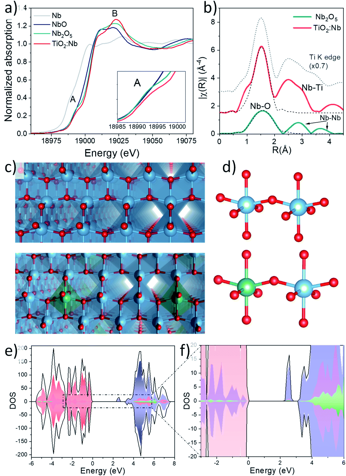 | ||
| Fig. 2 (a) XANES spectra at the Nb K-edge for Nb2O5 and Nb-doped TiO2 thin-films together with Nb metal foil and NbO references. (b) Fourier transform moduli (solid line) and fit (dashed line) of EXAFS spectra at the Nb K-edge for Nb-doped TiO2 thin films and the N2O5 reference. (c) Models of the crystal lattice and (d) unit cell of bare and Nb doped anatase TiO2. Atom colours: Ti (blue), O (red), Nb (green). (e and f) Density of states (DOS) of Nb-doped anatase. Total DOS profiles (black), O 2p (red), Ti 3d (blue), and Nb 5d (green). | ||
The simulated spectrum presents great similarities with the measured spectrum and further suggests the incorporation of Nb5+ ions into the anatase structure where Nb5+ ions replace Ti4+ ions as substitutional dopants. On the other hand, the Ti K edge XANES spectra exhibit clear changes in the intensity and shape of the A2 and A3 features of Nb doped samples which are associated with a partial reduction of Ti4+ ions to accommodate Nb5+ species in the structure (more details in section S5 and Fig. S8a†). Extended X-ray absorption fine structure (EXAFS) fitting of the first shell performed at the Nb K-edge for Nb2O5 and Nb-doped TiO2 and Ti K-edge in Nb doped TiO2 is depicted in Fig. 2b and S8b† respectively. Considering the lower signal to noise ratio for the EXAFS region of the doping element, Fourier transform (FT) was performed in a reduced k-range: 3–10 Å−1 and higher shells are less resolved. Therefore, only a fitting of the first shell was carried out and the results of this fit are summarized in Table S2† in the ESI. The FT of the EXAFS signal at the Ti K-edge in this reduced k-range is also shown for comparison.
For the Nb doped TiO2 sample, Nb5+ ions present an octahedral coordination and the bond distance is 2.00(2) Å, in perfect agreement with the distance reported by other authors for Nb-doped TiO2.41 Another interesting feature is the similarity of the second shell at the Ti and Nb K-edge, which suggests the presence of a Ti second shell around the Nb cations, further confirming the presence of Nb5+ ions in the anatase structure (compare with the dotted grey line representing EXAFS of the Ti K-edge). In contrast, the coordination number of Nb cations in Nb2O5 was fixed to 5 for a good fit, in agreement with the results reported by other authors,42,43 and the quite high value of the σ2 parameter reflects a high bond-distance dispersion, which can be attributed to the presence of four longer Nb–O bonds (∼2.06 Å) and one shorter Nb![[double bond, length as m-dash]](https://www.rsc.org/images/entities/char_e001.gif) O bond (1.82 Å). In our case no improvement in the fit was obtained considering the model with two different sub-shells. Two Nb–Nb coordination shells are also observed at longer distances (∼2.7 and 3.7 Å on the phase uncorrected scale) in the Nb2O5 samples.
O bond (1.82 Å). In our case no improvement in the fit was obtained considering the model with two different sub-shells. Two Nb–Nb coordination shells are also observed at longer distances (∼2.7 and 3.7 Å on the phase uncorrected scale) in the Nb2O5 samples.
DFT calculations for the Nb–TiO2 doped system were carried out to determine the changes in the structural and electronic properties. First, to determine the relative stability of Nb doped TiO2, the substitution energy (Es) was calculated, considering that four Ti atoms are replaced, using eqn (1):
| Es = ENbTiO2 + 4ETi − 4ENb − EbTiO2 | (1) |
| ENbfm = ENbTiO2 − 68ETi − 144EO − Ed | (2) |
The HSE06 density of states (DOS) analyses were carried out on Nb-doped TiO2 (NbxTi1−xO2) (Fig. 2e and f). The valence band (VB) is mainly constituted by the overlapping of O 2p and Ti 3d orbitals, while the conduction band minimum (CBM) is primarily formed by Ti 3d orbitals. In addition, a narrow peak in the band gap, centred at 0.6 eV below the conduction band minimum is observed, exhibiting a strongly localised charge density on a single Ti site in a nearest-neighbour position relative to the Nb dopant. Small contributions of neighbouring O atoms and Nb atoms, proportional to their concentration, were also observed. Previous investigations using the DFT+U approach attribute the presence of an intra band gap peak to a Ti-centered small polaron, resulting in a partial reduction of Ti atoms (Ti3+)47 which play a crucial role in the electronic conductivity enhancement, allowing a rapid electron replacement and reducing the probability of trapping electrons from the CB.48
Electrochemical performance analysis by XPS and in situ XAS
Once the substitutional nature of the Nb5+ doping within the synthesised anatase NCs and the effects on its structure were confirmed, we proceeded to analyse the electrochemical effects of this substitution by XPS and in situ XAS experiments.A set of cyclic voltammetry experiments at different scan rates was performed to investigate the electrochemical behaviour of the system under study (Fig. S10†). A Li-based electrolyte was used to investigate both surface and bulk charge processes. At low scan rates, the voltammetry shows a similar capacity between bare and doped samples. However, at high scan rates, an increase in the system load is observed in the Nb-doped sample. It is well known that the effects related to surface charge are more noticeable at high scan rate analysis.25,49 A possibility is to attribute this overall charge capacitance effect to the surface effect associated with the presence of LSPRs in the doped NCs, something we will address later. Moreover, looking at the CVs in detail (inset graphs Fig. S11†), even at low scan rates, a change in the shape of the CV of the Nb-doped sample also suggests an increase in the current at lower potentials.
The origin of the charge capacitance differences between these systems could be found through the analysis of the evolution of the chemical environment of the Ti and Nb atoms within the bare and doped samples.
First, we performed XPS studies of samples before and after electrochemical reduction. By quantification of the Ti 2p and Nb 3d regions we estimate a Nb doping of 13% for both pristine and reduced samples. Compared with the bulk Nb/Ti ratio (9.8% according to ICP studies), we observe a partial surface segregation, which has been previously reported.23 This experiment also shows that the reduction–oxidation cycles do not lead to further Nb phase segregation.
Fig. 3 displays the XPS spectra of a Nb:TiO sample in the Ti 2p and Nb 3d regions before and after the reduction processes. The spectrum of the as-prepared sample features intense peaks in the Ti 2p and Nb 3d regions with maxima at 459.5 eV and 207.7 eV, which are well within the expected binding energy range for Ti(IV) and Nb(V) cations, respectively. After the sample has been subjected to reducing chronoamperometric conditions (−1.9 V vs. Ag/Ag+), two important changes can be observed in the spectrum: (i) new low binding energy components emerge both in the Ti 2p and the Nb 3d regions and (ii) there is a shift of the whole spectrum (observed on both core lines) toward higher binding energy by about 0.3 eV. The chemical shift of the emerging components in the Ti 2p (which is 2.5 eV off the main Ti4+ component) and Nb 3d (which is 1.6 eV off the main Nb5+ component) regions can be associated with the presence of Ti3+ and Nb4+ cations, which suggests that both the host Ti and dopant Nb are reduced during the electrochemical reaction.
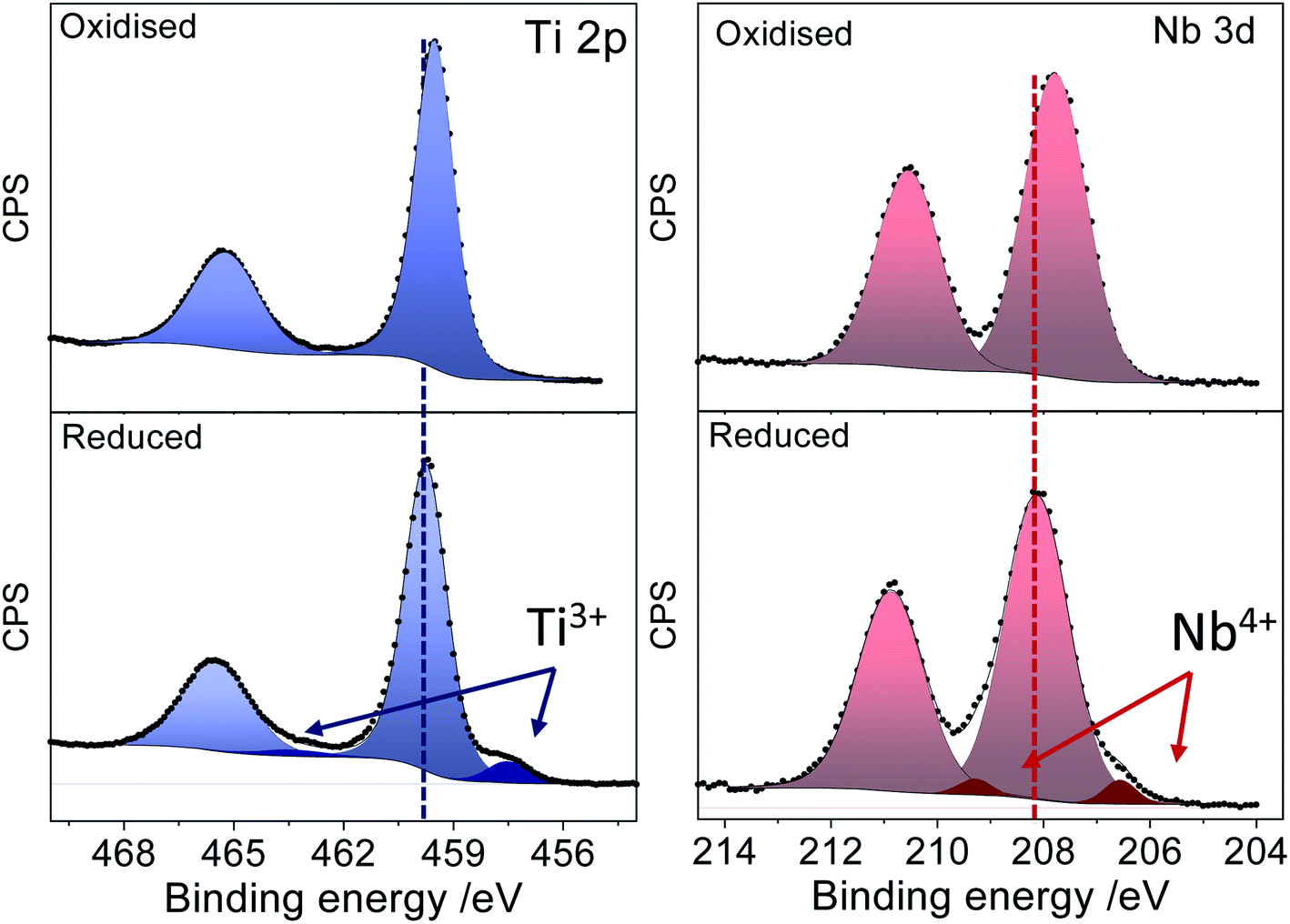 | ||
| Fig. 3 XPS spectra of oxidised (upper panel) and reduced (lower panel) Nb doped TiO2 in the Ti 2p and Nb 3d regions. | ||
Ti3+ and Nb4+ introduce electron density donor states, leading to an effective n-type doping of the system that pins the Fermi level further into the conduction band. Since all spectra are referenced to the Fermi level, this results in the observed shift of the spectrum of the reduced sample to a higher binding energy (BE). This observation also suggests that the reduction of the cations does not lead to a segregation of reduced phases. Instead the reduced species remain within the anatase structure, bringing about the observed electronic modulations to the whole system.
XPS postmortem analyses show that the electrochemical reduction of the Nb doped TiO2 sample involves the reduction of both the Ti and Nb cations within the network, at least at the surface of the sample. In order to study what is actually happening during the electrochemical reduction of the material, we carried out the in situ XAS experiment. In situ XAS was used to investigate the polaron absorption effect responsible for the visible electrochromic phenomena and to study key differences between bare and Nb doped TiO2 under smart window operation conditions. In this way, in situ XAS measurements were performed at both Ti and Nb K-edges. Fig. 4a and b show the cyclic voltammograms at 20 mV s−1 of both systems and the potential values where the in situ XAS experiment was performed. The samples were measured under open circuit potential (OCP) conditions (Fig. 4 lighter spheres) and under reduction conditions (Fig. 4 dark spheres) to finally return to the OCP and study the reversibility of the system (oxidised samples). Fig. 4c shows the XANES spectra at the Ti K-edge for the Nb-doped TiO2 sample measured at OCP and reduction potentials while the inset shows the spectra of bare TiO2 under the same conditions. Remarkable differences are observed in both samples during the reduction reaction with a clear change in the spectral features compared to the samples measured under OCP conditions. The absorption edge shifts towards lower energies and the pre-edge region also suffers noticeable changes. Two well defined resonances, 4987 and 5001 eV, appear on the white line at the reduction potential and there is a slight decrease in the absorption intensity at around 4970 eV, in correspondence with the A2 feature (see Fig. 2 and S8† in the ESI for comparison). All these results indicate a partial reduction of Ti4+ to Ti3+ ions. These results are in agreement with previously reported studies,18,50 where these spectral modifications induced at the Ti K-edge during reduction are clear evidence of Li-ion intercalation in the anatase structure and the well-known transition from a tetragonal phase towards a distorted orthorhombic LiXTiO2 phase:30,51,52
| TiO2 + xLi+ + xe− ⇌ LixTiO2; x < 0.5 | (3) |
 | ||
| Fig. 4 Cyclic voltammograms of (a) Nb doped TiO2 and (b) bare TiO2 at 20 mV s−1 in 1 M LiClO4 in propylene carbonate. The lighter spheres represent the point where the measurement was carried out before reducing the materials (OCP) and the darker is the point at which the spectra called Red_TiO2 and Red_TiO2:Nb were recorded. (c) XANES spectra at the Ti K-edge for Nb-doped TiO2 thin films at OCP and reduction potential. The spectrum of undoped TiO2 is also shown for comparison (dotted line). The inset shows the XANES spectra of undoped TiO2 at oxidation and reduction potential. (d) XANES spectra at the Nb K-edge for Nb-doped TiO2 thin films at oxidation and reduction potentials. The spectrum of Nb2O5 at reduction potential is also shown for comparison (dotted line). The inset shows the XANES spectra of Nb2O5 at oxidation and reduction potentials. | ||
The obtained spectra were similar for the bare and Nb-doped samples at the reduction potential (see Fig. 4c, main spectra and inset). However, the Nb-doped TiO2 sample shows tiny but noticeabe differences in the XANES spectra, such as: (i) a slightly lower absorption of the pre-edge peaks at around 4970 eV; (ii) a lower absorption of the resonance at 5001 eV. These spectral differences reveal an improvement in the electrochemical reduction reaction provoked by the substitution of Ti4+ by Nb5+ ions in anatase TiO2.
The average oxidation state after reduction of Ti ions was estimated using an integral method similar to what was reported before53 and using Ti metal, Ti2O3 and TiO2 as references with known oxidation states (Fig. S12† in the ESI). The oxidation state calculated for bare and Nb-doped TiO2 is around 3.6 and 3.5, respectively, suggesting that on Li+ ion intercalation, X in eqn (3) is 0.4 in the Nb doped sample and 0.5 in the bare one. Therefore, a slightly higher reduction of Ti ions is detected in the Nb-doped sample revealing a more efficient reduction process. Besides, the measured spectra at OCP and oxidation potentials after the reduction process (Fig. S13† in the ESI) are practically equal, thus revealing a great reversibility of the system after the electrochemical reduction.
Fig. S14† in the ESI shows the FT moduli of the EXAFS spectra of undoped and Nb-doped TiO2 samples measured at the Ti K-edge under reduction and OCP conditions. After the reduction, the first coordination shell is made of a mixture of Ti4+ and Ti3+ (confirmed by the XANES) bonded to oxygen in octahedral coordination and the Ti–O bond distance increases from 1.956(6) Å to 1.98(1) (TiO2) and 2.01(1) Å (TiO2:Nb), (see Table S5†). The lengthening of the Ti–O bond distance reflects the increased ionic size of Ti3+ ions (67 pm) compared to Ti4+ (60 pm) in octahedral coordination.54 The longer Ti–O bond distance observed for the Nb-doped sample suggests that the amount of Ti3+ ions formed under the reduction conditions is slightly higher compared to the undoped TiO2 and agrees with the analysis of the average oxidation state of Ti ions. The small differences observed in the XANES features, such as a lower absorption in the pre-edge region (4968–4974 eV) and the lower intensity of the white line resonance at 5001 eV (Fig. 3) also indicate a higher amount of Ti3+ formed in the Nb-doped sample. The increased Ti–O bond distance causes a smaller overlap of Ti 3d and O 2p orbitals and this causes a shift of the A2 pre-peak of the XANES region towards lower energy, as reported before.50 For the Nb-doped sample there is also a higher local disorder around Ti4+/Ti3+ ions, as confirmed from the higher Debye–Waller parameters (Table S5, ESI†). Another interesting difference at the reduction potential is the remarkable intensity decrease of the coordination shells at longer distances (2.5–3.5 Å on the phase-uncorrected scale), where the Ti–Ti coordination shells of the anatase structure appear. This confirms the occurrence of a phase transition during the intercalation of Li+ ions and confirms the formation of a LiXTiO2 phase, as suggested by the XANES spectra, with a corresponding decrease of Ti–Ti coordination shells.
XANES spectra under reduction and OCP conditions were also recorded at the Nb K-edge for Nb2O5 and the Nb-doped TiO2 sample. In this experiment, we observe a very interesting phenomenon, which was never investigated before under in situ conditions to the best of our knowledge. Tiny changes are observed for the Nb2O5 sample during reduction, (inset of Fig. 3d), while remarkable changes are observed for the Nb-doped TiO2 sample, confirming the XPS analysis explained before. The absorption edge of Nb-doped TiO2 shifts by 2.6 eV towards lower energy and the appearance of two resonances at around 19010 and 19020 eV are distinctive features of the formation of Nb4+ species in the form of NbO2.55 This different electrochemical activity of Nb ions in Nb2O5 and TiO2 is another clear indication of the presence of Nb ions in the anatase structure more than the as isolated Nb2O5 domains. Besides, in light of these results, Nb5+ is significantly more reduced as a dopant within TiO2 than in Nb2O5 oxide.
The FT moduli of the EXAFS signals together with the first shell fit for the Nb-doped TiO2 sample at OCP and reduction potential are shown in Fig. S15† in the ESI. The results of the fit clearly indicate the formation of Nb4+ species during reduction where Nb4+ ions are in octahedral coordination and the Nb–O bond distance increases to ∼2.09(2) Å (Table S6†) in rough agreement with the bond distance of NbO2 reported by other authors.56 Despite the first shell in NbO2 being made of a distorted octahedron, here only a single Nb–O bond distance was considered due to the limited k-range available (k ∼ 10 Å−1). The σ2 parameter is quite large and this reflects the distorted octahedral structure obtained during reduction conditions. After the oxidation reaction, the Nb4+ ions are oxidized again to Nb5+ and the Nb–O decreases to 1.99 Å, similar to what was found for the ex-situ results of Nb doped TiO2 (Table S6†).
In summary, this exhaustive study reveals the fascinating role of the dopant under smart window operation conditions. We have discovered that Nb not only modifies the electronic structure of anatase, but is also active in the reduction process, observing substantial changes in the reduction of Nb5+ to Nb4+ during the electrochemical process. Moreover, the inclusion of Nb allows a more effective reduction of the Ti within the doped anatase.
This ability of the doped material to be reduced more effectively could be the basis of the improved charge capacitance in the electrochemical reduction performance of the Nb-doped TiO2 compared with the bare one and can be related to the better electronic conductivity calculated using DFT and previously reported data,49 faster lithium ion diffusivity,25 and higher surface charge of the Nb doped TiO2 NCs. Furthermore, based on previous calculations of the intercalation energy of lithium in these systems,57 Nb-doped TiO2 has a lower intercalation energy than pristine TiO2 anatase, revealing that Nb-doping induces a relatively more stable structure for lithium intercalation. Additionally, due to their high surface area to volume ratio, small NCs provide a higher proportion of electrically charged species closer to the surface (compared to bulk materials) and can aid in faster ion/electron transfer processes. This may facilitate charge storage in the electrodes through surface effects only exhibited by Nb doped TiO2.
In situ spectroelectrochemistry and electrochemical impedance spectroscopy
Once the highest accumulated capacitance associated with Li+ intercalation and therefore with the polaronic absorption of the doped system was determined, the dual band behaviour at different applied potentials of this material was investigated by combining electrochemical impedance spectroscopy (EIS) with in situ spectroelectrochemistry. To perform this study, EIS was carried out along a wide electrochemical window to understand the changes in the electrical properties induced by the dopant with the applied potential.58 Besides, a smart window lab-scale device with high transparency was assembled (Fig. S19†) to explore the spectroelectrochemical changes at equivalent potentials.Fig. 5a shows the Nyquist plots obtained at the reduction potential at which in situ XAS was performed (−1.9 V Ag/Ag+), where two arcs can be distinguished. Additionally, Fig. S16† shows the Nyquist plots at other measured potentials, showing a reduction in the arc with the cathodic applied bias. Due to the porous nature of the fabricated films and the presence of two arcs in the Nyquist plots, an equivalent circuit composed of two RC couples in parallel is employed, considering both the ITO/electrolyte and the TiO2/electrolyte interfaces.59 The employed equivalent circuit is shown in the inset of Fig. S16.† At first glance, Nb doping reduces the series resistance in good agreement with previous studies.49,60 Additionally, a reduction in the charge transfer resistance was also measured for the whole potential window by the addition of Nb to the TiO2 host lattice. Fig. S17a† shows the acquired series and charge transfer resistance of the analysed samples at different scan potentials. On the other hand, Fig. 5b shows the extracted capacitance from the EIS measurements at different applied potentials together with the cyclic voltammetry (CV) curves of the analysed samples.
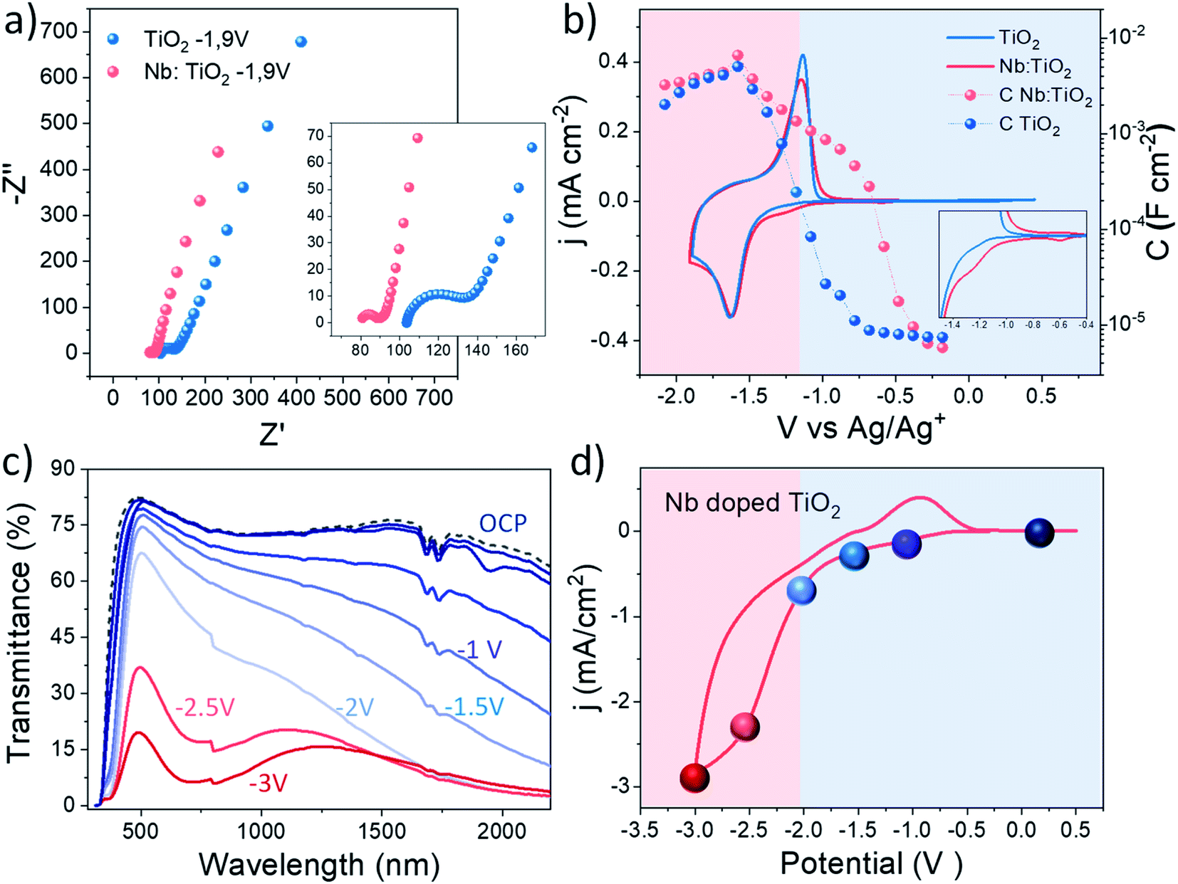 | ||
| Fig. 5 (a) Nyquist Plot of bare and Nb doped TiO2 at −1.9 V vs. Ag/Ag+. (b) Cyclic voltammetry (solid lines) and charge capacitance (balls) associated with the different potential points of TiO2 (blue) and Nb-doped TiO2 (red). (c) Transmittance spectra and (d) cyclic voltammogram of a lab-scale device of Nb doped TiO2 at 50 mV s−1. The spheres represent the potential points at which the transmittance measurements of the device have been carried out. | ||
The extracted capacitance from the ITO/electrolyte interface is shown in Fig. S18,† where a flat behaviour of the capacitance typical of a double layer capacitance is observed along the whole potential window.61 The capacitance of both samples was calculated in the same potential range as the voltammetry (Fig. 5b) showing a peak at around −1.6 V vs. Ag/Ag+, perfectly matching the reduction wave observed in the cyclic voltammetry, related to the Li+ intercalation within the bulk of the films.15,62 The maximum value of the capacitance is very similar in both samples as shown by the similar shape observed in the voltammograms, being slightly higher in Nb:TiO2, especially at higher cathodic bias, matching the results observed by in situ XAS experiments. Furthermore, the Nb doped sample shows a much earlier onset in the capacitance than the bare TiO2 sample, as will be further discussed below. Additionally, the charge transfer resistance (Rct) of the analysed samples (Fig. S18a†) shows a decrease with the cathodic applied potential, as expected. The Nb doped sample exhibits a slightly lower resistance than bare TiO2 along the whole potential window, more likely attributed to the enhanced conductivity induced by the dopant.
On the other hand, the density of states (DOS) of the conduction band (CB) of the analysed samples was extracted from the capacitance through the expression C = e × DOS.63 The obtained shape of the DOS of the CB (Fig. S17b†) is in good agreement with that in previous studies.64,65 As can be observed, the Nb doped sample shows a slightly higher value of the peak at around 5 eV, meaning a slight increase in the electron density at the conduction band minimum, which has been previously reported for Nb doped TiO2.15
To correlate these results with the dual band functionality of this material, in situ spectroelectrochemical experiments were performed. Fig. 5c and d show the transmittance spectra and cyclic voltammograms of the lab-scale smart window device, respectively. The colored spheres in the cyclic voltammograms represent the potential points at which the spectroelectrochemical measurements were performed. Under the application of a moderate voltage, and previously to the peak that represents the Li+ intercalation in the device (blue spheres), a modulation in the optical transmittance in the NIR range is observed, which can be attributed to the surface plasmon absorption. At these voltages (0 to −2 V), the Li+ ions did not intercalate deeply into TiO2, but instead accumulated around the NC surface to balance the higher electron concentration of the semiconductor. On the other hand, the reddish spheres in Fig. 5d represent the potentials at which the intercalation of lithium and therefore the reduction of the electrode, begin to appear. In this potential range (−2.5 and −3 V), the optical transmittance reduction in the VIS range begins to decrease, as an effect of the intense polaron absorption associated with the massive insertion of Li+ ions occurs at these potentials within the TiO2 host lattice. See in Fig. S20† images of the lab scale smart window device under operation conditions.
In light of these results, it is possible to attribute the early increase in the extracted capacitance of the Nb doped TiO2 to the presence of the LSPR phenomenon. Hence, two different potential regions can be distinguished in the doped sample: (i) between 0 and −2 V: this region is governed by the LSPR phenomenon, observed by the enhanced transmittance at these potentials and an early onset in the extracted capacitance (reddish region in Fig. 5b). (ii) At potentials between −2.5 and −3.5 V, the polaron absorption governs the reduction in the transmittance, as a consequence of the bulk Li intercalation, and this is reflected in the increase in the capacitance matching the reduction wave in the CV (blueish region in Fig. 5b).
Conclusions
Pristine and Nb-doped anatase nanocrystals with an average size of 5 nm have been successfully synthesized and the two electrochromic modes (polaronic and plasmonic absorption) have been observed and characterised. An in-depth analysis of the behaviour of these materials in both modes has been carried out, finding relevant information that helps elucidate their performance in smart window devices. In relation to the polaronic absorption responsible for the optical changes in the visible part, an exhaustive in situ X-ray absorption spectroscopy study was carried out. The study reveals the more effective reduction of Ti within the doped anatase material and a substantial reduction of Nb5+ to Nb4+ during the electrochemical process, much larger than the structural changes observed for Nb5+ within the lattice of its own oxide (Nb2O5). This first time analysis of the dopant's edge during operation conditions expose the active role of Nb not only in modifying the electronic structure of the host oxide, but also playing an active role in the reduction process.The observed improvement in the electrochemical reduction process when Ti4+ atoms are replaced by Nb5+ can be attributed to the better electronic conductivity and higher lithium intercalation observed by EIS, as well as a superior ability to store charge through surface reactions/effects, thanks to the higher surface/volume ratio in this system due to the change in crystalline size domains.
The polaron and plasmon absorptions present in these doped NCs were investigated through a combination of EIS measurements and in situ spectroelectrochemistry. As far as we know, the dual effect of Nb doping has been directly observed in the extracted capacitance from EIS for the first time in this work. In the potential region where lithium intercalation and therefore polaronic absorption occur, a slight increase in the capacitance of the doped material was observed, in good agreement with in situ XAS experiments. An early increase in the extracted capacitance of Nb doped TiO2 was observed at lower applied potentials that can be attributed to the LSPR exhibited by these NCs.
The combined application of in situ electrochemical XAS, XPS analysis, in situ spectroelectrochemistry and EIS has allowed us to unravel the polaron and plasmon absorption phenomena exhibited in Nb doped anatase NCs, that are the basis of the excellent performances as smart window materials. This strategy could be used to unveil the behavior of other doped NCs that exhibit this fascinating dual band behavior and are pivotal for applications such as batteries, supercapacitors and smart windows.
Conflicts of interest
The authors declare no conflict of interest.Acknowledgements
This work was supported by the national projects NovaCO2 (PID2020-118593RB-C22) and Nhympha (PID2019-106315RB-I00) funded by MCIN/AEI/10.13039/501100011033 and the regional project FotoArt-CM (S2018/NMT-4367) funded by Comunidad de Madrid. M. B. thanks the Spanish MICINN the Juan de la Cierva Incorporación grant (IJC2019 – 042430 –I). Ex situ and in situ XAS experiments were performed at the CLAESS beamline of the ALBA synchrotron (proposal number AV-2020074403) with the support of the ALBA staff. The researchers would like to thank Dr Fernando Picó for his valuable help in acquiring FESEM and AFM images and the X-ray diffractograms and Iván García Dominguez and Francisco Martínez López, floor coordinators at ALBA Synchrotron, for their help with the design and 3D printing of the electrochemical cell used for in situ X-ray absorption measurements.References
- S. K. Deb, Sol. Energy Mater. Sol. Cells, 2008, 92, 245–258 CrossRef CAS.
- D. T. Gillaspie, R. C. Tenent and A. C. Dillon, J. Mater. Chem., 2010, 20, 9585–9592 RSC.
- L. Belussi, B. Barozzi, A. Bellazzi, L. Danza, A. Devitofrancesco, C. Fanciulli, M. Ghellere, G. Guazzi, I. Meroni, F. Salamone, F. Scamoni and C. Scrosati, J. Build. Eng., 2019, 25, 100772 CrossRef.
- L. Neij, S. Sandin, M. Benner, M. Johansson and P. Mickwitz, Energy Res. Social Sci., 2021, 72, 101864 CrossRef.
- X. Cao, X. Dai and J. Liu, Energy Build., 2016, 128, 198–213 CrossRef.
- N. DeForest, A. Shehabi, S. Selkowitz and D. J. Milliron, Appl. Energy, 2017, 192, 95–109 CrossRef.
- C. G. Granqvist, İ. Bayrak Pehlivan and G. A. Niklasson, Surf. Coat. Technol., 2018, 336, 133–138 CrossRef CAS.
- K. Wang, Q. Meng, Q. Wang, W. Zhang, J. Guo, S. Cao, A. Y. Elezzabi, W. W. Yu, L. Liu and H. Li, Advanced Energy and Sustainability Research, 2021, 2, 2100117 CrossRef.
- C. A. Gueymard, Sol. Energy, 2004, 76, 423–453 CrossRef.
- E. L. Runnerstrom, A. Llordés, S. D. Lounis and D. J. Milliron, Chem. Commun., 2014, 50, 10555–10572 RSC.
- S. Cao, S. Zhang, T. Zhang, Q. Yao and J. Y. Lee, Joule, 2019, 3, 1152–1162 CrossRef CAS.
- S. L. Gibbs, C. Dean, J. Saad, B. Tandon, C. M. Staller, A. Agrawal and D. J. Milliron, Nano Lett., 2020, 20, 7498–7505 CrossRef CAS PubMed.
- M. Barawi, G. Veramonti, M. Epifani, R. Giannuzzi, T. Sibillano, C. Giannini, A. Rougier and M. Manca, J. Mater. Chem. A, 2018, 6, 10201–10205 RSC.
- S. Cao, S. Zhang, T. Zhang and J. Y. Lee, Chem. Mater., 2018, 30, 4838–4846 CrossRef CAS.
- M. Barawi, L. De Trizio, R. Giannuzzi, G. Veramonti, L. Manna and M. Manca, ACS Nano, 2017, 11, 3576–3584 CrossRef CAS PubMed.
- H. Gu, C. Guo, S. Zhang, L. Bi, T. Li, T. Sun and S. Liu, ACS Nano, 2018, 12, 559–567 CrossRef CAS PubMed.
- J. Kim, G. K. Ong, Y. Wang, G. LeBlanc, T. E. Williams, T. M. Mattox, B. A. Helms and D. J. Milliron, Nano Lett., 2015, 15, 5574–5579 CrossRef CAS PubMed.
- C. J. Dahlman, Y. Tan, M. A. Marcus and D. J. Milliron, J. Am. Chem. Soc., 2015, 137, 9160–9166 CrossRef CAS PubMed.
- G. A. Niklasson, L. Berggren and A.-L. Larsson, Sol. Energy Mater. Sol. Cells, 2004, 84, 315–328 CrossRef CAS.
- C. G. Granqvist, Thin Solid Films, 2014, 564, 1–38 CrossRef CAS.
- V. G. Kravets, A. V. Kabashin, W. L. Barnes and A. N. Grigorenko, Chem. Rev., 2018, 118, 5912–5951 CrossRef CAS PubMed.
- A. Agrawal, S. H. Cho, O. Zandi, S. Ghosh, R. W. Johns and D. J. Milliron, Chem. Rev., 2018, 118(6), 3121–3207 CrossRef CAS PubMed.
- O. Nicoletti, F. de la Peña, R. K. Leary, D. J. Holland, C. Ducati and P. A. Midgley, Nature, 2013, 502, 80–84 CrossRef CAS PubMed.
- A. Llordés, G. Garcia, J. Gazquez and D. J. Milliron, Nature, 2013, 500, 323–326 CrossRef PubMed.
- M. Lübke, J. Shin, P. Marchand, D. Brett, P. Shearing, Z. Liu and J. A. Darr, J. Mater. Chem. A, 2015, 3, 22908–22914 RSC.
- Y. Wang, B. M. Smarsly and I. Djerdj, Chem. Mater., 2010, 22, 6624–6631 CrossRef CAS.
- S. A. Ansari, M. M. Khan, M. O. Ansari and M. H. Cho, New J. Chem., 2016, 40, 3000–3009 RSC.
- M. D. Calisir, M. Gungor, A. Demir, A. Kilic and M. M. Khan, Ceram. Int., 2020, 46, 16743–16753 CrossRef CAS.
- S. Lee, J. H. Noh, H. S. Han, D. K. Yim, D. H. Kim, J.-K. Lee, J. Y. Kim, H. S. Jung and K. S. Hong, J. Phys. Chem. C, 2009, 113, 6878–6882 CrossRef CAS.
- M. Wagemaker, D. Lützenkirchen-Hecht, A. A. van Well and R. Frahm, J. Phys. Chem. B, 2004, 108, 12456–12464 CrossRef CAS.
- D. Deng, M. G. Kim, J. Y. Lee and J. Cho, Energy Environ. Sci., 2009, 2, 818–837 RSC.
- L. R. Sheppard, T. Bak and J. Nowotny, J. Phys. Chem. B, 2006, 110, 22447–22454 CrossRef CAS PubMed.
- J. Yue, C. Suchomski, P. Voepel, R. Ellinghaus, M. Rohnke, T. Leichtweiss, M. T. Elm and B. M. Smarsly, J. Mater. Chem. A, 2017, 5, 1978–1988 RSC.
- M. Fehse, S. Cavaliere, P. E. Lippens, I. Savych, A. Iadecola, L. Monconduit, D. J. Jones, J. Rozière, F. Fischer, C. Tessier and L. Stievano, J. Phys. Chem. C, 2013, 117, 13827–13835 CrossRef CAS.
- L. De Trizio, R. Buonsanti, A. M. Schimpf, A. Llordes, D. R. Gamelin, R. Simonutti and D. J. Milliron, Chem. Mater., 2013, 25, 3383–3390 CrossRef CAS.
- Z. Yang, D. Choi, S. Kerisit, K. M. Rosso, D. Wang, J. Zhang, G. Graff and J. Liu, J. Power Sources, 2009, 192, 588–598 CrossRef CAS.
- R. Giannuzzi, R. D. Silva, M. Barawi, L. D. Trizio, G. Veramonti, A. Qualtieri, L. Manna and M. Manca, ECS Trans., 2017, 77, 1671 CrossRef CAS.
- T. Brezesinski, J. Wang, J. Polleux, B. Dunn and S. H. Tolbert, J. Am. Chem. Soc., 2009, 131, 1802–1809 CrossRef CAS PubMed.
- P. C. Angelomé, L. Andrini, M. E. Calvo, F. G. Requejo, S. A. Bilmes and G. J. A. A. Soler-Illia, J. Phys. Chem. C, 2007, 111, 10886–10893 CrossRef.
- F. Fresno, D. Tudela, J. M. Coronado, M. Fernández-García, A. B. Hungría and J. Soria, Phys. Chem. Chem. Phys., 2006, 8, 2421–2430 Search PubMed.
- D. S. Bhachu, S. Sathasivam, G. Sankar, D. O. Scanlon, G. Cibin, C. J. Carmalt, I. P. Parkin, G. W. Watson, S. M. Bawaked, A. Y. Obaid, S. Al-Thabaiti and S. N. Basahel, Adv. Funct. Mater., 2014, 24, 5075–5085 CrossRef CAS.
- C. Tiozzo, C. Bisio, F. Carniato, A. Gallo, S. L. Scott, R. Psaro and M. Guidotti, Phys. Chem. Chem. Phys., 2013, 15, 13354–13362 RSC.
- H. Yoshida, T. Tanaka, T. Yoshida, T. Funabiki and S. Yoshida, Catal. Today, 1996, 28, 79–89 CrossRef CAS.
- J. Liu, M. Weng, S. Li, X. Chen, J. Cen, J. Jie, W. Xiao, J. Zheng and F. Pan, Phys. Chem. Chem. Phys., 2019, 22, 39–53 RSC.
- F. Zhao, B. Wang, Y. Tang, H. Ge, Z. Huang and H. K. Liu, J. Mater. Chem. A, 2015, 3, 22969–22974 RSC.
- L. E. Depero, L. Sangaletti, B. Allieri, E. Bontempi, R. Salari, M. Zocchi, C. Casale and M. Notaro, J. Mater. Res., 1998, 13, 1644–1649 CrossRef CAS.
- B. J. Morgan, D. O. Scanlon and G. W. Watson, J. Mater. Chem., 2009, 19, 5175–5178 RSC.
- H. Usui, S. Yoshioka, K. Wasada, M. Shimizu and H. Sakaguchi, ACS Appl. Mater. Interfaces, 2015, 7, 6567–6573 CrossRef CAS PubMed.
- C. Cavallo, G. Calcagno, R. P. de Carvalho, M. Sadd, B. Gonano, C. M. Araujo, A. E. C. Palmqvist and A. Matic, ACS Appl. Energy Mater., 2021, 4, 215–225 CrossRef CAS.
- M. Wagemaker, G. J. Kearley, A. A. van Well, H. Mutka and F. M. Mulder, J. Am. Chem. Soc., 2003, 125, 840–848 CrossRef CAS PubMed.
- R. J. Cava, D. W. Murphy, S. Zahurak, A. Santoro and R. S. Roth, J. Solid State Chem., 1984, 53, 64–75 CrossRef CAS.
- M. Wagemaker, W. J. H. Borghols and F. M. Mulder, J. Am. Chem. Soc., 2007, 129, 4323–4327 CrossRef CAS PubMed.
- J. Timoshenko and B. Roldan Cuenya, Chem. Rev., 2021, 121, 882–961 CrossRef CAS PubMed.
- R. D. Shannon, Acta Crystallogr., Sect. A: Cryst. Phys., Diffr., Theor. Gen. Crystallogr., 1976, 32, 751–767 Search PubMed.
- C.-S. Huang, C.-L. Huang, Y. Liu, S. Lin, T.-S. Chan and H.-W. Tu, Chem. Mater., 2018, 30, 1769–1775 CrossRef CAS.
- C. Sanloup, B. Cochain, C. de Grouchy, K. Glazyrin, Z. Konôpkova, H.-P. Liermann, I. Kantor, R. Torchio, O. Mathon and T. Irifune, J. Phys.: Condens. Matter, 2018, 30, 084004 CrossRef CAS PubMed.
- S.-N. Kao, Y.-C. Hung, Y. Shimoyama, C.-M. Hsieh and B. K. Chang, J. Taiwan Inst. Chem. Eng., 2021, 125, 314–322 CrossRef CAS.
- M. N. Shaddad, D. Cardenas-Morcoso, M. García-Tecedor, F. Fabregat-Santiago, J. Bisquert, A. M. Al-Mayouf and S. Gimenez, ACS Omega, 2019, 4, 16095–16102 CrossRef CAS PubMed.
- B. Klahr, S. Gimenez, F. Fabregat-Santiago, J. Bisquert and T. W. Hamann, J. Am. Chem. Soc., 2012, 134, 16693–16700 CrossRef CAS PubMed.
- H. Bae, J.-S. Ha, S. Park, T. Chikyow, J. Chang and D. Oh, J. Vac. Sci. Technol., B: Nanotechnol. Microelectron.: Mater., Process., Meas., Phenom., 2012, 30, 050603 Search PubMed.
- F. Fabregat-Santiago, G. Garcia-Belmonte, J. Bisquert, P. Bogdanoff and A. Zaban, J. Electrochem. Soc., 2003, 150, E293 CrossRef CAS.
- S. Y. Huang, L. Kavan, I. Exnar and M. Grätzel, J. Electrochem. Soc., 1995, 142, L142–L144 CrossRef CAS.
- S. Corby, M.-G. Tecedor, S. Tengeler, C. Steinert, B. Moss, C. A. Mesa, H. F. Heiba, A. A. Wilson, B. Kaiser, W. Jaegermann, L. Francàs, S. Gimenez and J. R. Durrant, Sustainable Energy Fuels, 2020, 4, 5024–5030 RSC.
- M. Quesada-Gonzalez, B. A. D. Williamson, C. Sotelo-Vazquez, A. Kafizas, N. D. Boscher, R. Quesada-Cabrera, D. O. Scanlon, C. J. Carmalt and I. P. Parkin, J. Phys. Chem. C, 2018, 122, 714–726 CrossRef CAS.
- D. O. Scanlon, C. W. Dunnill, J. Buckeridge, S. A. Shevlin, A. J. Logsdail, S. M. Woodley, C. R. A. Catlow, M. J. Powell, R. G. Palgrave, I. P. Parkin, G. W. Watson, T. W. Keal, P. Sherwood, A. Walsh and A. A. Sokol, Nat. Mater., 2013, 12, 798–801 CrossRef CAS PubMed.
Footnote |
| † Electronic supplementary information (ESI) available. See https://doi.org/10.1039/d2ta03239b |
| This journal is © The Royal Society of Chemistry 2022 |