
 Open Access Article
 This Open Access Article is licensed under a Creative Commons Attribution-Non Commercial 3.0 Unported Licence
Insight into the preponderant role of the lattice size in Sn-based colusites for promoting a high power factor†
Paulina
Kamińska
 ab,
Cédric
Bourgès
*be,
Raju
Chetty
b,
Daniel
Gutiérrez-Del-Río
b,
Piotr
Śpiewak
a,
Wojciech
Święszkowski
a,
Toshiyuki
Nishimura
c and
Takao
Mori
*bd
ab,
Cédric
Bourgès
*be,
Raju
Chetty
b,
Daniel
Gutiérrez-Del-Río
b,
Piotr
Śpiewak
a,
Wojciech
Święszkowski
a,
Toshiyuki
Nishimura
c and
Takao
Mori
*bd
aMaterials Design Division, Faculty of Materials Science and Engineering, Warsaw University of Technology, Wołoska 141, 02-507 Warsaw, Poland
bWPI International Center for Materials Nanoarchitechtonics (WPI-MANA), National Institute for Materials Science (NIMS), Namiki 1-1, Tsukuba, 305-0044, Japan. E-mail: BOURGES.Cedric@nims.go.jp; MORI.Takao@nims.go.jp
cResearch Center for Structural Materials, National Institute for Materials Science (NIMS), Namiki 1-1, Tsukuba, 305-0044, Japan
dGraduate School of Pure and Applied Sciences, Tsukuba University, Tennoudai 1-1-1, Tsukuba 305-8671, Japan
eInternational Center for Young Scientists (ICYS), National Institute for Materials Science, Namiki 1-1, Tsukuba, Ibaraki 305-0044, Japan
First published on 8th April 2022
Abstract
We investigated the feasibility of the co-doping effect of zinc and chromium for copper and vanadium substitution, respectively, and reported the first successful Cr incorporation within the bulk Sn-based colusite structure. We demonstrated that this could be achieved by combining process and lattice engineering to open a small solubility window within this sterically restricted V site. The thermoelectric properties of the colusite Cu25ZnV2−xCrxSn6S32 (x = 0–0.5) have been examined on sintered ingots over the temperature range of 300–700 K. As a result, we achieved the highest average power factor ever reported for Sn-based colusites. For the first time, our findings point out a striking insight related to the lattice size effect and its contribution to the Seebeck coefficient of Sn-based colusites. All the experimental results were rationalized by theoretical calculations. Using this unique finding, we finally optimized the compound by hot-pressing treatment and reported a competitive zT value of 0.8 at 700 K for the sample Cu25ZnV1.75Cr0.25Sn6S32.
1. Introduction
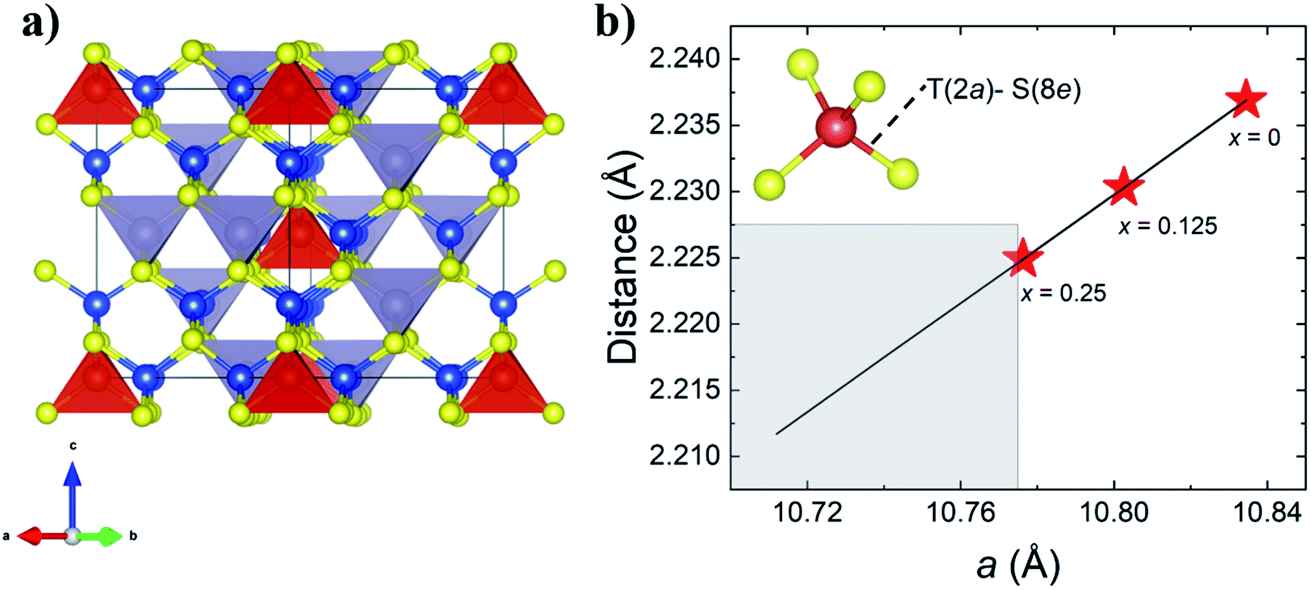
The thermoelectric (TE) effect allows us to directly and reversibly convert waste heat to electrical energy making it one of the possible spearhead technologies towards carbon neutrality, by usefully harvesting the large amount of available waste heat in current society.1–4 The conversion efficiency of a TE device depends on the dimensionless thermoelectric figure of merit zT, described as follows: zT = S2T/ρκ, where T stands for absolute temperature, S is the Seebeck coefficient, ρ is the electrical resistivity, and κ is the total thermal conductivity. κ is the sum of electronic (κel) and lattice (κlat) contributions i.e., κ = κel + κlat. Nowadays, most of the TE materials presenting large zT values (i.e. Bi2Te3,5,6 PbTe,7,8 GeTe,9,10 and PbSe11), benchmarked in the range of unity, are composed of either toxic or rare elements, such as Bi, Pb, Ge, Se, or Te. To address this issue, several classes of low-cost and/or earth-abundant TE materials have been investigated over the last few decades, e.g., oxides, sulfides, and Heusler-based compounds.12Among the newly discovered classes of sustainable TE materials, Cu-based sulfides have been drawing scientists' attention due to their intrinsic advantages: promising TE performance and consisting of cost-effective, low density, earth-abundant, and less-toxic constituent elements.13 The group of auspicious materials includes both natural minerals and synthetic derivatives from ternary to quaternary compounds such as Cu2−xS,14–17 bornite Cu5FeS4,18–21 chalcopyrite CuFeS2,22–28 Cu-based thiospinels,29–32 Cu4Sn7S16,33,34 kesterite-type and derivatives Cu2TrMsS4 (Tr = Fe, Co, Ni, Zn, Ms = Ge, Sn),35–39 tetrahedrites Cu12−xTMxSb4S13 (TM = Mn, Fe, Co, Ni, Zn),40–46 and the materials currently in focus colusites Cu26T2M6S32 (T = V, Nb, Ta, Cr, Mo, W, Ti; M = Ge, Sn, Sb).47–49
The colusite compound family has been extensively investigated within the last 8 years for its promising performance, currently achieving the symbolic unity value of zT, ranking it as one of the best TE sulfide materials. Among the preliminary steps to achieve this good performance, the major roles of the synthesis approaches,48,50,51 pristine composition,47,52–54 doping,50,55–58 and defect chemistry48,54,59 have been reported and systematically correlated to their influences on the intrinsic crystal, electronic and vibrational structures of the material. This deep understanding of the structure/property relationship in the colusite structure-type enabled the possibility of controlling its native versatile transport properties and building a pathway towards the application stage. Indeed, a recent report about the Cu26Cr2Ge6S32 colusite revealed an exceptionally high power factor close to 2 mW m−1 K−2 as well as a zT value close to unity at 700 K, which is comparable to those of the current conventional TE materials.53 They showed that an introduction of hexavalent T6+ cations (T = Cr, Mo, W) leads to interactions between them and the conductive “Cu–S” network, which can be successfully used to tune the electronic transport properties. Recently, a scalable synthesis for industrial production as well as a remarkable thermal stability at high temperatures have been reported, which can pave the way for the social implementation of colusite-based TE materials.60–62 It is worth mentioning that a first prototype colusite-based thermoelectric power generation module has already been successfully developed with a conversion efficiency of η ≈ 5.5%, and with a temperature difference (ΔT) of 390 K.63
Nevertheless, even though colusites with attractive thermoelectric properties have already been achieved thanks to the Cr effect, Ge-based colusites partially step aside from the native cost-efficiency interest of the material by containing 10 at% of highly expensive Ge instead of Sn at the 6c tetrahedral site. So far, there are no reports on the successful incorporation of Cr within Sn-based colusites. Besides, several murky areas remain in the possible intrinsic contribution of the structural features to the transport properties, especially the amplitude variation of the Seebeck coefficient, which needs to be unraveled to achieve the full potential of the structural type.
For instance, co-doping is a promising strategy to effectively tune the structural features and improve the electronic and thermal properties. Previously, this strategy has been successfully applied to several groups of materials reported in the literature.35,64–67 Herein, we investigated the synergic effect of the two dopants that have provided the best results so far – Zn and Cr. We demonstrated that it is necessary to use co-doping in order to open a small solubility window of Cr within a sterically restricted V site, and highlighted the role of the structural lattice. We performed the synthesis of dense samples of Cu25ZnV2−xCrxSn6S32 (x = 0, 0.125, 0.25, 0.375, 0.5) and characterized the thermoelectric properties in the temperature range from 300 K to 700 K. The experimental results were rationalized with ab initio calculations to sustain the experimental interpretation.
2. Experimental and theoretical sections
2.1. Sample preparation
So far, two common approaches have been used in the literature to successfully obtain a colusite structure: (i) synthesis by direct reaction of the elements and annealing in evacuated quartz tubes,47 and (ii) synthesis by using mechanical alloying.50 In the present work, a combined synthesis method was employed – samples of Cu25ZnV2−xCrxSn6S32 (0 ≤ x ≤ 0.5) were prepared by direct reaction of the elements, followed by annealing and a ball-milling process. Stoichiometric quantities of elements Cu (Sigma Aldrich, ≥99.99%, 2–8 mm beads), V (Alfa Aesar, 99.7% pieces), Cr (Aldrich, 99.9995%, chips), Sn (High Purity Materials, 99.999%, 2–3 mm pieces), and S (Sigma Aldrich, ≥99.99%, flakes) were sealed in an evacuated quartz tube. All the samples were heated to 673 K, kept at this temperature for 2 h, and then heated to the synthesis temperature – 1373 K. After being kept for 50 h, they were cooled down to 1073 K and annealed for another 50 h to improve their homogeneity. All heating and cooling rates were set at ∼100 K h−1. The obtained powders were then milled in a mixer (SPEX 8000M Mixer/Mill) for 2 hours under an argon atmosphere. This process was crucial to obtain single-phase compounds with good mechanical properties. The ground powders were sieved down to <90 μm and were then densified by spark plasma sintering (SPS-1080 – SPS Syntec Inc.) at 873 K for 30 min under a uniaxial pressure of 50 MPa (heating and cooling rate of 50 K min−1 and 25 K min−1, respectively). Selected compounds were also densified by using a hot-press (FVHP-I-3, Fujidempa Kogyo Co., Ltd, Osaka, Japan) at 923 K for 15 min. The geometrical densities range from 90% to 99% of the theoretical values for the SPS sintered samples and from 95 to 99% for the hot-pressed samples. The sintered pellets were then cut and polished into the required shapes and dimensions for various measurements.2.2. Characterization
The crystal structures of the sintered pellets were examined using X-ray powder diffraction (Rigaku Smart Lab 3 diffractometer) with Cu-Kα radiation. Data were collected over a 2θ range of 10–100° with a step size of 0.02° and a step time of 2° min−1.Le Bail fittings were performed using the FullProf program included in the WinPLOTR software.68–70 The shape of the diffraction peaks was modeled using a pseudo-Voigt profile function. Zero-point shift, asymmetry parameters, and lattice parameters were systematically refined, and the background contribution was manually estimated.
Observations of the microstructural aspects of the sintered samples were performed on the fractured cross-section and polished surface using a Hitachi SU-4800 scanning electron microscope (SEM) and a mini-SEM (TM3000, Hitachi), both equipped with an energy-dispersive spectrometer (EDS).
The measurements of electrical resistivity ρ and Seebeck coefficient S were performed simultaneously using a commercial Ulvac ZEM-2 instrument under partial helium pressure. The thermal diffusivity α was measured using an LFA-467 Hyperflash (Netzsch) under a flowing nitrogen atmosphere (50 ml min−1). The thermal conductivity κ = D × CP × d was calculated as a product of the geometrical density of sample d, thermal diffusivity D, and theoretical heat capacity Cp from the Dulong–Petit approximation (CP = 3R, where R is the real gas constant). The lattice thermal conductivity κlat was calculated by subtracting the electronic contribution κel according to the Wiedemann–Franz law (κel = LTρ−1). L is the Lorenz number derived from the following equation: L = 1.5 + exp[−|S|/116] based on a single parabolic band model with acoustic phonon scattering.71
2.3. Band structure calculations
The electronic band structures and density of states (DOS) of Cu26V2Sn6S32, Cu25ZnV2Sn6S32, and Cu25ZnCr0.5V1.5Sn6S32 have been calculated within the Perdew–Burke–Ernzerhof (PBE) generalized gradient approximation (GGA). All calculations were performed with projector augmented wave (PAW) pseudopotentials generated by Kresse and Joubert72,73 implemented in the Vienna ab initio simulation package (VASP) code.74 The plane-wave cut-off energy was set to 400 eV. A 66-atom unit cell (as shown in Fig. 4a) has been used for pristine and Zn-doped samples. We adopted a k-point grid of 5 × 5 × 5 mesh integrated with the tetrahedron method with Blöchl corrections. Investigation of the effect of different arrangements of the Zn and Cu ions showed that such disordering does not significantly affect the electronic properties of the studied systems. Therefore, we chose the Zn atom to replace Cu on the 6d site, as this system exhibits slightly lower energy than two other possible systems (that is, Zn on 8e and 12f sites). Then calculations were performed for different chromium positions in relation to other elements. Two compositions, x = 0 and x = 0.5, were selected for the calculations. For the composition x = 0.5, a cell consisting of 132 atoms was used. All the structures were relaxed until the forces on the atoms were less than 0.01 eV Å−1. Because of the presence of localized 3d-electrons, calculations were conducted with the simplified Dudarev approach with Ueff = U − J = 3.5 eV for Cu and V 3d orbitals, 12.0 eV for Zn 3d orbitals, and 2.5 eV for Cr 3d orbitals.45 Theoretical predictions of the Seebeck coefficient for pristine colusites were calculated employing the semi-classical Boltzmann transport equation (BTE) within the constant scattering time approximation, as implemented in the BoltzWann code.75 In order to achieve reasonable transport properties a dense k-point mesh of 40 × 40 × 40 was used to compute the transport properties. | ||
| Fig. 1 Electronic density of states (DOS) for Cu26V2Sn6S32, Cu25ZnV2Sn6S32, and Cu25ZnCr0.5V1.5Sn6S32. | ||
 | ||
| Fig. 2 Electronic density of states (DOS) for Cu26V2Sn6S32 assuming different lattice parameters a (10.74 Å, 10.82 Å, and 10.90 Å). | ||
 | ||
| Fig. 3 (a) Powder X-ray diffraction patterns of sintered Cu25ZnV2−xCrxSn6S32 compounds by SPS and 440 peaks in the expanded scale, (b) evolution of the unit cell parameter with the Cr content and (c) BSE-SEM analysis results on the polished surface of the Cu25ZnV1.75Cr0.25Sn6S32 sample sintered by SPS with the corresponding EDS mapping. | ||
 | ||
| Fig. 4 (a) Schematic representation of the Cu26T2Sn6S32 crystal structure (b) theoretical T(2a)–S(8e) interatomic distance dependence on the lattice parameter. Red stars indicate the data of current study samples. The grey square indicates the lattice parameter range wherein the structure cannot accommodate Cr substitution. | ||
3. Results and discussion
3.1 Density functional theory calculations
Fig. 1 shows the density of states of reference Cu26V2Sn6S32 and single/co-doped Cu25ZnV2−xCrxSn6S32 (x = 0, 0.5). For all the samples, the valence band maximum (VBM) consists of hybridized Cu-3d and S-3p orbitals, where the EF lies inside the valence band with unoccupied states (or holes), which is responsible for the p-type metallic conduction character of the material. This finding is in line with previous reports.47 The DOS for all samples showed a sharp peak close to the top of the valence band (≈−0.2 eV), indicating a high density of states near the EF.
The VBM exhibits a multivalley character with large effective masses (Fig. S1†). The conduction band minimum (CBM) for x = 0 comprises the V-3d and S-3p orbitals. On the other hand, for x = 0.5, new impurity bands can be noticed in the bandgap around 0.5 eV above the EF. These additional bands are mainly composed of Cr-3d and S-3p orbitals, thus independent of the spin polarization. It was observed that transition metal (TM) substitution created hybridized impurity levels both within the valence bands and in the bandgap, thereby modifying the band structure and altering the band degeneracy near EF, which is otherwise highest for the pristine compound.47,48 We obtained no magnetic moment in the ground state of the calculated lattice which sustains a valence state of Cr6+ within the colusite structure.
Table 1 shows the estimated p values for the pristine compound and the samples Cu25ZnV2−xCrxSn6S32 (x = 0, 0.5). The charge carrier concentration is evaluated for samples Cu26V2Sn6S32 and the single/co-doped Cu25ZnV2−xCrxSn6S32 (x = 0, 0.5) using the following equation:76
 | (1) |
 | (2) |
| Cu26−δZnδV2−xCrxSn6S32 | |||||
|---|---|---|---|---|---|
| @300K | μ (eV) | p (1021 cm−3) | m*/me | p (1021 cm−3) (DFT) | m*/me (DFT) |
| δ = 0 x = 0 (i S = 90 μV K−1) | 2.8 | 2.7 | 11.6 | 2.92 | 9.4 |
| δ = 0 x = 0 (ii S = 125 μV K−1) | 1.7 | 2.7 | 8.5 | ||
| δ = 1 x = 0 (S = 168 μV K−1) | 0.75 | 1.0 | 9.7 | 2.3 | 8.8 |
| δ = 1 x = 0.5 (S = 49 μV K−1) | 5.3 | 1.6 | 3.5 | 1.6 | 3.1 |
The reduced chemical potential (μ) is estimated from the measured Seebeck coefficient value at 300 K using a single parabolic band assumption:77
 | (3) |
 | (4) |
To gain more insight into the S, we computed the effective mass (m*) using the following expression:
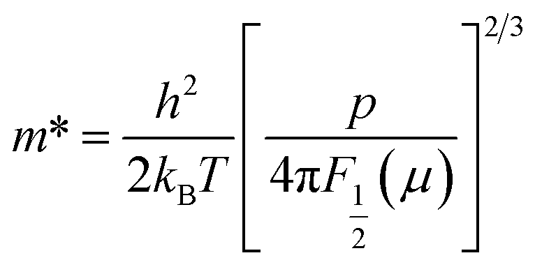 | (5) |
The p value decreased from ∼2.7 × 1021 cm−3 for Cu26V2Sn6S32 to 1.0 × 1021 cm−3 for Cu25ZnV2Sn6S32, which is because of the substitution of Zn on the Cu site that reduced the number of charge carriers (holes). Further, the p value increased to ∼1.6 × 1021 cm−3 for Cu25ZnCr0.5V1.5Sn6S32. This trend is in good agreement with the experimental results (cf. part 3.4) showing a decrease in ρ and S with the increase of Cr content in Cu25ZnV2−xCrxSn6S32. The determined m* values are shown in Table 1. m* ∼3.5m0 is obtained for Cu25ZnCr0.5V1.5Sn6S32, which is almost three times lower than m* ∼9.7m0 for Cu25ZnV2Sn6S32. This result indicates that a higher charge carrier mobility is expected for the Cr substituted samples. Besides, the effective mass was also calculated using the band curvature (eqn (6)) to confirm the computed results, which is in agreement with the m* values obtained from the measured S values (Table 1).
 | (6) |
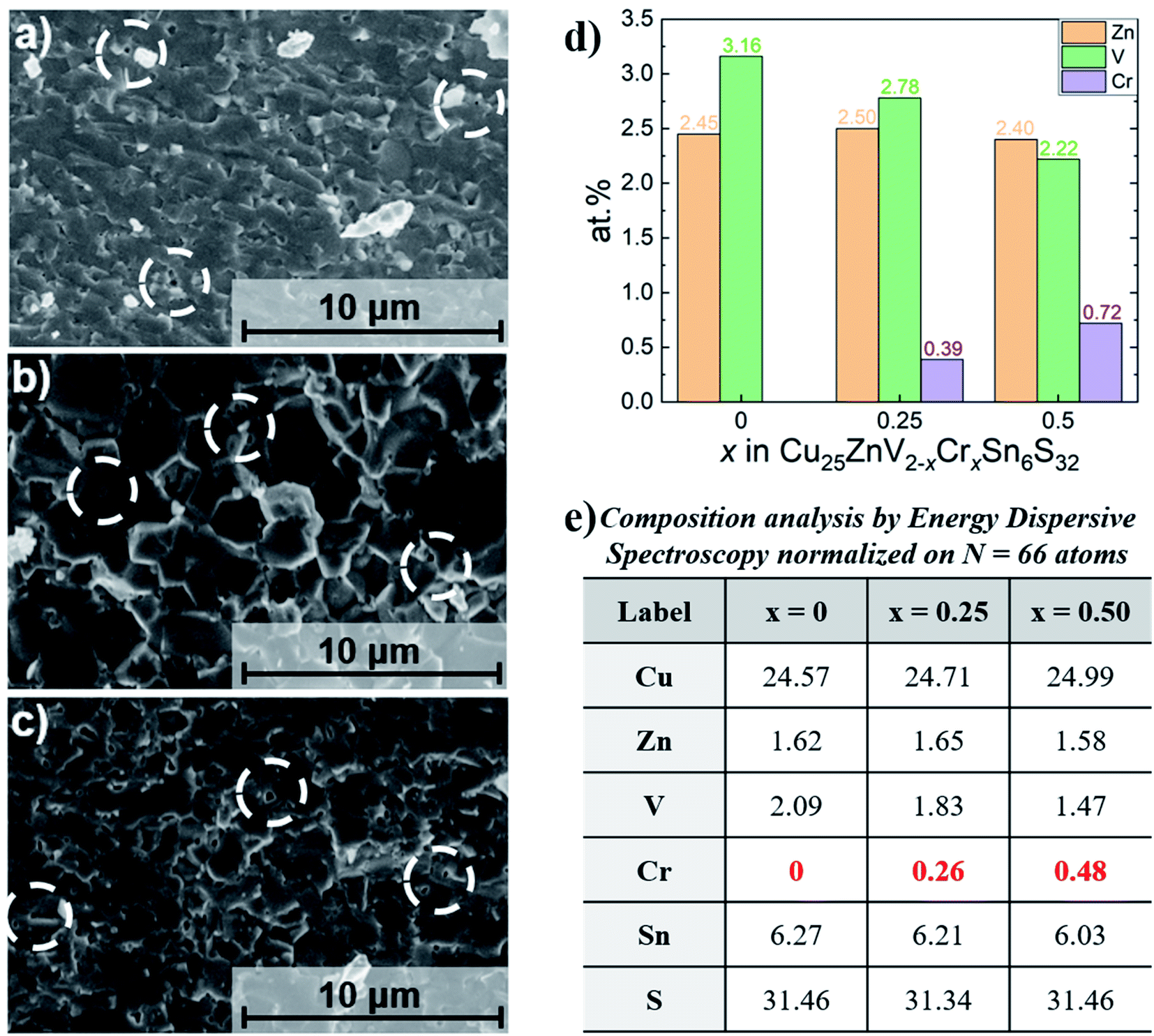 | ||
| Fig. 5 SEM images of a fractured surface of Cu25ZnV2−xCrxSn6S32 (a) x = 0, (b) x = 0.25, (c) x = 0.5, (d) and (e) corresponding composition analysis by EDS. | ||
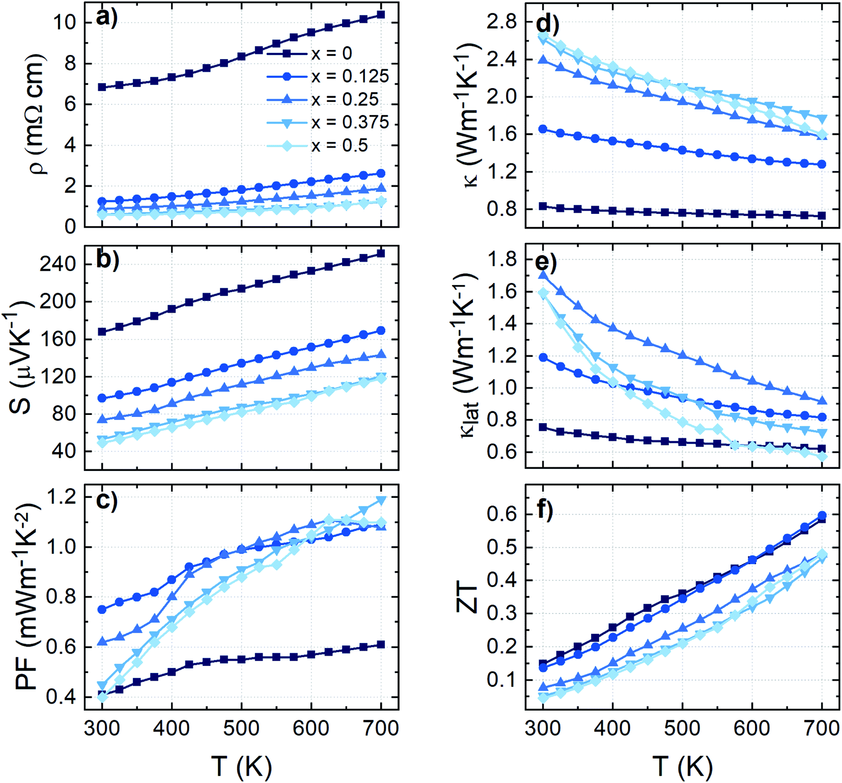 | ||
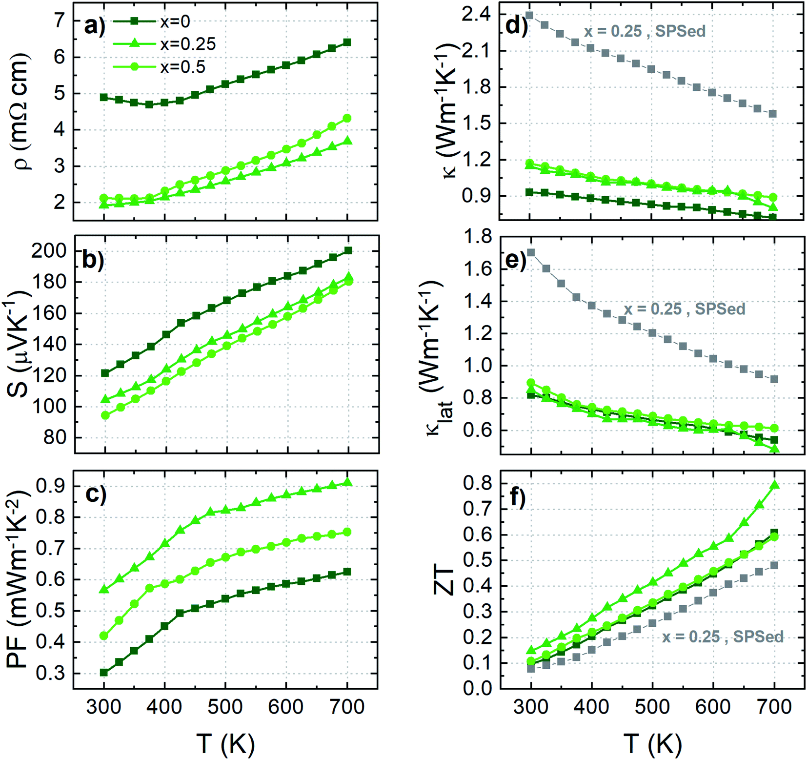
| Fig. 6 Temperature dependence of (a) electrical resistivity ρ, (b) Seebeck coefficient S, (c) thermal conductivity κ, (d) lattice thermal conductivity κlat, (e) power factor PF, and (f) dimensionless thermoelectric figure of merit zT for colusite Cu25ZnV2−xCrxSn6S32. | ||
 | ||
| Fig. 7 (a) Plot of the Seebeck coefficient at room temperature versus the corresponding lattice parameter of Sn-based colusites reported in the literature data from ref. 47, 48, 50–52, 55, and 59–61 (b) Pisarenko plot of the Seebeck coefficient dependence on the charge carrier concentration for different lattice sizes. | ||
As a result of our theoretical investigation, we revealed that a larger lattice negligibly creates a carrier concentration change in the Sn-colusite (Table 2) but, interestingly, will contribute to a larger effective mass for a defined composition and therefore lead to a superior Seebeck coefficient independent of the carrier concentration range.
| a (Å) | p (1021 cm−3) | m*/m0 |
|---|---|---|
| 10.74 | 2.92 | 9.4 |
| 10.82 | 2.90 | 11.9 |
| 10.90 | 2.78 | 12.5 |
This latter feature is illustrated by the dependence of the Seebeck coefficient, calculated at room temperature, on the carrier concentration for different lattice sizes (Fig. 7b) which confirmed the observation and is discussed further with the experimental data in part 3.4.
3.2 Structural analysis
The samples were synthesized by direct reaction of the elements and annealing, followed by ball milling to reduce the grain size. Subsequent to ball milling, powder X-ray diffraction (PXRD) was performed to investigate the influence of the ball-milling time. It was found that a ball-milling treatment exceeding 2 hours has not changed the PXRD pattern (Fig. S3†) but resulted in a fine powder distribution. Consequently, it strengthens the final mechanical properties of the pellet after the sintering step as discussed in a later part.The room temperature PXRD patterns of sintered colusites Cu25ZnV2−xCrxSn6S32 are shown in Fig. 3a. The prominent diffraction peak positions and intensities agree with the theoretical colusite cubic structure (space group no. 218, P![[4 with combining macron]](https://www.rsc.org/images/entities/char_0034_0304.gif) 3n; a ≈ 10.7 Å). With the increasing x content of Cr, we can observe peaks shifting to higher angles, characteristic of the decreasing lattice parameter (Fig. 3 and 4b). This was also confirmed through the Le Bail refinement of the lattice parameter (Fig. 3b). The decreasing lattice parameters are coherent with the aimed substitution of the V by the Cr according to their theoretical ionic radii, respectively VIV5+ = 0.355 Å and CrIV6+ = 0.26 Å or/and possibly CrIV5+ = 0.345 Å.78 In the previous report of Pavan Kumar et al., the authors demonstrated, through the combination of XRD and neutron analysis, that Cr will favorably be in the valence state 6+.53 This is consistent with our theoretical calculations (part 3.1) suggesting that no magnetic moment induced by Cr on the doped sample agrees with the absence of an unpaired electron in Cr6+. Furthermore, the substitution of Cr on the V site was corroborated by energy dispersive spectroscopy (EDS) (Fig. 5d and e and S4–S6†). It is worthy to point-out that the too close energy between the Kβ(V) and Kα(Cr) peaks (highlighted in the Fig. S4b–S6b and S9b–S11b†) makes it impossible to differenciate the position of the V and Cr on the EDS mapping. However, Kα(V) is independent of the Cr wavelength which makes it possible to quantitatively estimate the amount of Cr, thanks to the variation of the intensity ratio
3n; a ≈ 10.7 Å). With the increasing x content of Cr, we can observe peaks shifting to higher angles, characteristic of the decreasing lattice parameter (Fig. 3 and 4b). This was also confirmed through the Le Bail refinement of the lattice parameter (Fig. 3b). The decreasing lattice parameters are coherent with the aimed substitution of the V by the Cr according to their theoretical ionic radii, respectively VIV5+ = 0.355 Å and CrIV6+ = 0.26 Å or/and possibly CrIV5+ = 0.345 Å.78 In the previous report of Pavan Kumar et al., the authors demonstrated, through the combination of XRD and neutron analysis, that Cr will favorably be in the valence state 6+.53 This is consistent with our theoretical calculations (part 3.1) suggesting that no magnetic moment induced by Cr on the doped sample agrees with the absence of an unpaired electron in Cr6+. Furthermore, the substitution of Cr on the V site was corroborated by energy dispersive spectroscopy (EDS) (Fig. 5d and e and S4–S6†). It is worthy to point-out that the too close energy between the Kβ(V) and Kα(Cr) peaks (highlighted in the Fig. S4b–S6b and S9b–S11b†) makes it impossible to differenciate the position of the V and Cr on the EDS mapping. However, Kα(V) is independent of the Cr wavelength which makes it possible to quantitatively estimate the amount of Cr, thanks to the variation of the intensity ratio 
We can notice that the exsolution process, usually observed in Sn-based colusites, has been avoided by partially substituting Cu with a small amount of Zn.50,57 For the sample x ≥ 0.25, we can observe an additional low-intensity diffraction peak appearing at 2θ ≈ 29.1° belonging to the covellite CuS phase (space group no. 194, P63/mmc, a ≈ 3.757 Å c ≈ 16.19 Å), attesting to the apparent solubility limit of the Cr substitution in the V site. These results are coherent with the EDS mapping analysis (Fig. 3c and S5–S6†) which evidences the presence of the secondary phase, even in the x = 0.25 sample only visible in the back scattered electron (BSE) image due to the sub-micron range of the precipitates (Fig. 3c).
An in-depth investigation highlighted that Cr substitution in Sn-based colusite was achievable due to the steric effect induced by the co-substitution with Zn, associated with the native off-stoichiometry originating from the sealed tube synthesis. Sn-based colusites are characterized by a weaker capacity to accommodate their structure than the Ge-based ones, and this is the origin of several intrinsic physicochemical features such as: (i) the exsolution process cited above, (ii) relatively poor mechanical properties, and, in the present case, (iii) the difficulty to perform substitution with small elements such as Cr. The Sn atomic radius (0.55 Å), being far larger than Ge (0.39 Å), results in Sn-based colusites having a steric restriction. In the present case, Zn-doping drives an expansion of the Sn-based colusites' lattice, as extensively reported in the literature.50,55,79 In addition, the synthesis process using conventional sealed tube synthesis favours a cationic-rich composition filling the E site and promotes a lattice dilation compared to the mechanical alloying process.59 An interatomic distance T(2a)–S(8e) ≈ 2.228 Å is reported experimentally in the Ge-based colusite, for full Cr occupancy within the T site.53,58Fig. 4b shows the simulation of the interatomic distance T(2a)–S(8e) (T(2a): V/Cr site) dependence on the lattice parameter. It is stressed that structural widening is crucial for respecting the interatomic distance and consequently achieving Cr substitution in the Sn-based colusites. In our case, a large lattice parameter of a = 10.834 Å for the pristine sample opened a window of interatomic distances in agreement with a corresponding theoretical T(2a)–S(8e) interatomic distance of 2.237 Å. That minimal distance is respected down to a ≈ 10.77–10.78 Å, with a corresponding interatomic distance in the range of that of the Ge-based colusite and experimentally confirmed by our samples as shown by the red stars in Fig. 4b. Below that critical lattice parameter, Cr-substitution cannot be accommodated by the Sn-based structure, which explains the secondary phase's favourable formation and the lattice parameter's saturation for the sample with x ≥ 0.25 (Fig. 3b).
3.3 Scanning electron microscopy
Considering the previous report on Zn-doping and the significant effect of the process on the microstructure of colusite, all the samples have been screened by scanning electron microscopy (SEM) to confirm the influence of co-substitution and the combined synthesis process on the microstructure of the current samples.Fig. 5a–c show the SEM images of the fractured Cu25ZnV2−xCrxSn6S32 (x = 0, 0.25, 0.5). All samples showed a similar microstructure regardless of the Cr content. The preliminary samples developed without a ball-milling step were characterized by large grains with irregular shapes (Fig. S7†), leading to a systematic transgranular cleavage and fracture, thus preventing the possibility of performing further property characterization studies. The ball milling process was found necessary to promote a reduced grain size in the range of a few micrometers, with a fine angular grain shape. The reasonable mechanical strength observed in our samples has its origin in this specific ball-milled microstructure. According to the Hall–Petch relation, the yield stress ε scales with the inverse square root of the grain size δ in polycrystalline materials according to the following relation:
| ε = ε0 + k/√δ | (7) |
All samples are characterized by the presence of intergranular nanoporosities distributed homogeneously within the matrix, especially in the Cr-doped samples. It can be expected that the existence of nanoporosities would not significantly affect the carrier mean free path and, therefore, the electrical conductivity. However, it has not been excluded that it might enhance the phonon scattering in the samples, as discussed in a later section.
3.4 Thermoelectric properties
The thermoelectric properties of Cu25ZnV2−xCrxSn6S32 (x = 0–0.5) compounds from 300 to 700 K are shown in Fig. 6. All the samples showed a positive Seebeck coefficient (S) that confirms that the major carriers are holes. The positive temperature dependency of electrical resistivity (ρ) indicates the metal-like behavior for all the samples. This result is in good agreement with the band structure calculations (Fig. 1 and S1†) as the Fermi level for all the compounds lies within the valence band.For the pristine sample (x = 0), the electrical resistivity (ρ) varies from 6.8 to 10.4 mΩ cm and the S increases from 168 to 252 μV K−1, respectively at 300 K and 700 K, leading to the maximum power factor, PF (= S2/ρ), of 0.6 mW m−1 K−2 at 700 K. These values are in fair agreement with similar colusites synthesized by the direct reaction method reported by Suekuni et al.47,56 However, it should be noted that the measured S values are much higher than the S values (= 65–145 μV K−1 at 300 to 700 K) of the same composition (Cu25ZnV2Sn6S32) synthesized by mechanical alloying despite a close stoichiometry.50 The main observable difference is that our present Zn-doped colusite has an apparently larger lattice (a = 10.835 Å) than the ball-milling one (a ≈ 10.767 Å), which suggests a relationship between the Seebeck coefficient and the colusite lattice.
For samples x > 0, a significant drop of the ρ is observed in the whole temperature range with increasing Cr content. For example, the ρ decreases from 7 mΩ cm for x = 0 to 0.5–1.5 mΩ cm for x > 0 at 300 K (Fig. 6a). Pavan Kumar et al. presented the concept of a conductive ‘Cu–S’ network as an ion sublattice that dominates the electronic states active in transport. The interstitial T cations, forming mixed tetrahedral–octahedral [TS4]Cu6 complexes, induce distortions and introduce ionic scattering channels in the conductive ‘Cu–S’ network. However, unlike many other reported T6+ cations, chromium, thanks to its smaller size and lower electronegativity, leads to strong T–Cu interactions without significantly perturbing the conductive network, thus leading to a drastic reduction in ρ, which is consistent with our results (Fig. 6a).58 Simultaneously, the S decreased with increasing Cr content. For example, the S values decrease from 100 to 60 μV K−1 at 300 K, and from 170 to 150 μV K−1 at 700 K for x = 0.125 and 0.5, respectively (Fig. 6b). For x ≥ 0.25, it can be noted that there is no significant variation of S values, which is in good agreement with the PXRD results confirming the solubility limit of the Cr in the matrix. Moreover, it can be noted that the secondary phase, namely CuS, does not seem to have a major impact on the electrical transport as expected.30
The Seebeck coefficient of a degenerate semiconductor is directly proportional to m* and inversely proportional to n2/3 according to Mott's formula, which is expressed as:
 | (8) |
The initial band structure calculations, discussed in the theoretical part (Fig. 1 and S1†), revealed that Cr substitution slightly raises the hole concentration, which is consistent with the experimentally observed decrease of the S. However, the measured S value dramatically falls from ≈160 μV K−1 to ≈50 μV K−1, respectively for x = 0 and x = 0.5 at room temperature. The reference (Cu26V2Sn6S32 with a = 10.74 Å) sample Pisarenko plot (Fig. 7b) suggests that the carrier concentration shift should be in the range of an order of magnitude (p ≈ 1 × 1020 cm−3 to ≈3 × 1021 cm−3 respectively for S ≈ 160 μV K−1 and ≈50 μV K−1). This increase appears far from the theoretical estimation of the carrier concentration variation induced by Cr doping previously calculated (Table 1). Hall measurements were attempted to determine the charge carrier concentration in the pristine and doped samples to evidence the carrier concentration trend. Unfortunately, the attempted measurements remained unsuccessful, most likely attributed to the low carrier mobility.
To understand the large variation of the S, an in-depth investigation and analysis of the relationship of S with the respective lattice size for Sn-based colusite has been performed in an intensive literature survey. Indeed, the lattice ranges in colusite are broad and likely vary from a ≈ 10.74–10.90 Å.47,48,50–52,55,59–61 Such dilatation/contraction of the lattice can be first provided by the substitution/doping of an impurity element like, for example, Cr in the present study. However, in sulphide-based materials, a certain flexibility in the lattice is also commonly observed which is mainly related to the sulfur off-stoichiometry unavoidable in most of the process approaches due to the high vapour pressure of the sulphur element. This will lead to a slight composition deviation with a cation-rich ratio due to the sulphur deficiency in the case of a higher annealing/sintering temperature process. It will make the formation of interstitial cations within the structure or a different cationic distribution within the crystallographic sites propitious. For example in the Sn-based colusite, it is reported that Cu can favourably occupy the interstitial sites 6b (0, 0, 0.5) and/or 24i (≈0.25, ≈0.25, ≈0) and that Sn can form SnCu antisite defects.52,59,81 In both cases, it will induce a lattice variation despite an apparently similar composition. Fig. 7a shows the resulting plot of the Seebeck coefficient versus the corresponding lattice parameter for all the Sn-based colusites reported in the literature including the present work. It demonstrates an apparent pseudo-linear dependency between the S and the corresponding lattice size of the Sn-based colusite in the range of a ≈ 10.73–10.85 Å. The evident tendency to promote a globally larger Seebeck coefficient for a larger lattice parameter and the reverse is highlighted, regardless of the composition/doping or synthesis approach. Indeed, the lattice size modifies the Sn-colusite band structure near the Fermi level, as we described in the theoretical part (cf. part 3.1). The DOS peak near the Fermi level appears sharper and stronger (Fig. 2) when the lattice is larger, which agrees with an overall superior Seebeck coefficient (Fig. 7b). For a fixed carrier concentration, the S may vary by ≈30–50 μV K−1 just by increasing the lattice parameter from 10.74 to 10.82 Å (Fig. 7b). To the best of our knowledge, this is the first time that a relationship between the lattice size and the Seebeck coefficient of Sn-based colusites is evidenced experimentally and theoretically.
This is also striking, since various different S enhancement mechanisms have recently been focused on, such as magnetic enhancement via magnetic ion doping and paramagnon drag,82–84 and also spin entropy in sulfides,85,86 and this is an unusual enhancement.
The trade-off between the electrical conductivity enhancement and the remaining large Seebeck coefficient values led to a drastic improvement of the PF for the samples x = 0.125 and x = 0.25 especially near room temperature wherein an increase from ≈0.4 mW m−1 K−2 (x = 0) to 0.75 mW m−1 K−2 (x = 0.125) can be observed in Fig. 6c. On the other hand, the PF at 700 K for all samples with Cr addition is similar and lies in the range of 1.1–1.2 mW m−1 K−2, which is two times higher than that of the pristine sample (x = 0). It is worth mentioning that the obtained maximum PF (PFmax) values constitute a record in the Sn-based colusite at 700 K as well as an increase of more than 35% of the average PF (Fig. 8) highly valuable in these cost-efficient sulfide compounds.
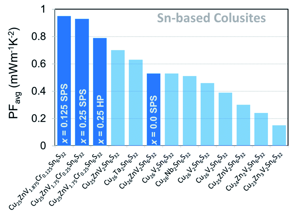 | ||
| Fig. 8 Average PF values of Sn-based colusites in their respective measured temperature ranges. Darker blue color indicates compounds in this work.47,50,52,56 | ||
The temperature dependence of the total (κ) and lattice (κlat) part of the thermal conductivity is shown in Fig. 6d and e. For x = 0, a κ value of 0.83 W m−1 K−1 is obtained at 300 K, which decreases monotonically to 0.73 W m−1 K−1 at 700 K. The κlat of all the samples shows a 1/T dependence (Fig. 6e), which indicates the dominant Umklapp phonon scattering process. This result is in line with the values observed by Kim et al. for the same composition.56 On the other hand, κ increases with varying the Cr content and reaches the highest value of 2.66 W m−1 K−1 and 1.79 W m−1 K−1, respectively, at 300 K and 700 K for x = 0.375. From x = 0 up to x = 0.25; κ increases significantly over the entire temperature range due, almost equally, to the increase of electronic (κel) and phonon contributions (κlat – Fig. 6e). This second contribution enhancement agrees with the reduced perturbation of the structural network by the Cr cation owing to its smaller cationic size. Therefore, it is reasonable to expect that both thermal and electrical transport are favoured due to the reduced distortion of the Cu–S network. For x > 0.25, κ reaches saturation values. The increase of the κel with Cr content is counterbalanced by the presence of the secondary phase that affects the scattering mechanism and contributes to lowering the κlat.
Finally, the temperature dependence of the dimensionless figure of merit, zT, is given in Fig. 6f. All samples exhibit a linear temperature dependence of zT with a maximum value of 0.60 at 700 K for x = 0 and x = 0.125. Despite the beneficial effect of Cr-substitution in the Sn-based colusite PF, the overall zT remained comparable to that of the undoped sample due to the offset made by the κ increase. However, it motivates the following study to combine the positive effect of Cr-substitution with the cationic disorder induced by hot press sintering to achieve a lower κ.
3.6 Optimization of the zT: hot-pressing method
A further enhancement of zT is possible by optimizing electrical and thermal properties, especially loweringκ without influencing the PF significantly. For example, Bourgès et al. reported that appropriate densification strategies might induce the scattering of short-wavelength phonons attributed to sulfur vacancies and cationic disorder, resulting in lower thermal conductivity.48 A significant reduction of κlat was achieved for sample Cu26V2Sn6S32 in the whole temperature range from 1.3 W m−1 K−1 at 300 K, sintered at 873 K with the SPS method, to 0.3 W m−1 K−1 at 300 K, sintered at 1023 K with the hot-pressing (HP) method. Moreover, the HP promotes a Cu/S off-stoichiometry favorable to a larger lattice due to the incorporation of Cu into the interstitial site by the higher sintering temperature as described in the previous section (cf. 3.4).59 Thus the larger lattice size induction will help to maintain a superior S and reduce the significant drop of the S induced by Cr co-doping.In this section, the optimization of TE properties was carried out for the samples Cu25ZnV2−xCrxSn6S32 (x = 0, 0.25 and 0.5) by hot-press sintering. The PXRD of the HPed samples showed the single-phase formation for x ≤ 0.25 (Fig. S8†), confirming again the apparent Cr solubility limit with the presence of a tiny amount of CuS in sample x = 0.5, which is further evidenced by EDS (Fig. S9–S11†). These results are in line with the SPSed samples. The Le Bail refinement of the lattice parameter revealed that the HP approach enables the possibility of maintaining a large lattice (a > 10.81 Å) in the Sn-based colusite as expected (Table 3). Indeed, the HP process at a high temperature (T = 923 K) favored a higher loss of sulfur, leading to a cationic rich stoichiometry. It has been reported that this extra cation could occupy a relatively sizeable interstitial void 6b (0, 0, ½) present within the colusite structure, forming an additional tetrahedron in the colusite structure, which, consequently, would enlarge the lattice.59 In the present case, all the HPed samples showed a Cu-rich composition (Fig. S9–S11†) sustaining a plausible filling of the interstitial 6b site with an extra Cu atom. It can be noticed that the x = 0.25 sample has an even larger lattice parameter than the x = 0 sample, which is most likely due to the process uncertainty. All samples were systematically prepared by using a rigorous procedure. However, it cannot be excluded that excess sulfur volatilization could occur and induce a larger amount of interstitial cations leading to this larger lattice parameter, despite Cr doping for the x = 0.25 sample.
| Cu26ZnV2−xCrxSn6S32 | ||
|---|---|---|
| x | SPS-a (Å) | HP-a (Å) |
| 0 | 10.834 | 10.815 |
| 0.125 | 10.802 | — |
| 0.25 | 10.776 | 10.821 |
| 0.375 | 10.774 | — |
| 0.5 | 10.779 | 10.811 |
The enlarged lattice induced by the HP does not significantly affect the Sn-based colusite microstructure (Fig. S12†) compared to the SPSed samples. All samples showed a similar microstructure regardless of the Cr content. Compared to the SPSed samples, the grain size of all the samples is distributed with uniform size and shape. In addition, homogeneous distribution of inter-granular nanoporosity in the matrix is still observed.
The TE properties in the range of 300 to 700 K of HPed compounds are shown in Fig. 9. In line with the previous SPSed sample results, the ρ is suppressed by 40–60% in the whole temperature range for the samples with Cr-doping by comparison with the pristine sample. However, the significant drop of the S, observed initially in the Cr-doped SPSed samples, is dampened, likely by the proficient effect of lattice enlargement. We can observe that the S of the HPed sample x = 0.25 is reduced by only ∼10–20% compared to ∼30–50% in the corresponding SPSed series. Thanks to this, the global PF remains improved mainly by the Cr-doping effect (Fig. 8 and 9c), especially for the x = 0.25 sample with a remarkable PFave ≈ 0.8 mW m−1 K−2 in the temperature range of 300–700 K.
 | ||
| Fig. 9 Temperature dependence of (a) electrical resistivity ρ, (b) Seebeck coefficient S, (c) thermal conductivity κ, (d) lattice thermal conductivity κlat, (e) power factor PF, and (f) dimensionless thermoelectric figure of merit zT for hot-pressed Cu–Sn compounds. | ||
Fig. 9d shows that the thermal conductivity of the HPed samples is significantly reduced as compared to the SPSed samples. The reduction of κ is mainly attributed to the flattening of κlat induced by the enhanced phonon scattering. This remarkable reduction in κ is consistent with the intrinsic defect chemistry of the Sn-based colusite.48,49 The Sn-based colusites have a strong tendency to form SnCu antisite defects, which is supported by the total energy calculations.48 Within the structure, this leads to the natural formation of a 1D-line defect. Higher sintering temperature or additional heat treatment exacerbated the phenomenon to form an apparent completely disordered crystalline area.
As a consequence of the cationic disorder induced, the κlat is strongly decreased in our HPed samples. It can be pointed out that the heat treatment at a higher temperature (T = 923 K) can also promote a sulfur deficiency/vacancy susceptible to enhancing the scattering of the short-wavelength phonons. To clarify, a nearly glass-like behavior has already been reported with a κlat of 0.27 W m−1 K−1 corresponding to the minimal theoretical value predicted by the Cahill and Pohl model.48,87 In this study, a minimum κlat of 0.5 W m−1 K−1 at 700 K has been obtained for the sample x = 0.25, proving that the defect density of our samples implied by the process control is likely lower than the previous results, which agrees with the slightly lower sintering temperature employed.
Thus leads to an increase of the zT, resulting in the maximum value of 0.8 at 700 K for x = 0.25. This validates the concept of combining process engineering to tune the thermal transport properties and the proficient Cr-doping effect to enhance the TE properties.
4. Conclusion
We have reported the first successful Cr incorporation within the bulk Sn-based colusite structure and revealed a major insight regarding the lattice size effect on this attractive TE compound. To reach this goal, we employed a multi-directional approach: (1) by process engineering using a mixed synthesis, combining a sealed tube reaction method and ball milling before a final densification step to avoid the formation of secondary phases and strengthen the mechanical properties; (2) by lattice engineering using co-doping of the Cu site with Zn to enlarge the crystal lattice and stabilize the natural exsolution phenomenon present within the Sn-based colusite. We demonstrated that both approaches are required to open a narrow window of solubility of Cr within the Sn-based structure (x < 0.375 for Cu26ZnV2−xCrxSn6S32). As a result, we achieved the highest PF of 1.1–1.2 mW m−1 K−2 at 700 K so far reported in Sn-based colusites. Employing the proficient effect of the Cr-doping, we were able to substantially enhance the electrical conductivity. This fortuituous effect has been linked to various features including carrier tuning, effective mass reduction, and a novel highlight related to lattice contribution in the Seebeck coefficient. Our finding revealed that modulation of the lattice size of the Sn-based colusite could affect its Seebeck coefficient by 30 to 50 μV K−1 depending on the carrier concentration. Theoretical evidence supports all the experimental results, including spin-polarized DOS and band structure calculation. Using this unique finding, we finally optimized the compound by HP treatment to selectively lower the κ, and reported a competitive zT value of 0.8 at 700 K for the sample Cu25ZnV1.75Cr0.25Sn6S32. This result opens a new route for this scalable TE compound to achieve higher performance by including the lattice engineering contribution in the already existing process/defect chemistry/doping strategies. This approach can also be considered in other complex TE sulfide materials where the defect chemistry plays an essential role in the lattice size and, therefore, performance.Author contributions
Conceptualization, C. B. and T. M.; methodology, P. K., C. B., D. G. and T. N.; software, P. K., P. S., and W. S.; validation, C. B., R. C, W. S and T. M.; formal analysis, P. K., and C. B.; investigation, P. K. and C. B.; resources, W. S, T. N. and T. M.; visualization, P. K. and C. B.; data curation, P. K., C. B., and R. C.; writing—original draft preparation, P. K. and C. B.; writing—review and editing, P. K., C. B., R. C., D. G., P. S, W. S., and T. M.; supervision, C. B., W. S., and T. M.; funding acquisition, W. S., and T. M. All authors have read and agreed to the published version of the manuscript.Conflicts of interest
The authors declare no conflict of interest.Acknowledgements
P. K. would like to acknowledge the financial support of the International Cooperative Graduate Program funded by the National Institute for Materials Science in Japan. This research was also financially supported by the Polish National Science Centre under Contract No. UMO2018/29/N/ST8/01565. Computing resources were provided by the Poznan Supercomputing and Networking Center (PSNC) under Grant No. 427. C. B., R. C., D. G. and T. M acknowledge support from JST Mirai Program grant nos. JPMJMI19A1 and JSPS KAKENHI JP19H00833. The authors would like to thank Namiki foundry (NIMS, Japan) for the use of the SEM facilities.References
- Y. Xiao and L. D. Zhao, Science, 2020, 367, 1196–1197 CrossRef CAS PubMed.
- I. Petsagkourakis, K. Tybrandt, X. Crispin, I. Ohkubo, N. Satoh and T. Mori, Sci. Technol. Adv. Mater., 2018, 19, 836–862 CrossRef CAS PubMed.
- T. Xing, Q. Song, P. Qiu, Q. Zhang, M. Gu, X. Xia, J. Liao, X. Shi and L. Chen, Energy Environ. Sci., 2021, 14, 995–1003 RSC.
- Z. Liu, N. Sato, W. Gao, K. Yubuta, N. Kawamoto, M. Mitome, K. Kurashima, Y. Owada, K. Nagase, C. H. Lee, J. Yi, K. Tsuchiya and T. Mori, Joule, 2021, 5, 1196–1208 CrossRef CAS.
- B. Zhu, X. Liu, Q. Wang, Y. Qiu, Z. Shu, Z. Guo, Y. Tong, J. Cui, M. Gu and J. He, Energy Environ. Sci., 2020, 13, 2106–2114 RSC.
- Q. Zhang, Y. Lin, N. Lin, Y. Yu, F. Liu, C. Fu, B. Ge, O. Cojocaru-Mirédin, T. Zhu and X. Zhao, Mater. Today Phys., 2022, 22, 100573 CrossRef CAS.
- H. Jang, J. H. Park, H. S. Lee, B. Ryu, S. D. Park, H. A. Ju, S. H. Yang, Y. M. Kim, W. H. Nam, H. Wang, J. Male, G. J. Snyder, M. Kim, Y. S. Jung and M. W. Oh, Adv. Sci., 2021, 8, 1–11 Search PubMed.
- Z.-Z. Luo, S. Cai, S. Hao, T. P. Bailey, Y. Luo, W. Luo, Y. Yu, C. Uher, C. Wolverton, V. P. Dravid, Z. Zou, Q. Yan and M. G. Kanatzidis, Energy Environ. Sci., 2022, 15, 368–375 RSC.
- J. Shuai, Y. Sun, X. Tan and T. Mori, Small, 2020, 16, 1–7 CrossRef PubMed.
- Z. Liu, W. Gao, W. Zhang, N. Sato, Q. Guo and T. Mori, Adv. Energy Mater., 2020, 10, 1–8 Search PubMed.
- X. Wang, X. Li, Z. Zhang, X. Li, C. Chen, S. Li, X. Lin, J. Sui, X. Liu, F. Cao, J. Yang and Q. Zhang, Mater. Today Phys., 2018, 6, 45–52 CrossRef.
- O. Caballero-Calero, J. R. Ares and M. Martín-González, Adv. Sustainable Syst., 2021, 5, 2100095 CrossRef CAS.
- A. V. Powell, J. Appl. Phys., 2019, 126, 100901 CrossRef.
- Y. He, T. Day, T. Zhang, H. Liu, X. Shi, L. Chen and G. J. Snyder, Adv. Mater., 2014, 26, 3974–3978 CrossRef CAS PubMed.
- Y. Yao, B. P. Zhang, J. Pei, Y. C. Liu and J. F. Li, J. Mater. Chem. C, 2017, 5, 7845–7852 RSC.
- K. Zhao, A. B. Blichfeld, H. Chen, Q. Song, T. Zhang, C. Zhu, D. Ren, R. Hanus, P. Qiu, B. B. Iversen, F. Xu, G. J. Snyder, X. Shi and L. Chen, Chem. Mater., 2017, 29, 6367–6377 CrossRef CAS.
- P. Nieroda, J. Leszczyński, A. Mikuła, K. Mars, M. J. Kruszewski and A. Koleżyński, Ceram. Int., 2020, 46, 25460–25466 CrossRef CAS.
- P. Qiu, T. Zhang, Y. Qiu, X. Shi and L. Chen, Energy Environ. Sci., 2014, 7, 4000–4006 RSC.
- S. O. J. Long, A. V. Powell, P. Vaqueiro and S. Hull, Chem. Mater., 2018, 30, 456–464 CrossRef CAS.
- A. Zhang, B. Zhang, W. Lu, D. Xie, H. Ou, X. Han, J. Dai, X. Lu, G. Han, G. Wang and X. Zhou, Adv. Funct. Mater., 2018, 28, 1–8 Search PubMed.
- L. Guo, B. Zhang, H. Zhu, H. Wu, Y. Yan, X. Gong, X. Lu, G. Han, G. Wang and X. Zhou, J. Mater. Chem. C, 2020, 8, 17222–17228 RSC.
- H. Takaki, K. Kobayashi, M. Shimono, N. Kobayashi, K. Hirose, N. Tsujii and T. Mori, Mater. Today Phys., 2017, 3, 85–92 CrossRef.
- J. Li, Q. Tan and J. F. Li, J. Alloys Compd., 2013, 551, 143–149 CrossRef CAS.
- N. Tsujii, T. Mori and Y. Isoda, J. Electron. Mater., 2014, 43, 2371–2375 CrossRef CAS.
- N. Sato, P. S. Gan, N. Tsujii and T. Mori, Appl. Phys. Express, 2021, 14, 1–5 Search PubMed.
- D. Zhang, B. Zhang, Z. Zhou, K. Peng, H. Wu, H. Wang, G. Wang, G. Han, G. Wang, X. Zhou and X. Lu, Chem. Mater., 2021, 33, 9795–9802 CrossRef CAS.
- H. Xie, X. Su, T. P. Bailey, C. Zhang, W. Liu, C. Uher, X. Tang and M. G. Kanatzidis, Chem. Mater., 2020, 32, 2639–2646 CrossRef CAS.
- R. Ang, A. U. Khan, N. Tsujii, K. Takai, R. Nakamura and T. Mori, Angew. Chem., Int. Ed., 2015, 54, 12909–12913 CrossRef CAS PubMed.
- K. Hashikuni, K. Suekuni, H. Usui, R. Chetty, M. Ohta, K. Kuroki, T. Takabatake, K. Watanabe and M. Ohtaki, Inorg. Chem., 2019, 58, 1425–1432 CrossRef CAS PubMed.
- C. Bourgès, B. Srinivasan, B. Fontaine, P. Sauerschnig, A. Minard, J. F. Halet, Y. Miyazaki, D. Berthebaud and T. Mori, J. Mater. Chem. C, 2020, 8, 16368–16383 RSC.
- A. U. Khan, R. A. R. Al Orabi, A. Pakdel, J. B. Vaney, B. Fontaine, R. Gautier, J. F. Halet, S. Mitani and T. Mori, Chem. Mater., 2017, 29, 2988–2996 CrossRef CAS.
- C. Bourgès, V. Pavan Kumar, H. Nagai, Y. Miyazaki, B. Raveau and E. Guilmeau, J. Alloys Compd., 2019, 781, 1169–1174 CrossRef.
- C. Bourgès, P. Lemoine, O. I. Lebedev, R. Daou, V. Hardy, B. Malaman and E. Guilmeau, Acta Mater., 2015, 97, 180–190 CrossRef.
- T. He, N. Lin, Z. Du, Y. Chao and J. Cui, J. Mater. Chem. C, 2017, 5, 4206–4213 RSC.
- D. Zhang, J. Yang, Q. Jiang, Z. Zhou, X. Li, J. Xin, A. Basit, Y. Ren and X. He, Nano Energy, 2017, 36, 156–165 CrossRef CAS.
- E. Isotta, B. Mukherjee, C. Fanciulli, N. M. Pugno and P. Scardi, J. Phys. Chem. C, 2020, 124, 7091–7096 CrossRef CAS.
- C. Bourgès, R. Al Rahal Al Orabi and Y. Miyazaki, J. Alloys Compd., 2020, 826, 1–9 CrossRef.
- Q. Jiang, H. Yan, Y. Lin, Y. Shen, J. Yang and M. J. Reece, J. Mater. Chem. A, 2020, 8, 10909–10916 RSC.
- A. Nagaoka, K. Yoshino, T. Masuda, T. D. Sparks, M. A. Scarpulla and K. Nishioka, J. Mater. Chem. A, 2021, 9, 15595–15604 RSC.
- X. Lu, D. T. Morelli, Y. Xia and V. Ozolins, Chem. Mater., 2015, 27, 408–413 CrossRef CAS.
- K. Suekuni, K. Tsuruta, T. Ariga and M. Koyano, Appl. Phys. Express, 2012, 5, 051201 CrossRef.
- J. Heo, G. Laurita, S. Muir, M. A. Subramanian and D. A. Keszler, Chem. Mater., 2014, 26, 2047–2051 CrossRef CAS.
- S. Tippireddy, R. Chetty, M. H. Naik, M. Jain, K. Chattopadhyay and R. C. Mallik, J. Phys. Chem. C, 2018, 122, 8735–8749 CrossRef CAS.
- R. Chetty, A. Bali, M. H. Naik, G. Rogl, P. Rogl, M. Jain, S. Suwas and R. C. Mallik, Acta Mater., 2015, 100, 266–274 CrossRef CAS.
- H. Hu, H. L. Zhuang, Y. Jiang, J. Shi, J. W. Li, B. Cai, Z. Han, J. Pei, B. Su, Z. H. Ge, B. P. Zhang and J. F. Li, Adv. Mater., 2021, 33, 1–10 Search PubMed.
- X. Lu, D. T. Morelli, Y. Xia, F. Zhou, V. Ozolins, H. Chi, X. Zhou and C. Uher, Adv. Energy Mater., 2013, 3, 342–348 CrossRef CAS.
- K. Suekuni, F. S. Kim, H. Nishiate, M. Ohta, H. I. Tanaka and T. Takabatake, Appl. Phys. Lett., 2014, 105, 132107 CrossRef.
- C. Bourgès, Y. Bouyrie, A. Supka, R. Al Rahal Al Orabi, P. Lemoine, O. Lebedev, M. Ohta, K. Suekuni, V. Nassif, V. Hardy, R. Daou, Y. Miyazaki, M. Fornari and E. Guilmeau, J. Am. Chem. Soc., 2018, 140, 2186–2195 CrossRef PubMed.
- G. Guélou, P. Lemoine, B. Raveau and E. Guilmeau, J. Mater. Chem. C, 2021, 9, 773–795 RSC.
- C. Bourgès, M. Gilmas, P. Lemoine, N. Mordvinova, O. I. Lebedev, E. Hug, V. M. Nassif, B. Malaman, R. Daou and E. Guilmeau, J. Mater. Chem. C, 2016, 4, 7455–7463 RSC.
- G. Guélou, C. Couder, C. Manière, C. Candolfi, B. Lenoir, L. Lallemant, C. Coureau and E. Guilmeau, Appl. Mater. Today, 2021, 22, 100948 CrossRef.
- Y. Kikuchi, Y. Bouyrie, M. Ohta, K. Suekuni, M. Aihara and T. Takabatake, J. Mater. Chem. A, 2016, 4, 15207–15214 RSC.
- V. Pavan Kumar, A. R. Supka, P. Lemoine, O. I. Lebedev, B. Raveau, K. Suekuni, V. Nassif, R. Al Rahal Al Orabi, M. Fornari and E. Guilmeau, Adv. Energy Mater., 2019, 9, 1–11 Search PubMed.
- T. Hagiwara, K. Suekuni, P. Lemoine, A. R. Supka, R. Chetty, E. Guilmeau, B. Raveau, M. Fornari, M. Ohta, R. Al Rahal Al Orabi, H. Saito, K. Hashikuni and M. Ohtaki, Chem. Mater., 2021, 33, 3449–3456 CrossRef CAS.
- K. Suekuni, F. Kim and T. Takabatake, J. Appl. Phys., 2014, 116, 063706 CrossRef.
- F. S. Kim, K. Suekuni, H. Nishiate, M. Ohta, H. I. Tanaka and T. Takabatake, J. Appl. Phys., 2016, 119, 175105 CrossRef.
- V. Pavan Kumar, S. Mitra, G. Guélou, A. R. Supka, P. Lemoine, B. Raveau, R. Al Rahal Al Orabi, M. Fornari, K. Suekuni and E. Guilmeau, Appl. Phys. Lett., 2020, 117, 6–11 CrossRef.
- V. Pavan Kumar, G. Guélou, P. Lemoine, B. Raveau, A. R. Supka, R. Al Rahal Al Orabi, M. Fornari, K. Suekuni and E. Guilmeau, Angew. Chem., Int. Ed., 2019, 58, 15455–15463 CrossRef CAS PubMed.
- K. Suekuni, Y. Shimizu, E. Nishibori, H. Kasai, H. Saito, D. Yoshimoto, K. Hashikuni, Y. Bouyrie, R. Chetty, M. Ohta, E. Guilmeau, T. Takabatake, K. Watanabe and M. Ohtaki, J. Mater. Chem. A, 2019, 7, 228–235 RSC.
- G. Guélou, C. Couder, A. Bourhim, O. I. Lebedev, N. Daneu, F. Appert, J. Juraszek, P. Lemoine, L. Segreto and E. Guilmeau, Acta Mater., 2020, 195, 229–239 CrossRef.
- M. Hegedüs, M. Achimovičová, H. Hui, G. Guélou, P. Lemoine, I. Fourati, J. Juraszek, B. Malaman, P. Baláž and E. Guilmeau, Dalton Trans., 2020, 49, 15828–15836 RSC.
- P. Lemoine, V. Pavan Kumar, G. Guélou, V. Nassif, B. Raveau and E. Guilmeau, Chem. Mater., 2020, 32, 830–840 CrossRef CAS.
- R. Chetty, P. Jood, M. Murata, K. Suekuni and M. Ohta, Appl. Phys. Lett., 2022, 120, 013501 CrossRef CAS.
- Y. You, X. Su, S. Hao, W. Liu, Y. Yan, T. Zhang, M. Zhang, C. Wolverton, M. G. Kanatzidis and X. Tang, J. Mater. Chem. A, 2018, 6, 15123–15131 RSC.
- K. Zhang, H. Wang, W. Su, T. Wang, X. Wang, T. Chen, T. Huo, F. Dang, M. Dong, C. Wang, B. Dong and Z. Guo, J. Phys. D: Appl. Phys., 2020, 53, 245501 CrossRef CAS.
- S. Hu, J. Xiao, J. Zhou, S. R. Elliott and Z. Sun, J. Mater. Chem. C, 2020, 8, 6672–6679 RSC.
- X. Tan, G. Liu, J. Xu, X. Tan, H. Shao, H. Hu, H. Jiang, Y. Lu and J. Jiang, J. Mater., 2018, 4, 62–67 Search PubMed.
- J. Rodríguez-Carvajal, Phys. B, 1993, 192, 55–69 CrossRef.
- T. Roisnel and J. Rodríguez-Carvajal, in Materials Science Forum, Trans Tech Publications Ltd, 2001, vol. 378–381, pp. 118–123 Search PubMed.
- A. Le Bail, Powder Diffr., 2005, 20, 316–326 CrossRef CAS.
- H. S. Kim, Z. M. Gibbs, Y. Tang, H. Wang and G. J. Snyder, APL Mater., 2015, 3, 1–6 Search PubMed.
- D. Joubert, Phys. B, 1999, 59, 1758–1775 Search PubMed.
- P. E. Blöchl, Phys. Rev. B, 1994, 50, 17953–17979 CrossRef PubMed.
- G. Kresse and J. Furthmüller, Phys. B, 1996, 54, 11169–11186 CAS.
- G. Pizzi, D. Volja, B. Kozinsky, M. Fornari and N. Marzari, Comput. Phys. Commun., 2014, 185, 422–429 CrossRef CAS.
- G. Chen, Nanoscale Energy Transport and Conversion, Oxford University Press, 2005 Search PubMed.
- A. F. May, E. S. Toberer, A. Saramat and G. J. Snyder, Phys. B, 2009, 80, 1–12 Search PubMed.
- R. D. Shannon, Acta Crystallogr., Sect. A: Cryst. Phys., Diffr., Theor. Gen. Crystallogr., 1976, 32, 751–767 CrossRef.
- K. Suekuni, H. I. Tanaka, F. S. Kim, K. Umeo and T. Takabatake, J. Phys. Soc. Jpn., 2015, 84, 2–5 CrossRef.
- Z. C. Cordero, B. E. Knight and C. A. Schuh, Int. Mater. Rev., 2016, 61, 495–512 CrossRef CAS.
- C. Candolfi, G. Guélou, C. Bourgès, A. R. Supka, R. Al Rahal Al Orabi, M. Fornari, B. Malaman, G. Le Caër, P. Lemoine, V. Hardy, J. M. Zanotti, R. Chetty, M. Ohta, K. Suekuni and E. Guilmeau, Phys. Rev. Mater., 2020, 4, 25404 CrossRef CAS.
- T. Mori, Small, 2017, 13, 1702013 CrossRef PubMed.
- Y. Zheng, T. Lu, M. H. Polash, M. Rasoulianboroujeni, N. Liu, M. E. Manley and Y. Deng, Sci. Adv., 2019, 5, 1–8 Search PubMed.
- J. B. Vaney, S. Aminorroaya Yamini, H. Takaki, K. Kobayashi, N. Kobayashi and T. Mori, Mater. Today Phys., 2019, 9, 100090 CrossRef.
- D. Berthebaud, O. I. Lebedev and A. Maignan, J. Appl. Phys., 2018, 124, 063905 CrossRef.
- S. Hébert, R. Daou, A. Maignan, S. Das, A. Banerjee, Y. Klein, C. Bourgès, N. Tsujii and T. Mori, Sci. Technol. Adv. Mater., 2021, 22, 583–596 CrossRef PubMed.
- D. Cahill, S. K. Watson and R. O. Pohl, Am. Phys. Soc., 1992, 46, 6131–6140 CAS.
Footnote |
| † Electronic supplementary information (ESI) available. See https://doi.org/10.1039/d2ta01210c. |
| This journal is © The Royal Society of Chemistry 2022 |