
 Open Access Article
 This Open Access Article is licensed under a
 Creative Commons Attribution 3.0 Unported Licence
High thermoelectric performance based on CsSnI3 thin films with improved stability†
Weidong
Tang
 ,
Tianjun
Liu
and
Oliver
Fenwick
*
,
Tianjun
Liu
and
Oliver
Fenwick
*
School of Engineering and Materials Science, Queen Mary University of London, Mile End Road, London E1 4NS, UK. E-mail: o.fenwick@qmul.ac.uk
First published on 16th March 2022
Abstract
Tin-based metal halide perovskites have been considered as promising candidates in the field of thermoelectric materials due to their ultralow thermal conductivity and considerable electrical conductivity. However, the mechanism of air exposure to self-dope the films for enhanced thermoelectric properties raises questions about their stability for thermoelectric applications. Here, we report increased air stability of sequential thermally evaporated CsSnI3 thin films without using any additives. This was achieved by adjustment of the order of deposition of the precursor materials. The optimised films show more than an order of magnitude less degradation in electrical conductivity in air over 60 minutes than control samples and have optical signatures of degradation in air that take ∼5 times longer to emerge. Conversely, we show that the rate of self-doping through oxidation of Sn2+ to Sn4+ is substantially enhanced at elevated temperatures and characterise its impact on thermal and electrical transport properties. Furthermore, we obtain a figure of merit (zT) of 0.08 for CsSnI3 thin films in this more stable configuration.
Introduction
To meet the energy demands of our society, carbon emissions are increasing and global warming is a reality. As a result, many countries have decided to aim for a carbon-neutral status by the middle of the 21st century.1 Using low-carbon energy (wind energy, solar energy, nuclear energy, and tidal energy) to generate electricity has become increasingly popular, but the dominant source of electricity still comes from fossil fuels (coal, gas, and oil). The efficiency of these power plants is typically up to 45%,2 with the remaining 55% emitted as low-grade waste heat. Moreover, a lot of waste heat is emitted at the point of customer use, including from car engines and electronic devices, as well as from living organisms. How to use this waste heat and convert it back into useful energy for human use is an active area of research.Thermoelectric generators (TEGs) are semiconductor devices that can directly convert waste heat into electricity from temperature gradients, exploiting a thermal voltage generated through the Seebeck effect.3 The performance of thermoelectric materials is often judged by the thermoelectric figure of merit, zT:
| zT = S2σT/κ |
Metal halide perovskites have been considered as next generation photovoltaic materials, achieving a power efficiency over 20% (ref. 5–8) for solar cells with single-junction architectures. Because of their high absorption coefficients, high charge carrier mobilities, solution processability, large carrier diffusion lengths, high photoluminescence quantum yields (PLQYs) and tuneable bandgap, halide perovskites have also been developed for LEDs, photodetectors and lasers.9–15 In 2014, ab initio calculations were used to show that metal halide perovskites may be useful thermoelectric materials.16 It was also found that, due to the large carrier mobilities originating from the small effective masses of charges and a poor carrier–phonon interaction, the zT of CH3NH3AI3 (A = Pb and Sn) might be optimised to between 1 and 2 by tuning the charge carrier density to the order of 1018 cm−3. Recent studies have predicted zT as high as 2.6 in low dimensional metal halide perovskite derivatives.17 Many experimental studies have reported metal halide perovskites with high Seebeck coefficient,18,19 and ultra-low thermal conductivity,20–25 and have also reported doping methods to tune their electrical conductivity.20,22,26 However, doping of halide perovskite materials remains challenging, which may be due to ionic compensation of charged point defects27 and a defect tolerant electronic structure deriving from bonding orbitals at the conduction band minimum (CBM) as well as antibonding orbitals at the valence band maximum (VBM).28 Substitutional doping of a Pb-perovskite with Bi3+, has been shown to increase conductivity by 4 orders of magnitude, but the conductivity and zT remained low.20 However, tin-based halide perovskites show metallic conductivity caused by self-doping related to Sn2+ to Sn4+ oxidation.29,30 Our previous work achieved a zT of 0.14 for CsSnI3−xClx thin films with enhanced stability over non-chlorine containing films.26
In this work, we thermally evaporated CsSnI3 thin films by two different recipes. Both methods involve sequential deposition of the precursors (CsI and SnI2), but differ in the order of deposition. Importantly, we do not use additives such as substitutions on the A, B or X-site in the ABX3 structure that are typically used to improve stability. All of our films show a pinhole-free morphology with micrometre-sized grains. We find that SCS films (SnI2 deposited before CsI) retain 73% of their absorption at 420 nm after 10 hours air exposure, whereas for CSS films (CsI deposited before SnI2) only 24% of the absorption is retained after 10 hours.26,31 Furthermore, the SCS films show 13 times less degradation in electrical conductivity in air over 60 minutes than the CSS films. Additionally, we measured the thermoelectric properties of our films oxidised at room temperature and 80 °C. We found our films oxidised at room temperature are quite stable and their thermoelectric properties show only modest changes with increasing oxidation time. However, films oxidised at 80 °C displayed a rapid growth of electrical conductivity and thermal conductivity, and a moderate decrease of Seebeck coefficient over periods of 15 minutes. X-ray photoelectron spectroscopy was used to confirm elemental composition and Sn oxidation states. It revealed that the Sn2+ to Sn4+ self-doping process happens from surface to bulk, and this process is accelerated by oxidation temperature. We achieved a zT of 0.08 for SCS films at both 333 K and 343 K after 3 minutes air exposure at 80 °C.
Experimental methods
Materials
Stannous(II) iodide (SnI2, anhydrous, 99.99% trace metals basis) and caesium iodide (CsI, anhydrous, 99.9% trace metals basis) were purchased from Sigma Aldrich. All salts were opened in a nitrogen glovebox (H2O < 0.1 ppm and O2 < 0.1 ppm) without any air exposure and used as received without any further purification.Deposition of CsSnI3 thin films
A sequential thermal evaporation method was used to deposit CsSnI3 thin films. For the CsI/SnI2 sequential deposition method (CSS), CsI was first thermally evaporated at 170 °C, followed by SnI2 at 420 °C. For SnI2/CsI sequential deposition method (SCS), SnI2 was first thermally evaporated at 420 °C, followed by CsI at 170 °C. For both methods, the deposition rates of CsI and SnI2 were approximately 6 Å s−1 and 2 Å s−1, respectively. The deposited thicknesses of CsI and SnI2 were 100 ± 10 nm each. The whole deposition process proceeded at 10−7 mbar in the dark, without any break in the vacuum. After thermal evaporation, the sepia coloured thin films were removed from the vacuum chamber and annealed at 170 °C on a hotplate in a nitrogen filled glove box. After annealing, the films became mirror-black (Fig. S1†), which gives an initial indication of the successful synthesis of CsSnI3 thin films in the orthorhombic B-γ phase.X-ray photoelectron spectroscopy (XPS)
XPS measurements were performed on thermally evaporated thin films (200–250 nm thick) with a Thermo Scientific™ Nexsa™ Surface Analysis System, using a 200 × 200 μm size X-ray spot from an Al Kα source. Samples were exposed to air for 5 minutes either at room temperature or at 80 °C and then loaded into the XPS vacuum chamber which was under high vacuum (<10−8 mbar). Depth profiles were achieved by etching with Ar+ ions for 3 seconds per level using a 2 keV accelerating voltage. The depth profile was calibrated from the etching time corresponding to the etching thickness (from the film surface to the silicon substrate). All XPS spectra were recorded and processed using the Thermo Avantage software.X-ray diffraction (XRD)
XRD measurements were performed on a D5000 X-ray Diffractometer (Siemens) over a 2θ range between 5° and 70° using a Cu Kα source.Scanning electron microscopy (SEM)
The morphological properties of the films were observed on a field-emission scanning electron microscope (FEI Inspect-F). The parameters for the collection of SEM pictures were accelerating voltage 20.00 kV, magnification 25![[thin space (1/6-em)]](https://www.rsc.org/images/entities/char_2009.gif) 000× and working distance 9.7 mm for SCS films and accelerating voltage 20.00 kV, magnification 16000× and working distance 10.8 mm for CSS films.
000× and working distance 9.7 mm for SCS films and accelerating voltage 20.00 kV, magnification 16000× and working distance 10.8 mm for CSS films.
Optical absorption
UV-Vis absorption spectra were measured for CsSnI3 thin films (200–250 nm thick) on glass substrates with a Shimadzu UV-2600 spectrophotometer. The time-dependent air stability measurement used 10 minute intervals (60 cycles) over a 10 hour period.Nitrogen and ambient electrical conductivity measurement
The in-plane electrical conductivity measurements were performed on a four-point probe station (Ossila) with a Keithley 2400 Series SMU (note: for these measurements the perovskite films were directly deposited on glass substrates). In both cases the first measurement was taken in the nitrogen filled glove box with subsequent measurements either taken in the glovebox (O2 and H2O < 1 ppm) or in air.Thermoelectric property measurement
The in-plane thermoelectric property measurements were performed on a Linseis Thin Film Analyser (TFA). The pre-patterned measurement chips with CsSnI3 thin films deposited on top (200 nm thick) are shown in Fig. S8.† A description of the measurement (electrical conductivity by the van der Pauw method, Seebeck coefficient and thermal conductivity by the 3-ω method) is provided elsewhere26,32,33 For the oxidation time-dependent measurements, the sample was initially measured after transferring to the TFA and evacuating to 10−5 mbar. After the first measurement, it was oxidised in situ in the TFA chamber for 3 minutes by refilling the chamber with air and then was measured again after evacuating back to 10−5 mbar.Results
We present two sequential methods to deposition CsSnI3 thin films, which differ by the order of the precursors deposited. For the CSS method (Fig. 1a), a CsI layer is thermally evaporated first, followed by a SnI2 layer. For the SCS method (Fig. 1b), the first thermal evaporation is SnI2, followed by CsI. SCS and CSS bilayer films were both baked at 170 °C to form CsSnI3 perovskite thin films (Fig. 1c). For both CSS and SCS thin films, the initial colour was sepia and then became mirror-black after annealing at 170 °C (Fig. S1†), which is an initial indication of formation of the orthorhombic B-γ phase. SEM analysis (Fig. 1d and e) shows that both CSS and SCS CsSnI3 thin films are pinhole free and have tightly packed grains, typical of halide perovskite films. The CSS films have an average grain size of 0.71 μm2, whereas the SCS thin films have a slightly larger average grain size of 1.1 μm2 (Fig. S2†). Our films have the typical halide perovskite morphology and our grain sizes are quite large, compared to many other Sn-based perovskite deposition methods.31,34–36 XRD spectra (Fig. 1f) show that both films are in the black-γ phase, corresponding to the orthorhombic structure of CsSnI3. Both CsSnI3 films show peaks at 14.50°, 20.65°, 23.05°, 24.15°, 25.25° and 29.15° (2θ) corresponding to the (020), (200), (201), (031), (220) and (202) planes, respectively, which indicates that crystallites in the films have mixed orientation,30 but both films have the same dominant (202) peak indicating a shared preferential orientation. Nonetheless, there are small differences such as the CSS film displaying the (040) peak at 27.67° (2θ) which is not evident XRD spectra of SCS film. Tauc plots of the absorbance of our CSS and SCS films indicate a bandgap of 1.36 eV in both cases (Fig. S14†), which is in agreement with computed values.30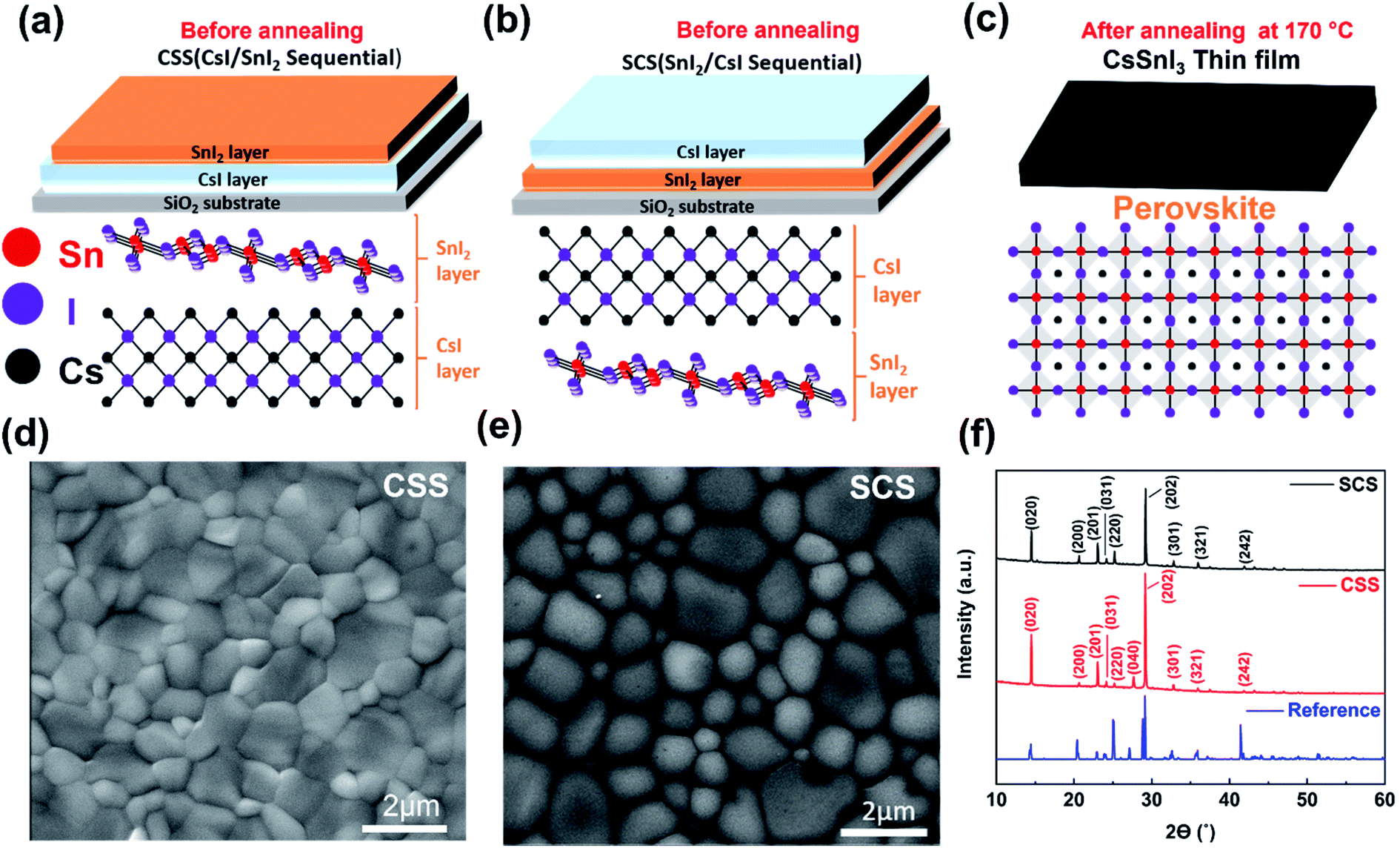 | ||
| Fig. 1 The deposition methods, morphology and crystal structure of CsSnI3 thin films with two different deposition methods. (a–c) Schematics of CsSnI3 thin films deposition of CsI/SnI2 sequential (CSS) and SnI2/CsI sequential (SCS) methods, respectively (before and after annealing steps). (d and e) SEM images of CSS and SCS CsSnI3 thin films after annealing. (f) XRD patterns of two types and ref. 30 CsSnI3 thin films with lattice plane indices. | ||
To understand the stability of our films, we performed time-dependent UV-vis absorption at ten minute intervals for 10 hours. It is evident from the reduced rate of quenching of the main absorbance peaks of the pristine films (Fig. 2a and b) that the SCS film is much more stable in air than the CSS film. To compare their air stability more quantitatively, we compared the absorbance of both films at 420 nm (Fig. 2c). The normalized absorbance of SCS and CSS films decreased to 86% and 37% of their initial values in the first 5 hours, respectively. After 10 hours these values were 73% for the SCS films and 24% for CSS film. This indicates a substantial improvement in stability for SCS films compared to CSS films despite only modest differences observed in the morphology. Previous work has demonstrated that certain additives, such as SnX2 (X = F−, Cl− and Br−) can suppress Sn2+ oxidation and increase the air stability of Sn-based halide perovskites through their Sn2+-rich conditions, the sequestration of Sn4+ by halides and the sacrificial role of SnX2.31,37–41 SnX2 has previously been introduced into the synthesis of CsSnI3 films with the result that F− and Cl− doped CsSnI3 thin films kept 50% and 70% of their absorbance at 420 nm respectively after 120 minutes air exposure,31 much more than the 30% retained by undoped films after the same duration of air exposure. The ambient humidity has also been reported to play a significant role in the degradation of Sn-based halide perovskites.42 Haque et al. reported that (PEA)0.2(FA)0.8SnI3 films presented more pronounced optical degradation when oxidised in air with increased humidity.43 In addition, the absorbance of thermally evaporated CsSnI3−xClx thin films deposited by Liu et al.26 remained at 70% of the initial value after 500 minutes air exposure. However, the absorbance of our films, retaining 73% of absorbance at 420 nm after 600 minutes air exposure, occurs just by adjustment of the deposition procedure without using a mixed anion composition.
 | ||
| Fig. 2 UV-vis absorption spectra and electrical conductivity of two types CsSnI3 thin films. (a and b) Time dependent (10 hours) UV-vis absorption spectra of SCS and CSS CsSnI3 thin films. (c) Normalized time dependent absorbance at 420 nm for CsSnI3 films formed via SCS and CSS methods. (d and e) Time dependent electrical conductivity of SCS and CSS CsSnI3 thin films in nitrogen atmosphere and in air (20 °C, 20% RH). | ||
To further understand the stability of our films, we performed time-dependent electrical conductivity measurements both in inert atmosphere (N2 glovebox, H2O < 0.1 ppm and O2 < 0.1 ppm) and in air (Fig. 2d and e). When tested in inert conditions, the initial electrical conductivity of SCS and CSS films increases with time over a 60 minute period from initial values of 1.2 S cm−1 and 1.6 S cm−1, respectively. The rate of increase is substantially higher for CSS films. In the first minute of air exposure, the electrical conductivity of both films jumps by a factor of ∼10 due to the oxidation of Sn2+ to Sn4+. After 60 minutes air exposure, the conductivity of CSS films had decreased significantly to <7% of the peak value. In the case of SCS films, the conductivity was at ∼88% of the peak value after 60 minutes in air. The SCS films therefore show a higher electrical stability in both N2 and air atmosphere, which may be attributed to the slightly larger grain size or a more suitable film morphology. A further possibility is a compositional gradient in the films, which will be explored later in this manuscript.
To confirm the impact of oxidation on the thermoelectric properties of CsSnI3, we performed thermoelectric property measurements (293–353 K) for both films with time dependent air exposure at 20 °C (Fig. S4†) and 80 °C (Fig. 3), respectively. For SCS films, the initial electrical conductivity, σ0, was 15.4 ± 1 S cm−1 at 20 °C (noting that there is air exposure for ∼1 minute during transfer from the nitrogen glove box to the analysis instrument where it is pumped down to vacuum). When exposing them to air at 20 °C (3 minutes at a time), the conductivity increased steadily to 37.2 S cm−1 after 15 minutes (σ15min/20°C) (Fig. S4a†). However, when exposing them to air at 80 °C, the electrical conductivity value grew more rapidly to 88.2 ± 8.3 S cm−1 (σ9min/80°C) after 9 minutes exposure, before decreasing to 74.4 ± 4.4 S cm−1 after 15 minutes (σ15min/80°C) (Fig. 3a). For CSS films, the initial electrical conductivity σ0 was 13.2 ± 2 S cm−1 (σ0) and this increased to 38.3 S cm−1 (σ15min/20°C) after 15 minutes of air exposure at 20 °C (Fig. S4d†), which is a similar trend compare to SCS film. Nonetheless, the CSS film shows a higher electrical conductivity than that of SCS film when they are oxidised at 80 °C. Its value increases dramatically to 98.4 ± 16 S cm−1 (σ12min/80°C) after 12 minutes, before decreasing to 94 ± 17 S cm−1 after 15 minutes (σ15min/80°C) (Fig. 3d). This trend in electrical conductivity for CsSnI3 in air which initially increases sharply before decaying, has been reported previously26 and is due to the competition between charge carrier concentration increasing and carrier mobility decreasing during oxidation. However, here we found that temperature plays a significant role in the oxidation rate of Sn2+ to Sn4+ and that higher electrical conductivities are achieved when the oxidation is done at a higher temperature. The Seebeck coefficient, S, of both films (Fig. 3b, e, S4b and e†) shows a positive trend with temperature in the range 293–353 K, but steadily decreases with air exposure. The positive sign of the Seebeck coefficient confirms that holes are the dominant charge carriers in both films. For SCS films, the initial Seebeck coefficient (S0 at 20 °C) is 124 ± 7.2 μV K−1 and reduces by just 13% to 107.9 μV K−1 (S15min/20°C) after 15 minutes air exposure at 20 °C (Fig. S4b†). However, its Seebeck coefficient reduces by ∼40% to 74 ± 4.4 μV K−1 (S15min/80°C) after air exposure at 80 °C for the same amount of time (Fig. 3b). Because the Seebeck coefficient is inversely related to the charge carrier density, this is evidence of self-doping by Sn2+ to Sn4+ oxidation during air exposure, which occurs at a higher rate at elevated temperatures. For the CSS film. Its initial Seebeck coefficient (S0) is 127.4 ± 11 μV K−1 at 20 °C, which reduces 19% to 103 μV K−1 (S15min/20°C) and 53% to 60 ± 6.3 μV K−1 (S15min/80°C) after 15 minutes air exposure at 20 °C and 80 °C (Fig. S4e† and 3e), respectively. This indicates a slightly faster rate of self-doping by Sn2+ to Sn4+ oxidation in the CSS films, in line with the more rapid degradation in optical and electronic properties seen in Fig. 2.
 | ||
| Fig. 3 Thermoelectric properties of two types CsSnI3 thin films oxidised at 80 °C. Temperature dependent electrical conductivity, σ (a), Seebeck coefficient, S (b), thermal conductivity, κtotal (c), power factor, PF (g) and figure-of-merit, zT (i), of SCS CsSnI3 thin films with air exposure at 80 °C. Temperature dependent electrical conductivity, σ (d), Seebeck coefficient, S (e), thermal conductivity, κtotal (f), power factor, PF (h) and figure-of-merit, zT (j) of CSS CsSnI3 thin films with air exposure at 80 °C. | ||
Fig. 3c, f, S4(c) and (f)† show the temperature dependent thermal conductivity of SCS and CSS films oxidised at 80 °C and 20 °C. The initial thermal conductivities of SCS and CSS films are 0.29 ± 0.01 W m−1 K−1 and 0.33 ± 0.01 W m−1 K−1 at 20 °C, respectively. In the case of air exposure at 20 °C, the thermal conductivity of both films changes very little, remaining in the range 0.29 W m−1 K−1 to 0.30 W m−1 K−1 for SCS films and 0.32 W m−1 K−1 to 0.34 W m−1 K−1 for CSS films, respectively. However, in the case of air exposure at 80 °C, both films show a large growth of thermal conductivity to maxima of 0.34 ± 0.01 W m−1 K−1 and 0.43 ± 0.01 W m−1 K−1 for SCS and CSS films, respectively. To understand the reason for the significant growth of thermal conductivity for both films after air exposure at 80 °C, we plotted the total thermal conductivity (κtotal = κelectronic + κlattice) as a function of electrical conductivity (σ) for both films (Fig. S5 and S6†). We then fitted the experimental data to the Wiedemann–Franz law (κelectronic = σLT), keeping the Lorenz number as a free parameter (Fig. S5d and S6d†). This analysis assumes that the lattice thermal conductivity of both films is constant when electrical conductivity increases. We found the lattice thermal conductivity of SCS and CSS films to be 0.28 ± 0.01 W m−1 K−1 and 0.32 ± 0.01 W m−1 K−1 at room temperature, respectively, which is marginally lower than the literature.24,26 We then calculated the average Lorenz number of SCS (2.55 ± 0.6 × 10⁻⁸ W Ω K−2) and CSS films (3.51 ± 1.3 × 10⁻⁸ W Ω K−2) over the whole temperature range. The average Lorenz numbers of SCS films agree with the Sommerfeld value (2.40 × 10⁻⁸ W Ω K−2), within their error bars, which suggests that the total thermal conductivity growth of SCS films after air exposure at 80 °C is due to the increase of κelectronic caused by self-doping.
The power factor, PF of both films (Fig. S4(g) and (h)†) shows a continuous growth with air exposure at 20 °C, obtaining the maximum value of 0.45 μW cm−1 K−2 at 313 K for SCS films and 0.41 μW cm−1 K−2 at 303 K for CSS films. However, in case of air exposure at 80 °C, the PF of SCS films (Fig. 3g and h increases significantly to the highest number of 0.69 μW cm−1 K−2 at 333 K (PF3min/80°C) after the first 3 minute air exposure and then constantly reduces. For CSS films, its highest PF number of 0.62 μW cm−1 K−2 is achieved at 333 K (PF6min/80°C) after the second 3 minute air exposure. Finally, we calculated the temperature dependent figure of merit, zT, for both films, shown in Fig. 3i, j, S4(i) and (j).† When the air exposure temperature is 20 °C, the maximum zT at 323 K is 0.052 (zT15min/20°C) and 0.041 (zT6min/20°C) for SCS and CSS films, respectively (Fig. S4(i) and (j)†). We note that due to the relative stability of the SCS films at 20 °C, zT has not reached a clear maximum on this timescale. However, when exposing them to air at 80 °C, the highest zT is 0.08 ± 0.01 for SCS and 0.06 ± 0.01 for CSS films, which is reached after 3 minutes for both films.
To understand the oxidation process of both films at room and higher temperature, we performed depth profile XPS measurement for films oxidised at room temperature and 80 °C. Our depth profiling showed that there was a concentration gradient in Sn and Cs through the thickness of the film. There was more Sn (30%) on the top surface for CSS films, and its concentration decreases gradually to the base of the film (10%). This indicates that the baking step had resulted in an incomplete reaction between the two precursor layers and that a concentration gradient related to the order of CsI and SnI2 deposition persists in the final films (Fig. S9†). The Sn2+ rich surface of CSS films should lead to more rapid Sn2+ oxidation to Sn4+ on the CSS film surface compared to the SCS case. This Sn2+ concentration gradient is the most likely explanation of the stability differences between SCS and CSS films. There is no significant change in the Cs 3d (Fig. S10†) and I 3d (Fig. S12†) peaks in the top 12 nm of the films after 5 minutes air exposure at 20 °C or 80 °C for both films. On the other hand (Fig. S13†), we found oxygen in the top 3 nm of CSS and SCS films exposed to air at 20 °C and in a thicker layer for CSS and SCS films that oxidised at 80 °C (where the oxygen had reduced to half the surface value at 6 nm and was still detectable at 12 nm depth). This is further evidence that temperature accelerates the oxidative self-doping of CsSnI3 films and confirms that this occurs from the surface to the bulk. In addition, there is a 0.8 eV shift of the Sn3d5/2 peak for both films upon oxidising at 80 °C (Fig. S11c and d†). To further understand the oxidation state of Sn, we performed Auger electron spectroscopy (AES). Fig. 4a and b displays the AES Sn MNN curves with fitted peaks (labelled a to d) as function of etching depth for SCS and CSS films that were each oxidised at 20 °C and 80 °C (fitting details shown in Table S1†). The peak positions in our spectra are in good agreement with the reported Auger spectrum of CsSnI3−xClx.26 According to the reported M4,5N4,5N4,5 Auger spectrum of tin and oxidised tin,44 the fitted peak a (1S0) is present in Sn metal and shows a large broadening after oxidation. In our CsSnI3 films, the 1S0 peak (fitted curve a) is broad in all cases, confirming the absence of Sn0 states. Peak c (1G41D2) is related to Sn4+ states45–47 and disappears at the etching depth of 6 nm for SCS and CSS films oxidised at 20 °C, and at 9 nm when oxidised at 80 °C (Fig. 4e and f). This confirms that the oxidised layer is thicker when the oxidation occurs at a higher temperature, in agreement with our observations of the O 1s peak. To clearly compare the Sn states for each depth of our films, we calculated the modified Auger parameters (α′) and depicted the data as Wagner plots (Fig. 4g). For a given chemical state, α′ is defined as the sum of the binding energy of the core electrons (Eb) and the kinetic energy of the corresponding Auger electrons (Ek), α′ = Eb + Ek,48 and is insensitive to sample charging effects. The Wagner plot (Fig. 4g) shows the photoelectron binding energies, Auger-electron kinetic energies and modified Auger parameters of Sn in our films (full details in Table S2†) as a function of etching depth and compares these to reference values.46,47 The majority Sn4+ states at the surface give way gradually to Sn2+ states over a depth range of 6 to 9 nm for oxidation at 20 °C and 80 °C alike, which further demonstrated high temperature driven oxidation processes of CsSnI3. The films oxidised at 80 °C have more Sn4+ character in these surface layers, and the CSS surface layers have more Sn4+ character than the SCS films, in line with our other XPS, optical, electronic and thermoelectric characterisation.
 | ||
| Fig. 4 Auger electron spectra (AES) of Sn MNN of two types CsSnI3 thin films. (a–d) AES (etching from 0 nm to 12 nm) of SCS and CSS which oxidised at 20 °C and 80 °C, respectively. (e and f) Photoelectron counts of fitted curves in (a–d). (g) Chemical state plot with modified Auger parameter for Sn compounds (Sn, Sn2+ and Sn4+) and our measurements (the point of SCS and CSS that oxidised at 80 °C coincides at 0 nm). | ||
Conclusions
In summary, we propose a new perspective to thermal evaporation of CsSnI3 thin films by tuning the sequence of precursor deposition. We demonstrate the impact of thermal vapour deposition sequence on their surface morphology, conductivity and air stability. The SCS films show a slightly larger grain size and their optical and electrical properties show significantly higher air stability compared to the CSS films. We further studied the thermoelectric properties of both sequential films as a function of air exposure time and oxidation temperature. Both films show relatively stable thermoelectric properties when exposing them to air at 20 °C. The electrical conductivity, Seebeck coefficient and thermal conductivity change slowly with further air exposure. The thermoelectric properties of the films oxidised at 80 °C show larger changes in their thermoelectric properties as a function of oxidation time. Their electrical conductivity and thermal conductivity increase significantly at the onset of oxidation, with a concomitant decrease of Seebeck coefficient. A maximum zT for partially oxidised films of 0.08 is reached. Our work indicates that the mechanism of self-doping CsSnI3 thin films is from surface to bulk and is significantly accelerated by modest increases in temperature. Oxygen appears only at the surface and is not present in measurable quantities beyond 6 nm depth for films oxidised room temperature and 9 nm for films oxidised at higher temperature for the oxidation times studied. Moreover, our AES data shows a gradual shift from Sn4+ states at the surface to Sn2+ states in the bulk, with the fitted peak c that is related to the presence of Sn4+ states disappearing at a depth of 6 nm for films oxidised at 20 °C and a depth of 9 nm deep for films oxidised at 80 °C. The average Lorenz number of SCS films over the full temperature range shows a value similar to the Sommerfeld value.26 This work has described a strategy for CsSnI3 thin film thermal deposition with enhanced air stability which may be applicable for many devices built around Pb-free halide perovskites. The thermoelectric performance of these more stable films is comparable with the state-of-the-art for halide perovskites and reveals an impact of oxidation temperature on CsSnI3 thermoelectric performance.Author contributions
WT and TL performed the deposition of CsSnI3 films. WT performed experimental work and data analysis. This project was conceived and planned by OF and WT and supervised by OF. The paper was written by WT with input from all authors.Conflicts of interest
There are no conflicts to declare.Acknowledgements
W. Tang and T. Liu thank the China Scholarship Council (CSC) for funding. OF is funded by a Royal Society University Research Fellowship (UF140372 and URF/R/201013).References
- Net zero emissions race 2020 scorecard, accessed Feb 27, 2021, https://eciu.net/netzerotracker.
- R. Zevenhoven and A. Beyene, Energy, 2011, 36, 3754–3762 CrossRef.
- D. Champier, Energy Convers. Manage., 2017, 140, 167–181 CrossRef.
- Q. Zhang, Y. Sun, W. Xu and D. Zhu, Adv. Mater., 2014, 26, 6829–6851 CrossRef CAS PubMed.
- NREL Best Research-Cell Efficiency, accessed 04/10/2020, https://www.nrel.gov/pv/assets/pdfs/best-research-cell-efficiencies.20200104.pdf.
- X. Zhao, C. Yao, K. Gu, T. Liu, Y. Xia and Y.-L. Loo, Energy Environ. Sci., 2020, 13, 4334–4343 RSC.
- X. Zhao, C. Yao, T. Liu, J. C. Hamill Jr, G. O. Ngongang Ndjawa, G. Cheng, N. Yao, H. Meng and Y.-L. Loo, Adv. Mater., 2019, 31, 1904494 CrossRef CAS PubMed.
- M. Kim, J. Jeong, H. Lu, K. Lee Tae, T. Eickemeyer Felix, Y. Liu, W. Choi, J. Choi Seung, Y. Jo, H.-B. Kim, S.-I. Mo, Y.-K. Kim, H. Lee, G. An Na, S. Cho, R. Tress Wolfgang, M. Zakeeruddin Shaik, A. Hagfeldt, Y. Kim Jin, M. Grätzel and S. Kim Dong, Science, 2022, 375, 302–306 CrossRef CAS PubMed.
- M. A. Green, A. Ho-Baillie and H. J. Snaith, Nat. Photonics, 2014, 8, 506–514 CrossRef CAS.
- S. D. Stranks and H. J. Snaith, Nat. Nanotechnol., 2015, 10, 391–402 CrossRef CAS PubMed.
- S. D. Stranks, G. E. Eperon, G. Grancini, C. Menelaou, M. J. P. Alcocer, T. Leijtens, L. M. Herz, A. Petrozza and H. J. Snaith, Science, 2013, 342, 341 CrossRef CAS PubMed.
- X.-K. Liu, W. Xu, S. Bai, Y. Jin, J. Wang, R. H. Friend and F. Gao, Nat. Mater., 2021, 20, 10–21 CrossRef CAS PubMed.
- H. Zhu, Y. Fu, F. Meng, X. Wu, Z. Gong, Q. Ding, M. V. Gustafsson, M. T. Trinh, S. Jin and X. Y. Zhu, Nat. Mater., 2015, 14, 636–642 CrossRef CAS PubMed.
- T. Liu, W. Tang, S. Luong and O. Fenwick, Nanoscale, 2020, 12, 9688–9695 RSC.
- F. Yuan, X. Zheng, A. Johnston, Y.-K. Wang, C. Zhou, Y. Dong, B. Chen, H. Chen, J. Z. Fan, G. Sharma, P. Li, Y. Gao, O. Voznyy, H.-T. Kung, Z.-H. Lu, O. M. Bakr and E. H. Sargent, Sci. Adv., 2020, 6, eabb0253 CrossRef CAS PubMed.
- Y. He and G. Galli, Chem. Mater., 2014, 26, 5394–5400 CrossRef CAS.
- Y.-K. Jung, I. T. Han, Y. C. Kim and A. Walsh, npj Comput. Mater., 2021, 7, 51 CrossRef CAS.
- M. A. Haque, M. I. Nugraha, S. H. K. Paleti and D. Baran, J. Phys. Chem. C, 2019, 123, 14928–14933 CrossRef CAS.
- Q. Liu, Y.-C. Hsiao, M. Ahmadi, T. Wu, L. Liu, S. Haacke, H. Wang and B. Hu, Org. Electron., 2016, 35, 216–220 CrossRef CAS.
- W. Tang, J. Zhang, S. Ratnasingham, F. Liscio, K. Chen, T. Liu, K. Wan, E. S. Galindez, E. Bilotti, M. Reece, M. Baxendale, S. Milita, M. A. McLachlan, L. Su and O. Fenwick, J. Mater. Chem. A, 2020, 8, 13594–13599 RSC.
- M. A. Haque, S. Kee, D. R. Villalva, W.-L. Ong and D. Baran, Adv. Sci., 2020, 7, 1903389 CrossRef CAS PubMed.
- X. Mettan, R. Pisoni, P. Matus, A. Pisoni, J. Jaćimović, B. Náfrádi, M. Spina, D. Pavuna, L. Forró and E. Horváth, J. Phys. Chem. C, 2015, 119, 11506–11510 CrossRef CAS.
- R. Heiderhoff, T. Haeger, N. Pourdavoud, T. Hu, M. Al-Khafaji, A. Mayer, Y. Chen, H.-C. Scheer and T. Riedl, J. Phys. Chem. C, 2017, 121, 28306–28311 CrossRef CAS.
- W. Lee, H. Li, A. B. Wong, D. Zhang, M. Lai, Y. Yu, Q. Kong, E. Lin, J. J. Urban, J. C. Grossman and P. Yang, Proc. Natl. Acad. Sci., 2017, 114, 8693 CrossRef CAS PubMed.
- C. Ge, M. Hu, P. Wu, Q. Tan, Z. Chen, Y. Wang, J. Shi and J. Feng, J. Phys. Chem. C, 2018, 122, 15973–15978 CrossRef CAS.
- T. Liu, X. Zhao, J. Li, Z. Liu, F. Liscio, S. Milita, B. C. Schroeder and O. Fenwick, Nat. Commun., 2019, 10, 5750 CrossRef CAS PubMed.
- A. Walsh, D. O. Scanlon, S. Chen, X. G. Gong and S.-H. Wei, Angew. Chem., Int. Ed., 2015, 54, 1791–1794 CrossRef CAS PubMed.
- R. E. Brandt, V. Stevanović, D. S. Ginley and T. Buonassisi, MRS Commun., 2015, 5, 265–275 CrossRef CAS.
- Y. Takahashi, H. Hasegawa, Y. Takahashi and T. Inabe, J. Solid State Chem., 2013, 205, 39–43 CrossRef CAS.
- I. Chung, J.-H. Song, J. Im, J. Androulakis, C. D. Malliakas, H. Li, A. J. Freeman, J. T. Kenney and M. G. Kanatzidis, J. Am. Chem. Soc., 2012, 134, 8579–8587 CrossRef CAS PubMed.
- K. P. Marshall, M. Walker, R. I. Walton and R. A. Hatton, Nat. Energy, 2016, 1, 16178 CrossRef CAS.
- T. Liu, S.-Y. Yue, S. Ratnasingham, T. Degousée, P. Varsini, J. Briscoe, M. A. McLachlan, M. Hu and O. Fenwick, ACS Appl. Mater. Interfaces, 2019, 11, 47507–47515 CrossRef CAS PubMed.
- V. Linseis, F. Völklein, H. Reith, K. Nielsch and P. Woias, Rev. Sci. Instrum., 2018, 89, 015110 CrossRef CAS PubMed.
- S. Saini, A. K. Baranwal, T. Yabuki, S. Hayase and K. Miyazaki, J. Electron. Mater., 2020, 49, 2890–2894 CrossRef CAS.
- T.-B. Song, T. Yokoyama, S. Aramaki and M. G. Kanatzidis, ACS Energy Lett., 2017, 2, 897–903 CrossRef CAS.
- T.-B. Song, T. Yokoyama, J. Logsdon, M. R. Wasielewski, S. Aramaki and M. G. Kanatzidis, ACS Appl. Energy Mater., 2018, 1, 4221–4226 CrossRef CAS.
- T. Zhang, H. Li, H. Ban, Q. Sun, Y. Shen and M. Wang, J. Mater. Chem. A, 2020, 8, 4118–4124 RSC.
- M. Chen, M.-G. Ju, H. F. Garces, A. D. Carl, L. K. Ono, Z. Hawash, Y. Zhang, T. Shen, Y. Qi, R. L. Grimm, D. Pacifici, X. C. Zeng, Y. Zhou and N. P. Padture, Nat. Commun., 2019, 10, 16 CrossRef CAS PubMed.
- A. G. Kontos, A. Kaltzoglou, E. Siranidi, D. Palles, G. K. Angeli, M. K. Arfanis, V. Psycharis, Y. S. Raptis, E. I. Kamitsos, P. N. Trikalitis, C. C. Stoumpos, M. G. Kanatzidis and P. Falaras, Inorg. Chem., 2017, 56, 84–91 CrossRef CAS PubMed.
- K. J. Savill, A. M. Ulatowski, M. D. Farrar, M. B. Johnston, H. J. Snaith and L. M. Herz, Adv. Funct. Mater., 2020, 30, 2005594 CrossRef CAS.
- J. Pascual, M. Flatken, R. Félix, G. Li, S.-H. Turren-Cruz, M. H. Aldamasy, C. Hartmann, M. Li, D. Di Girolamo, G. Nasti, E. Hüsam, R. G. Wilks, A. Dallmann, M. Bär, A. Hoell and A. Abate, Angew. Chem., Int. Ed., 2021, 60, 21583–21591 CrossRef CAS PubMed.
- M. A. Haque, L. H. Hernandez, B. Davaasuren, D. R. Villalva, J. Troughton and D. Baran, Advanced Energy and Sustainability Research, 2020, 1, 2000033 CrossRef.
- L. Lanzetta, T. Webb, N. Zibouche, X. Liang, D. Ding, G. Min, R. J. E. Westbrook, B. Gaggio, T. J. Macdonald, M. S. Islam and S. A. Haque, Nat. Commun., 2021, 12, 2853 CrossRef CAS PubMed.
- S. Barlow, P. Bayat-Mokhtari and T. E. Gallon, J. Phys. C: Solid State Phys., 1979, 12, 5577–5584 CrossRef CAS.
- L. Kövér, G. Moretti, Z. Kovács, R. Sanjinés, I. Cserny, G. Margaritondo, J. Pálinkás and H. Adachi, J. Vac. Sci. Technol., A, 1995, 13, 1382–1388 CrossRef.
- A. F. Lee and R. M. Lambert, Phys. Rev. B, 1998, 58, 4156–4165 CrossRef CAS.
- L. Kövér, Z. Kovács, R. Sanjinés, G. Moretti, I. Cserny, G. Margaritondo, J. Pálinkás and H. Adachi, Surf. Interface Anal., 1995, 23, 461–466 CrossRef.
- M. Satta and G. Moretti, J. Electron Spectrosc. Relat. Phenom., 2010, 178–179, 123–127 CrossRef CAS.
Footnote |
| † Electronic supplementary information (ESI) available. See DOI: 10.1039/d1ta11093d |
| This journal is © The Royal Society of Chemistry 2022 |