
 Open Access Article
 This Open Access Article is licensed under a
 Creative Commons Attribution 3.0 Unported Licence
Solution-based synthesis of wafer-scale epitaxial BiVO4 thin films exhibiting high structural and optoelectronic quality†
Viktoria F.
Kunzelmann
 ,
Chang-Ming
Jiang
,
Irina
Ihrke
,
Elise
Sirotti
,
Tim
Rieth
,
Alex
Henning
,
Johanna
Eichhorn
and
Ian D.
Sharp
*
,
Chang-Ming
Jiang
,
Irina
Ihrke
,
Elise
Sirotti
,
Tim
Rieth
,
Alex
Henning
,
Johanna
Eichhorn
and
Ian D.
Sharp
*
Walter Schottky Institute and Physics Department, Technische Universität München, Am Coulombwall 4, 85748 Garching, Germany. E-mail: sharp@wsi.tum.de
First published on 22nd April 2022
Abstract
We demonstrate a facile approach to solution-based synthesis of wafer-scale epitaxial bismuth vanadate (BiVO4) thin films by spin-coating on yttria-stabilized zirconia. Epitaxial growth proceeds via solid-state transformation of initially formed polycrystalline films, driven by interface energy minimization. The (010)-oriented BiVO4 films are smooth and compact, possessing remarkably high structural quality across complete 2′′ wafers. Optical absorption is characterized by a sharp onset with a low sub-band gap response, confirming that the structural order of the films results in correspondingly high optoelectronic quality. This combination of structural and optoelectronic quality enables measurements that reveal a strong optical anisotropy of BiVO4, which leads to significantly increased in-plane optical constants near the fundamental band edge that are of particular importance for maximizing light harvesting in semiconductor photoanodes. Temperature-dependent transport measurements confirm a thermally activated hopping barrier of ∼570 meV, consistent with small electron polaron conduction. This simple approach for synthesis of high-quality epitaxial BiVO4, without the need for complex deposition equipment, enables a broadly accessible materials base to accelerate research aimed at understanding and optimizing photoelectrochemical energy conversion mechanisms.
Introduction
Ternary metal oxide semiconductors have attracted considerable interest as photoelectrode materials for the sustainable conversion of sunlight to chemical fuels. Within this class of compounds, monoclinic scheelite (ms-)bismuth vanadate (BiVO4) currently stands as the best performing photoanode material due to its moderate band gap of ∼2.5 eV, favorable band edge energetics, and ability to be stabilized in aqueous solutions.1–6 Despite the significant improvements in photoelectrochemical performance characteristics of BiVO4 in recent years, critical questions regarding the roles of polaron transport and recombination, bulk and interfacial defects, and surface chemical transformations on light-to-chemical energy conversion remain unanswered. With a few notable exceptions, most studies of BiVO4 have focused on polycrystalline or nanostructured thin films, the internal complexities of which have hindered mechanistic elucidation of these characteristics. Although additional insights have been enabled by studies of highly oriented thin films,7,8 minimization of structural disorder is necessary to enable better understanding of critical loss processes. To address this knowledge gap, epitaxial films can serve as important model systems. Until now, epitaxial BiVO4 films have primarily been synthesized via pulsed laser deposition (PLD),9–14 though molecular beam epitaxy (MBE)15 and chemical vapor deposition (CVD)16 processes have also been reported. While studies based on such samples have provided impactful insights into charge transport,17 energetics,18 and surface reactivity,19 these deposition methods require sophisticated experimental infrastructure and complex parameter optimization. As a consequence, only a handful of groups have succeeded in achieving heteroepitaxial thin films and, to the best of our knowledge, wafer-scale growth of high structural quality epitaxial BiVO4 by any method has not yet been reported. Thus, realization of scalable solution-based approaches for epitaxial growth are urgently needed to accelerate mechanistic understanding and rational development of materials for photoelectrochemical energy conversion.In this work, we introduce a new approach for wafer-scale synthesis of epitaxial ms-BiVO4 on yttria-stabilized zirconia (YSZ) (001) using a solution-based process comprising spin-coating, metalorganic decomposition, and solid-state epitaxial transformation. This technique allows facile fabrication of thin films possessing a high optoelectronic quality and a structural quality that exceeds previously reported epitaxial BiVO4 films produced using much more sophisticated deposition approaches, as exemplified by high-resolution X-ray diffraction (HR-XRD) measurements. We find that, compared to polycrystalline thin films, (010) BiVO4 is characterized by significantly increased band-edge optical constants due to the strong uniaxial anisotropy of the material, indicating the importance of orientation control on maximizing light absorption in photoelectrodes. More generally, this facile and scalable method for synthesizing epitaxial BiVO4 will enable widespread availability of highly ordered material required for elucidating physical and chemical mechanisms of photoelectrochemical energy conversion.
Experimental section
Synthesis procedure for BiVO4 thin films
Prior to deposition of BiVO4/YSZ, the two-inch (2′′) YSZ (001) wafer (8 mol% yttria, undoped, Alineason) was prepared by careful rubbing of the surface in acetone with clean room quality cleaning swabs, followed by cleaning in an ultrasonic bath, first for 10 min in acetone and subsequently for 10 min in isopropanol. The sample substrate was then dried under flowing N2. Afterwards, the YSZ wafer was placed on a 1 mm thick steel plate and pre-annealed at 500 °C for 30 min in air at ambient pressure in a muffle furnace (LT 3/12, Nabertherm). This pre-annealing step was found to increase the wettability of the BiVO4 precursor solution on the substrate, which enabled high homogeneity and coverage over the full 2′′ wafer scale. The contact angle (CA) measurements of the precursor solution on YSZ in Fig. S1† confirm the reduction of the CA from ∼9° for as-cleaned YSZ to an undeterminably low CA for the pre-annealed YSZ. This shows the immediate, uniform distribution of the precursor solution on the annealed YSZ surface caused by an improved wettability due to the annealing treatment, which is beneficial for the growth of a continuous BiVO4 layer.The BiVO4 precursor solution was prepared in a 1![[thin space (1/6-em)]](https://www.rsc.org/images/entities/char_2009.gif) :1 ratio from two separate solutions, one containing 0.2 M bismuth(III) nitrate pentahydrate (Bi(NO3)3·5H2O, Sigma-Aldrich) in acetylacetone (C5H8O2, Sigma-Aldrich) and the other containing 0.03 M vanadium(IV)-oxy acetylacetonate (OV(C5H7O2)2, Sigma Aldrich) in acetylacetone. Each solution was sonicated for 10 min, after which the solutions were mixed and the final precursor solution was sonicated for an additional 5 min. Finally, the prepared solution was filtered with a PET membrane filter (0.2 μm pore size, 15 mm diameter, Carl Roth) to ensure a clean and fully mixed precursor. A drop of 500 μl precursor solution was spin-coated on a YSZ wafer with an acceleration rate of 150 rpm s−1, a spin speed of 1000 rpm for 12 s, and a deceleration rate of 150 rpm s−1. Subsequently, the wafer was placed on a 1 mm thick steel plate and annealed at 500 °C for 10 min in air at ambient pressure in a muffle furnace (LT 3/12, Nabertherm). After annealing, the wafer was taken out of the oven to cool down to room temperature for 12 min. Repeating this growth sequence for nine layers resulted in an approximately 43 nm thick polycrystalline (poly-)BiVO4/YSZ thin film. To achieve an epitaxial, single-phase BiVO4 layer, the resulting film was annealed at 650 °C for 10 min in a confined air volume of approximately 600 mm3. The volume confinement in the muffle furnace was formed by placing a clean, thermally stable silicon wafer approximately 300 μm above the BiVO4/YSZ wafer, supported by other wafer pieces that still allowed external air to enter. The purpose of this confinement was to mitigate loss of volatile elements from the surface during the annealing at 650 °C, thereby enabling a stoichiometric film to be retained. This configuration may have also reduced convective air flow over the surface, thereby improving temperature uniformity during the annealing treatment.
:1 ratio from two separate solutions, one containing 0.2 M bismuth(III) nitrate pentahydrate (Bi(NO3)3·5H2O, Sigma-Aldrich) in acetylacetone (C5H8O2, Sigma-Aldrich) and the other containing 0.03 M vanadium(IV)-oxy acetylacetonate (OV(C5H7O2)2, Sigma Aldrich) in acetylacetone. Each solution was sonicated for 10 min, after which the solutions were mixed and the final precursor solution was sonicated for an additional 5 min. Finally, the prepared solution was filtered with a PET membrane filter (0.2 μm pore size, 15 mm diameter, Carl Roth) to ensure a clean and fully mixed precursor. A drop of 500 μl precursor solution was spin-coated on a YSZ wafer with an acceleration rate of 150 rpm s−1, a spin speed of 1000 rpm for 12 s, and a deceleration rate of 150 rpm s−1. Subsequently, the wafer was placed on a 1 mm thick steel plate and annealed at 500 °C for 10 min in air at ambient pressure in a muffle furnace (LT 3/12, Nabertherm). After annealing, the wafer was taken out of the oven to cool down to room temperature for 12 min. Repeating this growth sequence for nine layers resulted in an approximately 43 nm thick polycrystalline (poly-)BiVO4/YSZ thin film. To achieve an epitaxial, single-phase BiVO4 layer, the resulting film was annealed at 650 °C for 10 min in a confined air volume of approximately 600 mm3. The volume confinement in the muffle furnace was formed by placing a clean, thermally stable silicon wafer approximately 300 μm above the BiVO4/YSZ wafer, supported by other wafer pieces that still allowed external air to enter. The purpose of this confinement was to mitigate loss of volatile elements from the surface during the annealing at 650 °C, thereby enabling a stoichiometric film to be retained. This configuration may have also reduced convective air flow over the surface, thereby improving temperature uniformity during the annealing treatment.
For reference measurements of polycrystalline BiVO4 on fused silica, wafers of fused silica (T24003, Siegert Wafer) with a diameter of 10 cm were rinsed with isopropanol and carefully scrubbed with a cleaning swab in a detergent solution (Alconox, Alconox Ing.). After rinsing with deionized water, the wafer was treated in an ozone cleaner for 10 min (UVC-1014, NanoBioAnalytics). The precursor preparation and spin-coating procedure were similar to the ones described above for the BiVO4/YSZ films, except that 1 ml precursor solution per layer was used, the wafer was placed on a 1 mm thick aluminum plate, and a final 2 h anneal was performed at 500 °C, as previously reported in the literature.20
Material characterization
Crystallographic characterization was performed using an X-ray diffractometer (SmartLab, Rigaku) equipped with a Cu anode and a 2-bounce Ge (220) monochromator. Out-of-plane θ–2θ scans were done between 2θ = 28–37° with 0.005° steps, with 1.0 mm incident/receiving slit sizes in the longitudinal direction. The rocking curves of the BiVO4 (040) reflection were measured with reduced 0.2 mm slit sizes to achieve better resolution. Azimuthal φ-scans were performed in asymmetric geometry: for the YSZ (204) reflection the incident and diffraction angles were respectively set as 68.67° and 15.54° relative to the sample surface (2θ = 84.21°). For the BiVO4 (082) reflection the incident and diffraction angles were 81.12° and 3.72°, respectively (2θ = 84.84°). Two-dimensional reciprocal space maps were collected with a point-like, non-monochromatic Cu X-ray source and a CCD detector (HyPix-3000, Rigaku) without any receiving optics; the sample tilting angle χ was varied between −5° and 70°. For grazing-incidence X-ray diffraction, no monochromator was used and the X-ray incident angle was fixed at 0.5°. The 2θ angle was then scanned between 10° and 70°. For the thickness determination of the epitaxial (epi-)BiVO4/YSZ, the interference oscillations around the BiVO4 (040) reflection were fit with a pseudo-Voigt function with a constant background (Fig. S2b†).Raman spectra were obtained with a home-built setup with a 532 nm wavelength laser (Torus 532, Laser Quantum). Prior to measurement, the system was calibrated to the 520 cm−1 peak of a single-crystal silicon reference. The backscattered light was analyzed with a spectrometer (iHR5500, HORIBA Scientific) equipped with a 2400 mm−1 grating and a CCD detector (Symphony II, HORIBA Scientific).
X-ray photoelectron spectroscopy data were recorded with a Kratos Axis Ultra setup equipped with a monochromatic Al Kα X-ray source and an applied power of 225 W. To avoid surface charging, charge neutralization was performed with the Kratos Axis electron charge neutralization system with an applied filament current of 0.45 A, a filament bias voltage of 1 V, and a charge balance voltage of 3 V. The survey spectra were measured with a pass energy of 160 eV and a step size of 1 eV, and the core level spectra were obtained with a pass energy of 10 eV and a step size of 0.03 eV. Remaining charging artifacts prevent detailed spectral fitting of individual components.
For the investigation of the bulk composition of the epitaxial BiVO4 films, a Bruker XFlash6130 energy-dispersive X-ray spectrometer, mounted in a Zeiss EVO MA10 for sample alignment imaging, was used. The EDX detection spot size was 1 μm and an electron beam energy of 20 keV was applied. The resulting spectra were analyzed using series fit deconvolution and the Phi-Rho-Z quantification mode.
A Bruker MultiMode 8 atomic force microscope was used for the topography measurements. All measurements were acquired in tapping mode with NSG30 tips (NT-MDT). The images were post-processed with the Bruker Nanoscope Analysis software with 0th order flattening and a 3rd order plane fit to account for instrumental aberrations. Prior to recording the high-resolution and cross-sectional scanning electron microscopy (SEM) images, a ∼3 nm thin carbon coating was sputtered on the investigated BiVO4 films to reduce charging. For the cross-sectional SEM images, the samples were then freshly cleaved to obtain a sharp edge. The SEM images were obtained with an NVision 40 FIB-SEM from Carl Zeiss using the secondary electron detector and an electron beam acceleration voltage of 2.0 kV.
Characterization of optical properties
The absorption coefficient was measured as a function of the photon energy with a home-built photo-thermal deflection setup. In Fig. S3† Tauc analysis was performed on the recorded absorption data to determine the indirect and direct band gap of the epi-BiVO4/YSZ and the BiVO4/fused silica. The optical transitions can be described by the following equation:| (αhν)n = A(hν − Eg) |
The optical constants of the BiVO4 films on YSZ and on fused silica were measured with a variable-angle spectroscopic ellipsometer from J. A. Wollam under a light incidence angle of 55°, 60° and 65°. The refractive index, n, the extinction coefficient, κ (Fig. S4a and c†), and the real, ε1, and imaginary, ε2, parts of the dielectric constant (Fig. S4b and d†) were obtained by fitting the spectroscopic ellipsometry data with a layer model developed with the CompleteEASE software from J. A. Wollam. The YSZ substrate was fit with a B-spline model with a fixed thickness of 0.5 mm and a Bruggeman effective medium approximation surface layer accounting for surface roughness. The B-spline layer was then parametrized as a general oscillator (GenOsc) layer consisting of a Cody–Lorentz oscillator including an Urbach absorption term to model absorption at energies below Eg, a Drude oscillator describing free carrier effects on the dielectric response, and a Gaussian oscillator, all fulfilling Kramers–Kronig consistency. For the fused silica substrate, the model as described by Philipp22 and found in the CompleteEASE database was used. The BiVO4 film was modelled as an additional B-spline layer on the YSZ substrate which was parametrized by a GenOsc layer with a three oscillator model as described by Cooper et al.,6 with: a Cody–Lorentz oscillator for modelling the indirect band gap of BiVO4, including parameters describing the Urbach tail associated with sub-band gap absorption induced by disorder, a PSemi-M0 oscillator for modeling the direct electronic transition in the semiconductor, and a PSemi-Tri oscillator to describe the remaining UV absorption.6
Solid-state conductivity measurements
For the in-plane DC conductivity measurements, Ti/Au (20/80 nm) interdigitated electrodes with a 10 μm spacing were evaporated on the BiVO4 surface with e-beam evaporation. The spacing of the interdigitated electrodes and the applied voltage were chosen so that the applied electric field |![[E with combining right harpoon above (vector)]](https://www.rsc.org/images/entities/i_char_0045_20d1.gif) | was within the low field approximation where the distortion caused by || is small in comparison to the transport barrier Eσ: || ≪ Eσ/e × d. Previous studies showed that polaron hopping is predicted to favorably occur between vanadium atoms23 so we overestimate the polaron hopping distance between two vanadium ions with d = 10 Å. Together with the assumption of a transport barrier of Eσ = 500 meV, as previously reported for undoped BiVO4,11 we obtain for the electric field: || ≪ 500 V μm−1.
| was within the low field approximation where the distortion caused by || is small in comparison to the transport barrier Eσ: || ≪ Eσ/e × d. Previous studies showed that polaron hopping is predicted to favorably occur between vanadium atoms23 so we overestimate the polaron hopping distance between two vanadium ions with d = 10 Å. Together with the assumption of a transport barrier of Eσ = 500 meV, as previously reported for undoped BiVO4,11 we obtain for the electric field: || ≪ 500 V μm−1.
Results
Solution-based synthesis approach for epitaxial BiVO4
In this study, we choose the conventional unit cell definition for ms-BiVO4 with a unique b-axis (a = 7.247 Å, b = 11.697 Å, c = 5.090 Å, β = 134.225°, Fig. S5†).24 Single crystal YSZ (001) was selected as the substrate since its cubic 5.145 Å lattice constant is well matched to the 5.094 Å and 5.196 Å V–V spacing in the BiVO4 (010) lattice planes to within 1%.25 We note that this YSZ substrate offers several advantages for fundamental studies of energy conversion processes. The transparent and insulating character enable precise characterization of optical properties and charge transport characteristics of the semiconductor absorber, respectively. Furthermore, YSZ is compatible with epitaxial growth of tin-doped indium oxide (ITO), which can eventually serve as an interfacial conductive back contact to epitaxial BiVO4.Cleaning and thermal pre-treatment of the YSZ wafer were performed to achieve high wettability, coverage, and homogeneity during the spin-coating process (Fig. S1†). The synthetic route to epi-BiVO4 layers (for complete details see Methods) is similar to the metalorganic decomposition method that has been previously used for fabrication of polycrystalline material.20,26 In brief, a precursor solution was mixed from two solutions containing 0.2 M bismuth(III) nitrate pentahydrate and 0.03 M vanadium(IV)-oxy acetylacetonate, each dissolved in acetylacetone. As shown in Fig. 1a, the precursor solution was then spin-coated onto a two-inch (2′′) YSZ (001) wafer and subsequently pyrolyzed at 500 °C for 10 min in a muffle furnace in ambient air. Repeating this growth sequence for nine layers resulted in an approximately 43 nm thick BiVO4 film with a polycrystalline structure, which was confirmed by grazing-incidence XRD (GI-XRD) (Fig. S2a†). To transform the polycrystalline films into epi-BiVO4, we performed a final annealing treatment at 650 °C for 10 min in ambient air. Raman spectroscopy confirms that the films comprise the monoclinic scheelite polymorph of BiVO4 both before and after this annealing treatment (Fig. S6†), as indicated by the (VO4)3−ν1 symmetric stretching mode at ∼826 cm−1.27
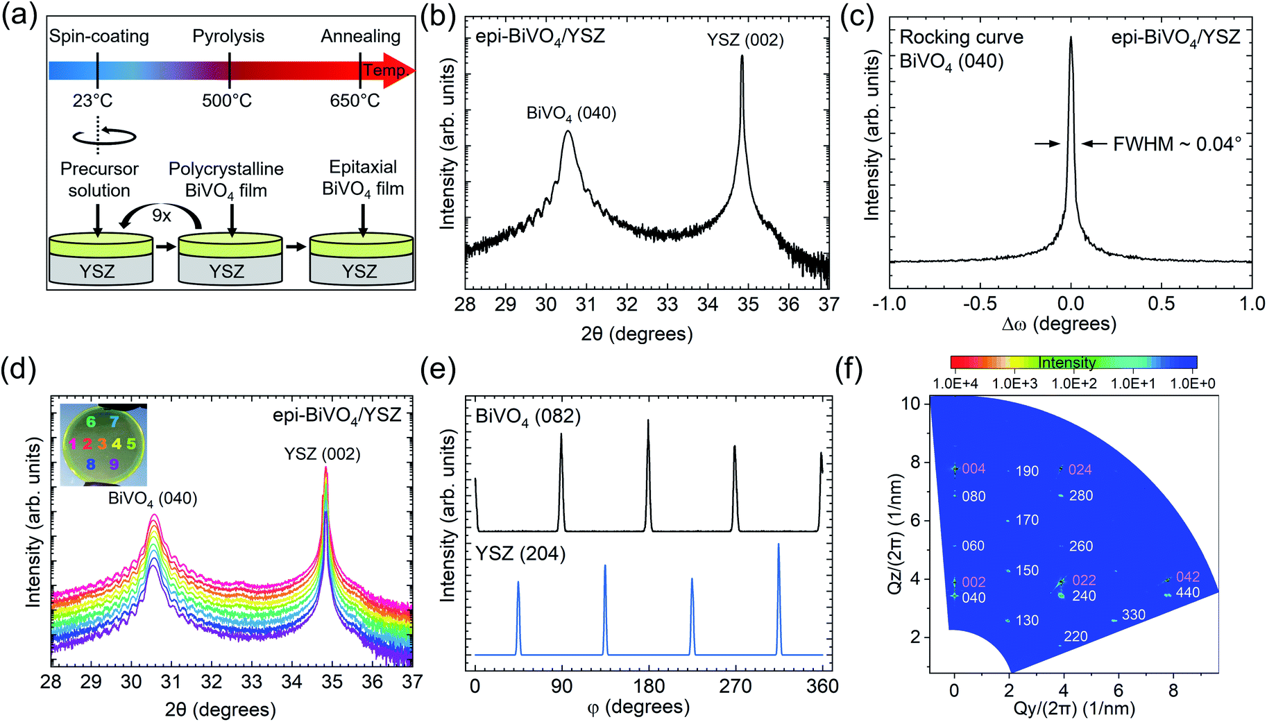 | ||
| Fig. 1 Illustration of synthesis procedure and structural characterization of epitaxial BiVO4/YSZ. (a) Schematic of the solution-based synthesis process of epi-BiVO4 on a complete 2′′ YSZ wafer, starting with spin-coating, followed by metalorganic decomposition to form a polycrystalline film, and a final annealing step at 650 °C to trigger the solid-state transformation into an epitaxial film. (b) High-resolution XRD θ–2θ scan of epi-BiVO4/YSZ. (c) Rocking curve recorded around the BiVO4 (040) peak at 2θ = 30.55°. (d) θ–2θ XRD scans of epi-BiVO4/YSZ at different measurement positions on the wafer (inset photo). (e) Azimuthal φ-scans of the epi-BiVO4 along the out-of-plane BiVO4 (082) and the YSZ (204) direction confirm the epitaxial relationship between the BiVO4 and the YSZ. (f) 2D reciprocal space map of the epi-BiVO4, with BiVO4 and YSZ peaks labelled in red and white, respectively. | ||
We note that this last annealing step is performed at a much higher temperature and for a shorter time than for the typical metalorganic decomposition approach for forming poly-BiVO4, which is usually carried out at 450–500 °C for several hours. This short time, high-temperature step is crucial for inducing a solid-state transformation of poly-BiVO4 into an epitaxial thin film, which will be discussed in detail below. We note that an advantage of this two-step method is that the epitaxial transformation is independent of the specific chemical route used to prepare the initial polycrystalline layer. Therefore, we expect this process to be broadly compatible with the various precursor solution compositions and solvents that have been reported for wet chemical synthesis of polycrystalline BiVO4 films.
At the high annealing temperature of 650 °C, it is known that vanadium becomes volatile in air.28 Therefore, this step was performed in a confined volume, which helped to maintain the desired stoichiometry. Consistent with prior reports of metalorganic decomposition-derived BiVO4,20,29 X-ray photoelectron spectroscopy (XPS) reveals a Bi-rich surface (Fig. S7†). The surface Bi:V ratio is found to be ∼1.7 for both the poly- and epi-BiVO4 films on YSZ, indicating that the combination of short time and spatial confinement during the 650 °C annealing step suppresses further volatilization of vanadium. Investigation of the bulk composition with energy-dispersive X-ray spectroscopy (EDX) revealed an atomic fraction of ∼48.4 at% bismuth and ∼51.6 at% vanadium (Fig. S8†). This bulk composition is consistent with the results of previous studies on similarly prepared polycrystalline thin films20 and confirms the 1:1 ratio between Bi and V in BiVO4 to within the few percent uncertainty of the EDX measurement.
Analysis of crystal structure and orientation
The crystallographic orientation and structural quality of the epi-BiVO4 films were analyzed using several XRD modes. Combining HR-XRD θ–2θ scans (Fig. 1b) and grazing-incidence 2θ scans (Fig. S2a†) indicates that the final 650 °C annealing step results in a transformation of the starting polycrystalline film into an epi-BiVO4 (010) film. Interference fringes surrounding the BiVO4 (040) Bragg peak arise from the high homogeneity and planarity of the film, with a period corresponding to a film thickness of ∼42.9 nm (Fig. S2b†). The observation of BiVO4 (020) and (060) reflections in extended-range θ–2θ scans (Fig. S2c†) confirms the monoclinic scheelite structure instead of the tetragonal scheelite phase. The structural quality of the epi-BiVO4 film was further quantified by analyzing the rocking curve of the BiVO4 (040) reflection at 30.55° (Fig. 1c). Remarkably, the rocking curve full width at half maximum (FWHM) of 0.04° is much lower compared to previous reports on epi-BiVO4 films grown on YSZ by PLD (0.097–0.3°)9–13 or CVD (0.13°).16 Importantly, this indicates that the facile spin-coating method reported here yields epi-BiVO4 films with a structural quality comparable to or exceeding that of material deposited by much more sophisticated systems, thereby providing a route to greatly increase availability of epitaxial layers within the research community.A key advantage of spin-coating is its potential for wafer-scale growth. To assess the growth homogeneity, a systematic series of θ–2θ scans was performed across the entire 2′′ YSZ wafer. At each measurement position, comparable diffractograms were observed (Fig. 1d) and the FWHMs of the corresponding BiVO4 (040) rocking curves are between 0.035° and 0.05° (Fig. S2d†). These measurements confirm the successful growth of a homogeneous, high-quality epi-BiVO4 (010) film over the entire surface of the YSZ (001) wafer and could be reliably reproduced in several epi-BiVO4/YSZ wafer growth runs (Fig. S9†). In addition, we performed ellipsometry measurements across the diameter of the epitaxial BiVO4 film, confirming a uniform thickness of approximately 43 nm (Fig. S10†). Edge effects that are common to spin-coating resulted in film thickening, but were limited to a 4 mm width around the circumference of the wafer.
The in-plane epitaxial relationship between BiVO4 and the YSZ substrate is revealed by azimuthal φ-scans of YSZ (204) and BiVO4 (082) reflections. As shown in Fig. 1e, both reflections exhibit a 4-fold symmetry and are offset by a ∼45° angle. Given the BiVO4 unit cell definition with a unique b-axis adopted in this work, its (082) reflection is expected to have a 2-fold symmetry. Therefore, the observed 4-fold symmetry is indicative of 90° in-plane twinning, with domains characterized by in-plane relationships of BiVO4 [001] ‖ YSZ [100] and BiVO4 [001] ‖ YSZ [010] (Fig. S11†). This assignment is further supported by 2D reciprocal space maps (RSM) with X-rays incident along the YSZ [100] direction (Fig. 1f). Not only does the pattern match with the simulated BiVO4 [001](010) ‖ YSZ [100](001) model (Fig. S12a†), but the (330), (440), and (260) BiVO4 reflections each exhibit a doublet feature caused by the 90° in-plane twinning. Similar conclusions can be drawn from the RSMs with X-rays incident along the YSZ [110] and [010] directions, as shown in Fig. S12b and c.†
Here, it is important to recognize that BiVO4 adopts the more symmetric tetragonal scheelite structure at the temperature used for the conversion of polycrystalline to epitaxial films and undergoes a second-order ferroelastic transformation to the monoclinic structure upon cooling.30,31 Therefore, azimuthal twinning occurs during cooling, after the out-of-plane epitaxial relationship has been established, and multi-domain films are commonly observed for epitaxial BiVO4 (010) on YSZ.9,15,32 Although single domain epitaxial BiVO4 (010) films have been claimed by a few groups,10–12,14 the experimental evidence for single domain films remains limited.
Elucidating the solid-state epitaxial transformation mechanism
To gain further insights into the solid-state epitaxial transformation and characteristics of the synthesized films, the surface morphologies of BiVO4 on YSZ were determined by atomic force microscopy (AFM) and scanning electron microscopy (SEM). Prior to the final high-temperature treatment, the polycrystalline film is characterized by a fine grain structure with a root mean square (rms) roughness of 5.2 nm (Fig. 2a). Annealing at 650 °C leads to the emergence of flat terraces with a size ranging from several hundred nm up to few μm, reducing the rms roughness to 3.3 nm (Fig. 2b). Over larger scales, plan view SEM images confirm that the BiVO4 layer is smooth and closed, as shown in Fig. 2c and d. This homogeneous coverage is confirmed by XPS measurements, in which no Zr or Y core level peaks from the substrate are detected (Fig. S7†). Cross-sectional SEM images (Fig. 2d) show an approximately uniformly thick and compact BiVO4 thin film with an average thickness of 42.8 nm. We note that epitaxial growth of compact BiVO4 films on YSZ can be achieved by PLD, but is challenging since islands usually form,9,10,13 most likely driven by the unknown energetics of the tetragonal scheelite BiVO4/YSZ interface during growth. In the present work, we also observe the formation of small particles when a single pyrolysis step is performed at 650 °C (Fig. S13a†). By contrast, a smoother polycrystalline layer forms at the optimized pyrolysis temperature of 500 °C (Fig. S13b†). Therefore, the two-step process is optimized to ensure compact and planar epitaxial films, while suppressing island formation. | ||
| Fig. 2 Morphological analysis of BiVO4/YSZ before and after the solid-state transformation. AFM topography images of (a) poly-BiVO4/YSZ starting material and (b) epi-BiVO4/YSZ after annealing at 650 °C. (c and d) Top-view SEM and (e) cross-sectional SEM images of epi-BiVO4/YSZ. | ||
Both AFM and SEM images reveal the presence of scattered particles, which is consistent with a small quantity of remnant mis-oriented grains detected by GI-XRD (Fig. S2a†). The occurrence of these grains points to the mechanism of the solid-state transformation from polycrystalline to epitaxial films, as described in the following. After the spin-coating and 500 °C pyrolysis steps, pole figure measurements indicate a polycrystalline but textured BiVO4 film with preferred (010) orientation (Fig. S14†). Such film characteristics are consistent with parallel heterogeneous and homogeneous nucleation events occurring during pyrolysis.33 In particular, it has been shown that moderate thermal ramp rates, such as those used here (Fig. S15†), promote nucleation over a broad range of relatively low temperatures, where driving forces for both homogeneous and heterogeneous nucleation are large, resulting in multiple grain configurations.33,34 Subsequent high-temperature annealing (650 °C) induces epitaxial grain coarsening via the consumption of mis-oriented grains, energetically driven by interface energy minimization and kinetically enabled by high diffusivities.35 Although the fine-grained morphology of the original polycrystalline film facilitates rapid grain boundary motion and epitaxial film formation, the driving force for this transformation decreases with decreasing fraction and size of mis-oriented grains.35 As described by Queraltò et al., such a mechanism leads to a small and scattered fraction of remnant polycrystalline grains on the surface, as observed in the present work.35 A viable strategy for eliminating such grains would be to use rapid thermal annealing during the pyrolysis step to increase the onset temperature of nucleation, which would favor preferred heterogeneous nucleation.
Consistent with this interpretation, we find that 10 min annealing at a lower temperature of 625 °C leads to an incomplete transformation, resulting in mixed domains of polycrystalline and epitaxial material (Fig. S16a†). In contrast, annealing at a higher temperature of 675 °C yields epitaxial films, though local pitting is observed (Fig. S16b†), the precise origin of which is not yet clear. Thus, 650 °C was chosen as the optimal annealing temperature for forming closed epitaxial films.
Study of optical absorption and anisotropic optical constants of epitaxial BiVO4
We now turn to the optical quality of the films, which was assessed by photothermal deflection spectroscopy (PDS), a highly sensitive method for measuring the absorption coefficient. Fig. 3a shows a comparison of optical absorption spectra from epi-BiVO4/YSZ and poly-BiVO4/fused silica measured by PDS. | ||
| Fig. 3 Optical absorption characteristics of epi-BiVO4/YSZ and poly-BiVO4/fused silica. (a) Absorption spectra of epi-BiVO4/YSZ and poly-BiVO4/fused silica measured by PDS. (b) The refractive index, n, and (c) the extinction coefficient, κ, of epi-BiVO4/YSZ compared to poly-BiVO4/fused silica with randomly oriented grains. Optical constants were obtained by fitting of variable-angle spectroscopic ellipsometry spectra. The strong optical anisotropy of BiVO4, which favours excitations with the electric field E ‖ [100] and E ‖ [001] leads to a significant increase of the optical constants near the band edge for the case of epitaxial [010] BiVO4. | ||
For all films, Tauc analysis yields an indirect band gap of 2.53 eV and a direct transition near 2.72 eV (Fig. S3†). Although slightly smaller direct band gaps have been previously reported for some epi-BiVO4 films,9,12,14–16 we find no significant difference between poly- and epi-films. Low and nearly identical Urbach energies are observed for all samples, with values of 65 meV for polycrystalline films on fused silica, 62 meV for the textured polycrystalline, and 58 meV for the epitaxial films on YSZ. However, epitaxial material exhibits reduced sub-band gap optical absorption relative to polycrystalline material, indicating moderate reduction of midgap states in the material. The overall optical quality of all films produced via metalorganic decomposition is found to be high, comparing favourably with prior reports6,36.
The availability of planar and compact epitaxial films offers the intriguing possibility to also investigate anisotropic material properties. Of particular relevance for solar energy conversion is the strong optical anisotropy of BiVO4, which has been computationally predicted37–39 but only partially investigated experimentally.31,40 Here, we performed variable-angle spectroscopic ellipsometry (VASE) to quantify the optical constants and compare results from epitaxial films on YSZ with polycrystalline material possessing random grain orientations. We note that a true anisotropic model cannot be reliably established with such a thin film given the weak contribution from out-of-plane oscillators and the large number of fitting parameters, which lead to non-physical parameter correlation. Therefore, in the present work we approximate the system using an isotropic general oscillator model to extract the optical constants of epi-BiVO4 and compare it to poly-BiVO4 with randomly oriented grains, as shown in Fig. 3b and c. The corresponding real and imaginary components of the dielectric function are presented in Fig. S4† and a detailed description of the optical model can be found in the Methods section. Importantly, we find a strong enhancement of the optical constants for the electric field E ‖ [100] and E ‖ [001] compared to E ‖ [010]. This result is consistent with prior DFT calculations, which predict band edge O 2p → V 3d dipole excitations associated with the fundamental band gap to be forbidden along the b-axis, but allowed along the a- and c-axes.38 To the best of our knowledge, this increase of both optical constants near the band edge due to anisotropy has not been previously reported. This significant increase of the extinction coefficient at the band edge for epi-BiVO4 (010) compared to polycrystalline material suggests a preferred BiVO4 (010) orientation for efficient light harvesting. Furthermore, this observation explains the different spectral shapes for band edge absorption that have been reported in the literature, which at times include a shoulder or peaked shape near 2.8 eV; films with different texture will naturally exhibit different above-gap absorption spectra due to relative sampling of the anisotropic dielectric function. This conclusion is supported by VASE measurements of textured poly-BiVO4/YSZ, which exhibit intermediate optical constants between ideally oriented epi-BiVO4 and randomly oriented poly-BiVO4/fused silica (Fig. S4†).
Characterization of electronic charge transport
In addition to optical characteristics, electronic transport properties are key for photoelectrochemical energy conversion, as well as for validating the quality of produced epitaxial films. Enabled by the high structural quality of continuous epi-BiVO4 films, we measured the in-plane DC conductivity, σ, as a function of the temperature, T. The resulting temperature-dependent conductivity is consistent with a previously proposed thermally-activated polaron hopping process that follows an approximately linear behavior when plotted as ln(σT) vs. 1/T, as shown in Fig. 4. Fitting of the data (dashed line, Fig. 4) was performed according to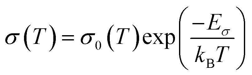 | (1) |
 | ||
| Fig. 4 Temperature-dependent in-plane conductivity of epi-BiVO4/YSZ. Conductivity, σ, plotted as ln(σT) vs. 103/T. The dashed line represents the fit to eqn (1), yielding a charge transport activation energy, Eσ, of 570 meV. In the inset, the conductivity is plotted against the temperature in a semi-log plot. | ||
The resulting charge transport activation barrier, Eσ, of 570 meV and the absolute conductivity (inset Fig. 4) are in excellent agreement with the previously reported values obtained from undoped BiVO4 on YSZ deposited via PLD.11 Interestingly, the films deposited by Zhang and co-workers were reported to comprise a single domain, whereas our films are characterized by twinning with domain boundaries. The finding of nearly identical transport barriers for both types of films suggests that in-plane transport is not significantly impacted by the presence of domain boundaries. This is surprising given that domain boundaries for epi-BiVO4 on indium-doped tin oxide (ITO) were found to act as high-conductivity channels for out-of-plane electrical transport,11 pointing to the need for improved understanding of planar defects in this material. Nevertheless, the electrical quality of the films is found to be commensurate with state-of-the-art material fabricated by PLD, thus confirming the applicability of solution-derived BiVO4 for fundamental studies of transport mechanisms.
Conclusions
We introduce a new solution-based synthesis method for wafer-scale epitaxial, monoclinic scheelite BiVO4 (010) on YSZ (001) substrates using spin-coating and metalorganic decomposition. The resulting films are compact, planar, and homogeneous with a high structural quality over a complete 2′′ wafer. Indeed, the small rocking curve FWHM of ∼0.04° indicates better structural order than analogous films deposited using much more advanced physical9–14 and chemical vapor deposition methods,16 and approaching those fabricated by MBE.15 This is an excellent result considering that our facile spin-coating process is performed in air at ambient pressure. Importantly, the continuous and compact nature of the films enables precise characterization of optoelectronic characteristics of BiVO4, which indicate small Urbach energies, low sub-band gap optical absorption, and thermally activated hopping transport comparable to films produced by PLD. Using these films, we experimentally characterize the large uniaxial optical anisotropy of BiVO4, confirming theoretical predictions and indicating a preferred orientation of BiVO4 (010) for capturing solar radiation. Thus, the facile spin-coating process for synthesis of epi-BiVO4 presented here can be accomplished without complex infrastructure, and enables high structural and optoelectronic quality material that is suitable for a broad range of fundamental studies necessary to advance understanding of the complex processes associated with light-to-chemical energy conversion.Conflicts of interest
There are no conflicts to declare.Acknowledgements
We acknowledge financial support from the Deutsche Forschungsgemeinschaft (DFG, German Research Foundation) under Germany's Excellence Strategy – EXC 2089/1 – 390776260 and TUM. Solar in the context of the Bavarian Collaborative Research Project Solar Technologies Go Hybrid (SolTech). J. E. acknowledges funding by the Deutsche Forschungsgemeinschaft (DFG, German Research Foundation) – 428591260 and support from the Bavarian Academy of Sciences and Humanities. A. H. acknowledges funding from the European Union's Horizon 2020 research and innovation programme under the Marie Skłodowska-Curie grant agreement No. 841556 and E. S. was supported by the European Research Council (ERC) under the European Union's Horizon 2020 research and innovation programme (grant agreement No. 864234). In addition, we thank Dr Thomas Wagner and Inga Potsch from J. A. Wollam for helpful discussion regarding VASE modelling. We thank Claudia Paulus for her contributions of establishing the underlying infrastructure for the chemical experiments, and Prof. Dr Hubert Gasteiger for the use of the Kratos Axis Ultra XPS system.Notes and references
- A. Kudo, K. Ueda, H. Kato and I. Mikami, Catal. Lett., 1998, 53, 229–230 CrossRef CAS.
- Y. Park, K. J. McDonald and K.-S. Choi, Chem. Soc. Rev., 2013, 42, 2321–2337 RSC.
- D. K. Lee, D. Lee, M. A. Lumley and K.-S. Choi, Chem. Soc. Rev., 2019, 48, 2126–2157 RSC.
- I. D. Sharp, J. K. Cooper, F. M. Toma and R. Buonsanti, ACS Energy Lett., 2017, 2, 139–150 CrossRef CAS.
- T. W. Kim and K.-S. Choi, Science, 2014, 343, 990–994 CrossRef CAS PubMed.
- J. K. Cooper, S. Gul, F. M. Toma, L. Chen, Y.-S. Liu, J. Guo, J. W. Ager, J. Yano and I. D. Sharp, J. Phys. Chem. C, 2015, 119, 2969–2974 CrossRef CAS.
- H. S. Han, S. Shin, D. H. Kim, I. J. Park, J. S. Kim, P.-S. Huang, J.-K. Lee, I. S. Cho and X. Zheng, Energy Environ. Sci., 2018, 11, 1299–1306 RSC.
- V. Nair, C. L. Perkins, Q. Lin and M. Law, Energy Environ. Sci., 2016, 9, 1412–1429 RSC.
- A. J. E. Rettie, S. Mozaffari, M. D. McDaniel, K. N. Pearson, J. G. Ekerdt, J. T. Markert and C. B. Mullins, J. Phys. Chem. C, 2014, 118, 26543–26550 CrossRef CAS.
- L. Meng, S. Kou, F. Zhang, C. Li and G. Li, J. Phys. D: Appl. Phys., 2020, 53, 225103 CrossRef CAS.
- W. Zhang, D. Yan, J. Li, Q. Wu, J. Cen, L. Zhang, A. Orlov, H. Xin, J. Tao and M. Liu, Chem. Mater., 2018, 30, 1677–1685 CrossRef CAS.
- G. Li, S. Kou, F. Zhang, W. Zhang and H. Guo, CrystEngComm, 2018, 20, 6950–6956 RSC.
- J. Song, M. J. Seo, T. H. Lee, Y.-R. Jo, J. Lee, T. L. Kim, S.-Y. Kim, S.-M. Kim, S. Y. Jeong, H. An, S. Kim, B. H. Lee, D. Lee, H. W. Jang, B.-J. Kim and S. Lee, ACS Catal., 2018, 8, 5952–5962 CrossRef CAS.
- C. N. Van, W. S. Chang, J.-W. Chen, K.-A. Tsai, W.-Y. Tzeng, Y.-C. Lin, H.-H. Kuo, H.-J. Liu, K.-D. Chang, W.-C. Chou, C.-L. Wu, Y.-C. Chen, C.-W. Luo, Y.-J. Hsu and Y.-H. Chu, Nano Energy, 2015, 15, 625–633 CrossRef CAS.
- S. Stoughton, M. Showak, Q. Mao, P. Koirala, D. A. Hillsberry, S. Sallis, L. F. Kourkoutis, K. Nguyen, L. F. J. Piper, D. A. Tenne, N. J. Podraza, D. A. Muller, C. Adamo and D. G. Schlom, APL Mater., 2013, 1, 042112 CrossRef.
- P. S. Archana, Z. Shan, S. Pan and A. Gupta, Int. J. Hydrogen Energy, 2017, 42, 8475–8485 CrossRef CAS.
- W. Zhang and M. Liu, ACS Energy Lett., 2019, 4, 834–843 CrossRef CAS.
- W. Wang, P. J. Strohbeen, D. Lee, C. Zhou, J. K. Kawasaki, K.-S. Choi, M. Liu and G. Galli, Chem. Mater., 2020, 32, 2899–2909 CrossRef CAS.
- D. Lee, W. Wang, C. Zhou, X. Tong, M. Liu, G. Galli and K.-S. Choi, Nat. Energy, 2021, 6, 287–294 CrossRef CAS.
- F. M. Toma, J. K. Cooper, V. Kunzelmann, M. T. McDowell, J. Yu, D. M. Larson, N. J. Borys, C. Abelyan, J. W. Beeman, K. M. Yu, J. Yang, L. Chen, M. R. Shaner, J. Spurgeon, F. A. Houle, K. A. Persson and I. D. Sharp, Nat. Commun., 2016, 7, 1–11 Search PubMed.
- J. Tauc, R. Grigorovici and A. Vancu, Phys. Status Solidi B, 1966, 15, 627–637 CrossRef CAS.
- H. R. Philipp, Handbook of Optical Constants of Solids, Elsevier, 1997, pp. 749–763 Search PubMed.
- T. Liu, X. Zhou, M. Dupuis and C. Li, Phys. Chem. Chem. Phys., 2015, 17, 23503–23510 RSC.
- A. W. Sleight, H.-y. Chen, A. Ferretti and D. E. Cox, Mater. Res. Bull., 1979, 14, 1571–1581 CrossRef CAS.
- M. Yashima, S. Sasaki, M. Kakihana, Y. Yamaguchi, H. Arashi and M. Yoshimura, Acta Crystallogr., Sect. B: Struct. Sci., 1994, 50, 663–672 CrossRef.
- K. Sayama, A. Nomura, T. Arai, T. Sugita, R. Abe, M. Yanagida, T. Oi, Y. Iwasaki, Y. Abe and H. Sugihara, J. Phys. Chem. B, 2006, 110, 11352–11360 CrossRef CAS PubMed.
- R. L. Frost, D. A. Henry, M. L. Weier and W. Martens, J. Raman Spectrosc., 2006, 37, 722–732 CrossRef CAS.
- M. Lamers, S. Fiechter, D. Friedrich, F. F. Abdi and R. van de Krol, J. Mater. Chem. A, 2018, 6, 18694–18700 RSC.
- J. Eichhorn, S. E. Reyes-Lillo, S. Roychoudhury, S. Sallis, J. Weis, D. M. Larson, J. K. Cooper, I. D. Sharp, D. Prendergast and F. M. Toma, Small, 2020, 16, 2001600 CrossRef CAS PubMed.
- J. D. Bierlein and A. W. Sleight, Solid State Commun., 1975, 16, 69–70 CrossRef CAS.
- C. Hill, M. C. Weber, J. Lehmann, T. Leinen, M. Fiebig, J. Kreisel and M. Guennou, APL Mater., 2020, 8, 081108 CrossRef CAS.
- C. Nguyen Van, T. H. Do, J.-W. Chen, W.-Y. Tzeng, K.-A. Tsai, H. Song, H.-J. Liu, Y.-C. Lin, Y.-C. Chen, C.-L. Wu, C.-W. Luo, W.-C. Chou, R. Huang, Y.-J. Hsu and Y.-H. Chu, NPG Asia Mater., 2017, 9, e357 CrossRef CAS.
- R. W. Schwartz, T. Schneller and R. Waser, C. R. Chim., 2004, 7, 433–461 CrossRef CAS.
- N. Bassiri-Gharb, Y. Bastani and A. Bernal, Chem. Soc. Rev., 2014, 43, 2125–2140 RSC.
- A. Queraltó, M. de la Mata, J. Arbiol, X. Obradors and T. Puig, Adv. Mater. Interfaces, 2016, 3, 1600392 CrossRef.
- S. Hao, M. Hetzl, V. F. Kunzelmann, S. Matich, Q. Sai, C. Xia, I. D. Sharp and M. Stutzmann, Appl. Phys. Lett., 2020, 116, 092102 CrossRef CAS.
- T. Das, X. Rocquefelte, R. Laskowski, L. Lajaunie, S. Jobic, P. Blaha and K. Schwarz, Chem. Mater., 2017, 29, 3380–3386 CrossRef CAS.
- Z. Zhao, Z. Li and Z. Zou, Phys. Chem. Chem. Phys., 2011, 13, 4746 RSC.
- K. Ding, B. Chen, Z. Fang and Y. Zhang, Theor. Chem. Acc., 2013, 132, 1352 Search PubMed.
- J. F. Li, A. S. Bhalla and L. E. Gross, Opt. Commun., 1992, 92, 115–118 CrossRef CAS.
- A. J. Rettie, W. D. Chemelewski, J. Lindemuth, J. S. McCloy, L. G. Marshall, J. Zhou, D. Emin and C. B. Mullins, Appl. Phys. Lett., 2015, 106, 022106 CrossRef.
- L. Friedman and T. Holstein, Ann. Phys., 1963, 21, 494–549 CAS.
Footnote |
| † Electronic supplementary information (ESI) available: Additional XRD, contact angle, Raman, XPS, AFM, pole figures, 2D reciprocal space maps, and ellipsometry data. See DOI: 10.1039/d1ta10732a |
| This journal is © The Royal Society of Chemistry 2022 |