
Preserving the stoichiometry of triple-cation perovskites by carrier-gas-free antisolvent spraying†
Oscar
Telschow
ab,
Miguel
Albaladejo-Siguan
 ab,
Lena
Merten
c,
Alexander D.
Taylor
ab,
Katelyn P.
Goetz
ab,
Tim
Schramm
ab,
Oleg V.
Konovalov
d,
Maciej
Jankowski
d,
Alexander
Hinderhofer
c,
Fabian
Paulus
b,
Frank
Schreiber
c and
Yana
Vaynzof
*ab
ab,
Lena
Merten
c,
Alexander D.
Taylor
ab,
Katelyn P.
Goetz
ab,
Tim
Schramm
ab,
Oleg V.
Konovalov
d,
Maciej
Jankowski
d,
Alexander
Hinderhofer
c,
Fabian
Paulus
b,
Frank
Schreiber
c and
Yana
Vaynzof
*ab
aIntegrated Center for Applied Physics and Photonic Materials, Technische Universität Dresden, Nöthnitzer Straße 61, 01187 Dresden, Germany. E-mail: yana.vaynzof@tu-dresden.de; Web: https://cfaed.tu-dresden.de/cfeet-about Web: http://www.twitter.com/vaynzof
bCenter for Advancing Electronics Dresden (cfaed), Technische Universität Dresden, Helmholtzstraße 18, 01069 Dresden, Germany
cInstitut für Angewandte Physik, Universität Tübingen, 72076 Tübingen, Germany
dThe European Synchrotron-ESRF, 71 Avenue des Martyrs, CS 40220, 38043 Grenoble Cedex 9, France
First published on 11th February 2022
Abstract
The use of antisolvents during the fabrication of solution-processed lead halide perovskite layers is increasingly common. Usually, the antisolvent is applied by pipetting during the spin-coating process, which often irreversibly alters the composition of the perovskite layer, resulting in the formation of PbI2 at the surface and bulk of the perovskite layer. Here, we demonstrate that by applying the antisolvent via carrier-gas free spraying, the stoichiometry of the perovskite layer is far better preserved. Consequently, the photovoltaic performance of triple cation photovoltaic devices fabricated in an inverted architecture is enhanced, mainly due to an increase in the open-circuit voltage. By exploring different volumes of antisolvent, we show that spraying as little as 60 μL results in devices with power conversion efficiencies as high as 21%. Moreover, solar cells with sprayed antisolvent are more stable than those fabricated by pipetting the antisolvent.
 Yana Vaynzof | Prof. Dr Yana Vaynzof is the Chair for Emerging Electronic Technologies at the Integrated Center for Applied Physics and Photonic Materials and the Center for Advancing Electronics Dresden at the Technical University of Dresden (Germany). She received a BSc in Electrical Engineering from the Technion – Israel Institute of Technology (Israel) in 2006 and a MSc In Electrical Engineering from Princeton University (USA) in 2008. In 2011, she received a PhD in Physics from the University of Cambridge (UK). Her research interests lie in the field of emerging photovoltaics focusing on the study of material and device physics of organic, quantum dot and perovskite solar cells by integrating device fabrication and characterisation with the application and development of advanced spectroscopic methods. |
Introduction
The remarkable progress in the development of photovoltaic devices based on lead halide perovskites makes them particularly promising for industrial integration.1–4 However, the most efficient devices are still fabricated using the so-called ‘solvent-engineering’ method,5,6 in which an antisolvent is used to trigger the crystallization of the perovskite layer during the spin-coating of the perovskite precursor solution (Fig. 1a). This has led to extensive optimization of the antisolvent application step, including, among others, parameters such as choice of solvent,7 its volume,8,9 temperature10,11 and application timing,12 which has led to the demonstration of high-efficiency photovoltaic devices. Despite this optimization, there are several drawbacks of the current method of antisolvent application. First of all, depositing the antisolvent by pipetting it onto the wet perovskite films commonly results in the use of relatively large volumes of antisolvent (hundreds of μL) to ensure the coating of the surface of the entire sample.13,14 Consequently, the large volume of available antisolvent often leads to interactions with the underlying wet perovskite layer that can irreversibly modify its stoichiometry. For example, even a minute solubility of the perovskite precursors (e.g. organic halides) in the antisolvent may lead to their diffusion across the liquid–liquid interface (between the wet perovskite film and the antisolvent) and their removal from the perovskite layer.15,16 This might explain why perovskite films made from a perfectly stoichiometric solution result in a non-stoichiometric composition, with excess PbI2 observed in either scanning-electron microscopy (SEM) or X-ray diffraction (XRD) measurements.15,17,18 Furthermore, the use of large volumes of antisolvent raises concerns about the scalability of deposition via the solvent engineering method,19,20 as well as the environmental impact of these solvents.21,22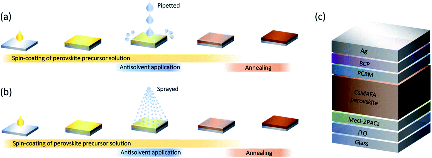 | ||
| Fig. 1 Schematic depiction of the perovskite layer fabrication process via (a) pipetted and (b) sprayed antisolvent application. (c) Schematic structure of the photovoltaic devices fabricated in this work. | ||
These drawbacks motivate the search for alternative methods for the application of antisolvents. Spraying was investigated as an alternative method for dispensing the antisolvent by several researchers aiming in particular to improve the homogeneity of perovskite samples. Early work by Ye et al. showed that spraying the antisolvent using dry air as a carrier gas led to the formation of smoother, more uniform films, while dispensing the antisolvent by pipetting resulted in coffee-ring effects.23 While the authors did not specify the volume of the sprayed/pipetted antisolvent, they reported that the optimal devices were obtained by continuously spraying the wet perovskite film for 19–24 s using a high carrier-gas flow of 90 L h−1. These parameters suggest that the volume of sprayed antisolvent was relatively high. Similarly, improved surface coverage and homogeneity were observed when spraying large area perovskite films using a carrier-gas (unspecified) assisted spraying at 60 psi for 3 s.24 A more recent study by Lee et al. has explored spraying mixed antisolvents (acetonitrile/chlorobenzene at various ratios) as a method to suppress the inhomogeneities the authors observed when dispensing the mixed antisolvents by pipetting.25 Despite these promising results, carrier-gas-assisted spraying has several limitations. The use of a carrier-gas might introduce additional artifacts, as the flow of gas onto the wet perovskite film might impact the drying dynamics. Furthermore, past results have shown that carrier-gas assisted spraying requires longer application times (varying from 3 to 24 s of continuous spraying), which adds to the antisolvent consumption and might irreversibly affect the composition of the perovskite layer.
In this work, we explore carrier-gas-free spraying as a method for antisolvent application (Fig. 1b). In this simple method, the antisolvent is introduced into a vessel with a thin tube connected to a pump. Upon pressing on the pump trigger, the antisolvent is forced through a one-way valve into a nozzle, creating a mist of antisolvent droplets that land on the wet perovskite film. This method allows dispensing of the antisolvent very quickly and in fixed quantities, unlike the continuous spraying that occurs in the carrier-gas-assisted method. The overall amount of antisolvent interacting with the wet perovskite film can be tuned by controlling the number of spray cycles and the height from which the antisolvent is sprayed. The spraying bottle and bottle holder we used can be seen in Fig. S1.† We focus on the fabrication of stoichiometric triple-cation mixed-halide perovskite (Cs0.05(MA0.17FA0.83)0.95Pb(I0.9Br0.1)3) films and compare the deposition of different volumes of antisolvent (60 μL and 200 μL) by either pipetting or carrier-gas-free spraying. We find that solar cells fabricated when spraying the antisolvent outperform those in which the antisolvent was pipetted, reaching a maximum power conversion efficiency (PCE) of 21%. Scanning electron microscopy (SEM) and grazing incidence wide angle X-ray scattering (GIWAXS) studies reveal that the sprayed samples exhibit a strongly reduced PbI2 content as compared to the pipetted ones, suggesting a much better preservation of the intended stoichiometry of the perovskite films. This leads to an improvement in the open-circuit voltage (VOC) of the devices and an improved shelf-stability.
Experimental
A detailed description of device fabrication and experiments can be found in the ESI.† Experimental X-ray scattering data can be found at: DOI: http://10.15151/ESRF-ES-406842143.Results and discussion
Photovoltaic device performance
To investigate the efficacy of carrier-gas-free antisolvent spraying in the formation of high-quality perovskite layers, we fabricated solar cells in an inverted architecture, the structure of which is shown in Fig. 1c. The photovoltaic parameters of the best 24 solar cells of each kind are presented in Fig. 2. For both volumes of antisolvent (60 or 200 μL of trifluorotoluene, TFT) the VOC of the sprayed devices is on average 20–30 mV higher than for the pipetted ones. The short-circuit current (JSC) of the sprayed devices also shows a minor increase, especially evident for the low volume of antisolvent. The fill factors (FF) remain essentially unchanged, with most devices resulting in FF > 80%. These improvements lead to a higher PCE of the sprayed devices, with an average PCE > 20% and a maximum PCE of 21%. The current–voltage (J–V) characteristics of the best-performing devices of each kind are shown in Fig. S2† and their photovoltaic performance parameters are summarized in Table S1.† While both pipetted and sprayed devices exhibit negligible hysteresis, it is noteworthy that the hysteresis of the sprayed devices is particularly low.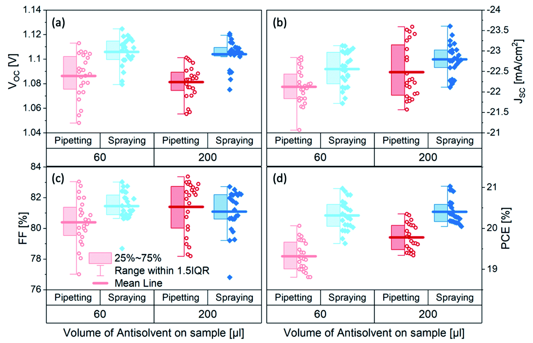 | ||
| Fig. 2 (a) VOC (b) JSC (c) FF and (d) PCE of triple cation perovskite solar cells fabricated by either spraying (blue diamonds) or pipetting (red circles) 60 or 200 μL of TFT as antisolvent. | ||
Interestingly, increasing the antisolvent volume led to an increase in the performance of the pipetted devices – in agreement with earlier observations15 – but the performance of the sprayed devices was similarly good for both 60 μL and 200 μL of antisolvent. We also tested devices fabricated using 90 μL of antisolvent and found that the average device performance of sprayed devices was similar to that of devices fabricated using 60 μL and 200 μL of antisolvent, suggesting the performance of sprayed devices are not impacted by the volume of sprayed antisolvent (Fig. S3†). Pipetted devices with 90 μL showed a similar average performance to that of 200 μL devices. We emphasize that the architecture of the devices, the extraction layers and all other fabrication parameters were kept the same, so the improvement in the photovoltaic performance is associated solely with the method of antisolvent application.
Since the performance improvement originates mainly from the changes in VOC, we explored whether this variance arises from a different bandgap of the perovskite layers. UV-vis measurements (Fig. 3a) confirmed that regardless of the antisolvent application method, the bandgap of the sprayed/pipetted perovskite layers remains unchanged. Another possibility for the increase in VOC is that the non-radiative losses are suppressed for devices with sprayed antisolvent.26 To explore that, we measured the photoluminescence (PL) of complete photovoltaic devices of each kind (Fig. 3b). We find that the PL of sprayed devices is significantly higher than that of the pipetted ones. Consequently, their PL quantum efficiency (PLQE) is more than doubled as compared to the pipetted solar cells (see inset). The enhanced PLQE is consistent with the observed increase in VOC, suggesting that perovskite films fabricated with sprayed antisolvent exhibit a lower density of non-radiative recombination centers.
 | ||
| Fig. 3 (a) Absorption spectra of triple cation perovskite thin films and (b) photoluminescence spectra and photoluminescence quantum efficiency (PLQE) of triple cation perovskite solar cells fabricated by either spraying or pipetting either 60/200 μL of TFT. | ||
Structural characterization of pipetted and sprayed perovskite films
To investigate the microstructure of perovskite films fabricated by either pipetting or spraying the antisolvent, the films were characterized by SEM. All films show the typical compact polycrystalline microstructure with grains ranging from 100 nm to 400 nm in size. In the case of films fabricated by pipetting the antisolvent (Fig. 4a and b), we also observe multiple crystallites at the surface of the perovskite film (marked in red) that are commonly associated with the presence of phase-separated PbI2 in the perovskite film.27,28 On the other hand, samples fabricated by spraying the antisolvent (Fig. 4c and d) show significantly fewer of such PbI2 crystallites.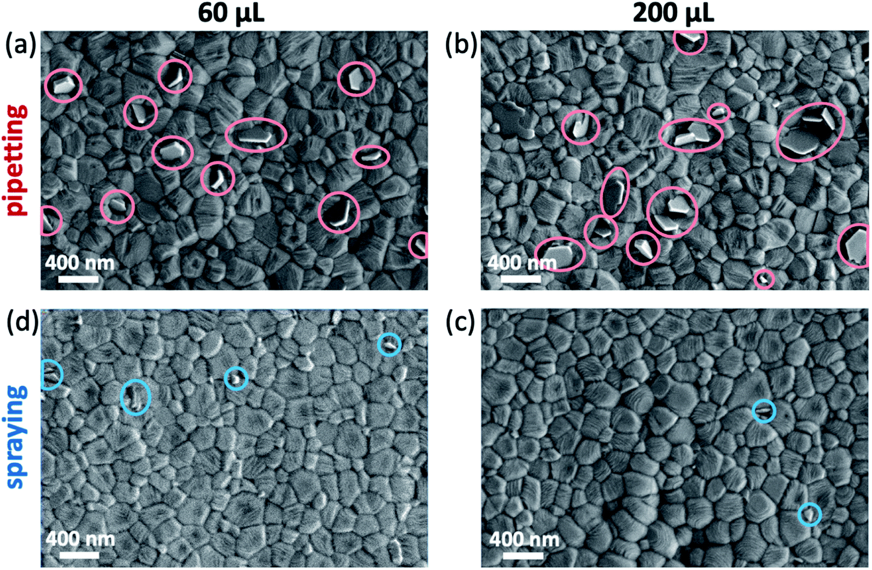 | ||
| Fig. 4 Scanning electron microscopy (SEM) images of triple cation perovskite thin films fabricated by either (a and b) pipetting or (c and d) spraying 60/200 μL of TFT. | ||
To further investigate the crystalline structure of the perovskite films, they were characterized by GIWAXS (Fig. 5a–d). The experimental configuration of the GIWAXS measurements was similar to that in earlier works.29–31 In all cases, the samples exhibit the typical triple cation crystal structure (ESI, Fig. S4†) with a small contribution of excess PbI2 phase. Quantitatively, the PbI2 volume fraction in all samples is larger at the surface compared to the bulk of the films. Furthermore, samples formed by pipetting the antisolvent exhibit a higher PbI2 content than sprayed samples at both the surface and the bulk of the perovskite layers (Fig. 5e).
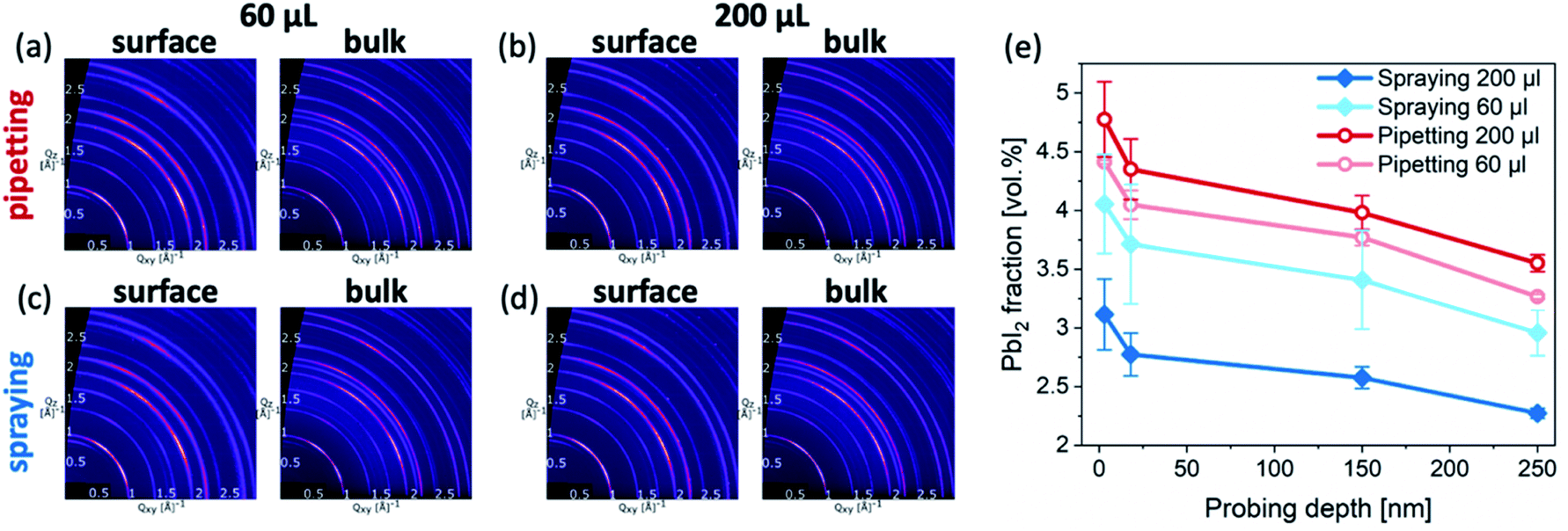 | ||
| Fig. 5 Reciprocal space maps (obtained by GIWAXS measurements) of triple cation perovskite thin films fabricated by either (a and b) pipetting or (c and d) spraying 60/200 μL of TFT (e) volume fraction of PbI2 at different depths of the different perovskite films. | ||
Taken together with the SEM images, these results suggest that spraying the antisolvent far better preserves the intended stoichiometry of the perovskite layers. We note that unlike many reports, in which excess PbI2 is intentionally introduced into the perovskite composition,32,33 the intended composition of the perovskite films in our study is perfectly stoichiometric. Consequently, the presence of PbI2 domains suggests that a certain fraction of organic halides was absent during the crystallization of the perovskite layer. Such a loss of organic halides is likely to occur during the application of an antisolvent, even for antisolvents that do not easily dissolve organic halides, such as TFT.
Considering the differences between the two antisolvent application methods offers an explanation for the variation in the final composition of the perovskite layers. When dispensing the antisolvent by pipetting, its large volume comes in contact with the wet perovskite film, allowing the diffusion of organic halides such as methylammonium iodide (MAI) and formamidinium iodide (FAI) from the wet perovskite film into the antisolvent, which due to the high centrifugal forces is spun off the surface of the sample (Fig. 6). With a certain fraction of organic halides lost, the remaining precursors crystallize into a perovskite film that contains a certain amount of PbI2. The impact is strongest at the surface of the perovskite film, but is evident also in its bulk. On the other hand, by spraying the antisolvent, it interacts with the surface of the sample as a mist of small droplets. The relatively small volume of each droplet significantly lowers the maximum possible amount of organic halides that can diffuse into the antisolvent. Moreover, the large surface area of the sprayed droplets results in an accelerated evaporation, which is significantly more rapid than that of the pipetted antisolvent volume. Finally, the droplets are less likely to be spun off the surface of the sample due to their lower mass. All these factors contribute to the far better preservation of the intended perovskite composition in the final crystallized film.
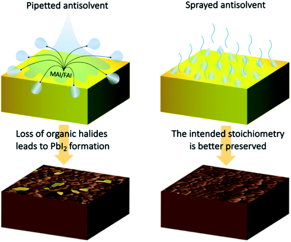 | ||
| Fig. 6 Schematic presentation of the differences between pipetting and spraying the antisolvent and the resultant film stoichiometry. | ||
The presence of larger amounts of PbI2 in the pipetted perovskite films results not only in a reduced initial photovoltaic performance, but also in a reduced device stability. We tracked the performance of unencapsulated solar cells fabricated with either spraying or pipetting the antisolvent over a period of two months (Fig. S5†). Between measurements, the devices were kept in darkness and ambient air. While both types of devices show a significant decrease in performance, we find that the sprayed devices are generally more stable than the pipetted ones. This is consistent with previous reports, showing that unreacted PbI2 can have detrimental effects on the stability of perovskite solar cells,34 and that its removal by various surface modification methods can lead to improved performance and stability.35
Conclusions
Our results indicate that the formation of unreacted PbI2 can be largely avoided by application of the antisolvent by carrier-gas free spraying rather than pipetting. This enables the fabrication of high efficiency devices using a relatively low volume of antisolvent (60 μL). Considering the simplicity of the spraying method, which requires no additional setups or equipment, we believe this method can be widely adopted by other researchers. Moreover, these results also open the route for fabricating more efficient and stable devices in large-area production where spraying is particularly suitable.Author contributions
O. T. fabricated the perovskite layers and devices and performed the optical, PL and PV characterisation experiments. A. D. T. and T. S. assisted with device fabrication and characterisation M. A.-S. and K. P. G. performed the SEM measurements. L. M., O. V. K., M. J. and A. H. performed the GIWAXS measurements and analysis under the supervision of F. S. F. P. assisted with the analysis of the results and the development of the proposed mechanism. Y. V. supervised the project and wrote the manuscript which was edited by all co-authors.Conflicts of interest
There are no conflicts to declare.Acknowledgements
This work is financially supported by the European Research Council (ERC) under the European Union's Horizon 2020 research and innovation program (ERC Grant Agreement No. 714067, ENERGYMAPS). We acknowledge the Deutsche Forschungsgemeinschaft (DFG) for funding the “PROCES” project (Grant No. VA 991/2-1) and the “PERFECT PVs” project (Grant No. 424216076) and the “PHIVE-X” project (SCHR 700/38-1) in the framework of SPP 2196. We also thank the BMBF for funding (project 05K19VTA). Finally, we kindly acknowledge the European Synchrotron Radiation Facility for provision of synchrotron radiation facilities and the Dresden Center for Nanoanalysis in the cfaed for providing access to the electron microscopy facilities.Notes and references
- J. Y. Kim, J.-W. Lee, H. S. Jung and N.-G. Park, Chem. Rev., 2020, 120(15), 7867–7918 CrossRef CAS PubMed.
- L. Schmidt-Mende, V. Dyakonov, S. Olthof, F. Ünlü, K. M. T. Lê, S. Mathur, A. D. Karabanov, D. C. Lupascu, L. M. Herz and A. Hinderhofer, et al. , APL Mater., 2021, 9(10), 109202 CrossRef CAS.
- Y. Zhou and M. Saliba, ACS Energy Lett., 2021, 6(8), 2750–2754 CrossRef CAS.
- Y. Cheng and L. Ding, Energy Environ. Sci., 2021, 14, 3233–3255 RSC.
- N. J. Jeon, J. H. Noh, Y. C. Kim, W. S. Yang, R. Seungchan and S. I. Seok, Nat. Mater., 2014, 13, 897–903 CrossRef CAS PubMed.
- S. Ghosh, S. Mishra and T. Singh, Adv. Mater. Interfaces, 2020, 7(18), 2000950 CrossRef CAS.
- M. Xiao, L. Zhao, M. Geng, Y. Li, B. Dong, Z. Xu, L. Wan, W. Li and S. Wang, Nanoscale, 2018, 10, 12141–12148 RSC.
- K. M. Lee, C. J. Lin, B. Y. Liou, S. M. Yu, C. C. Hsu, V. Suryanarayanan and M. C. Wu, Sol. Energy Mater. Sol. Cells, 2017, 172, 368 CrossRef CAS.
- M. Wang, Q. Fu, L. Yan, P. Guo, L. Zhou, G. Wang, Z. Zheng and W. Luo, ACS Appl. Mater. Interfaces, 2019, 11(4), 3909–3916 CrossRef CAS PubMed.
- Y.-K. Ren, X.-H. Ding, Y.-H. Wu, J. Zhu, T. Hayat, A. Alsaedi, Y.-F. Xu, Z.-Q. Li, S.-F. Yang and S.-Y. Dai, J. Mater. Chem. A, 2017, 5, 20327–20333 RSC.
- H. Taherianfard, G. W. Kim, M. M. Byranvand, K. Choi, G. Kang, H. Choi, F. Tajabadi, N. Taghavinia and T. Park, ACS Appl. Energy Mater., 2020, 3, 1506 CrossRef CAS.
- J. Kumar, R. Kumar, K. Frohna, D. Moghe, S. D. Stranks and M. Bag, Phys. Chem. Chem. Phys., 2020, 22, 26592 RSC.
- J. Yi, J. Zhuang, Z. Ma, Z. Guo, W. Zhou, S. Zhao, H. Zhang, X. Luo and H. Li, Org. Electron., 2019, 69, 69 CrossRef CAS.
- S. Paek, P. Schouwink, E. N. Athanasopoulou, K. T. Cho, G. Grancini, Y. Lee, Y. Zhang, F. Stellacci, M. K. Nazeeruddin and P. Gao, Chem. Mater., 2017, 29, 3490 CrossRef CAS.
- A. D. Taylor, Q. Sun, K. P. Goetz, Q. An, T. Schramm, Y. Hofstetter, M. Litterst, F. Paulus and Y. Vaynzof, Nat. Commun., 2021, 12, 1878 CrossRef CAS PubMed.
- Q. An, L. Vieler, K. P. Goetz, O. Telschow, Y. J. Hofstetter, R. Buschbeck, A. D. Taylor and Y. Vaynzof, Advanced Energy and Sustainability Research, 2021, 2(11), 2100061 CrossRef.
- A. S. Yeramilli, Y. Chen and T. L. Alford, Sustain. Energy Fuels, 2021, 5, 2486–2493 RSC.
- Y. Hu, M. F. Ayguler, M. L. Petrus, T. Bein and P. Docampo, ACS Energy Lett., 2017, 2(10), 2212–2218 CrossRef CAS.
- Y. Vaynzof, Adv. Energy Mater., 2020, 10(48), 2003073 CrossRef CAS.
- R. Swartwout, M. T. Hoerantner and V. Bulović, Energy Environ. Mater., 2019, 2, 119 CrossRef CAS.
- M. Zhang, D. Xin, X. Zheng, Q. Chen and W.-H. Zhang, ACS Sustainable Chem. Eng., 2020, 8(35), 13126–13138 CrossRef CAS.
- K. P. Goetz, A. D. Taylor, Y. J. Hofstetter and Y. Vaynzof, ACS Appl. Mater. Interfaces, 2021, 13(1), 1–17 CrossRef CAS PubMed.
- J. Ye, X. Zhang, L. Zhu, H. Zheng, G. Liu, H. Wang, T. Hayat, X. Pan and S. Dai, Sustain. Energy Fuels, 2017, 1, 907–914 RSC.
- J. Kim, J. S. Yun, Y. Cho, D. S. Lee, B. Wilkinson, A. M. Soufiani, X. Deng, J. Zheng, A. Shi, S. Lim, S. Chen, Z. Hameiri, M. Zhang, C. F. J. Lau, S. Huang, M. A. Green and A. W. Y. Ho-Baillie, ACS Energy Lett., 2017, 2(9), 1978–1984 CrossRef CAS.
- D. S. Lee, J. Bing, J. Kim, M. A. Green, S. Huang and A. W. Y. Ho-Baillie, Sol. RRL, 2020, 4(1), 1900397 CrossRef CAS.
- K. P. Goetz, A. D. Taylor, F. Paulus and Y. Vaynzof, Adv. Funct. Mater., 2020, 30(23), 1910004 CrossRef CAS.
- D. Shan, G. Tong, Y. Cao, M. Tang, J. Xu, L. Yu and K. Chen, Nanoscale Res. Lett., 2019, 14, 208 CrossRef PubMed.
- B. Roose, K. Dey, Y.-H. Chiang, R. H. Friend and S. D. Stranks, J. Phys. Chem. Lett., 2020, 11(16), 6505–6512 CrossRef CAS PubMed.
- A. Greco, A. Hinderhofer, M. Dar, A. Ibrahim, N. Arora, J. Hagenlocher, A. Chumakov, M. Grätzel and F. Schreiber, J. Phys. Chem. Lett., 2018, 9, 6750 CrossRef CAS PubMed.
- L. Merten, A. Hinderhofer, T. Baumeler, N. Arora, J. Hagenlocher, S. Zakeeruddin, M. Dar, M. Grätzel and F. Schreiber, Chem. Mater., 2021, 33, 2769 CrossRef CAS.
- M. I. Dar, A. Hinderhofer, G. Jacopin, V. Belova, N. Arora, S. M. Zakeeruddin, F. Schreiber and M. Grätzel, Adv. Funct. Mater., 2017, 27, 1701433 CrossRef.
- M. Saliba, T. Matsui, J.-Y. Seo, K. Domanski, J.-P. Correa-Baena, M. K. Nazeeruddin, S. M. Zakeeruddin, W. Tress, A. Abate, A. Hagfeldt and M. Grätzel, Energy Environ. Sci., 2016, 9, 1989–1997 RSC.
- B.-W. Park, N. Kedem, M. Kulbak, D. Y. Lee, W. S. Yang, N. J. Jeon, J. Seo, G. Kim, K. J. Kim, T. J. Shin, G. Hodes, D. Cahen and S. Il Seok, Nat. Commun., 2018, 9, 3301 CrossRef PubMed.
- G. Tumen-Ulzii, C. Qin, D. Klotz, M. R. Leyden, P. Wang, M. Auffray, T. Fujihara, T. Matsushima, J.-W. Lee, S.-J. Lee, Y. Yang and C. Adachi, Adv. Mater., 2020, 32(16), 1905035 CrossRef CAS PubMed.
- Z. Hu, Q. An, H. Xiang, L. Aigouy, B. Sun, Y. Vaynzof and Z. Chen, ACS Appl. Mater. Interfaces, 2020, 12(49), 54824–54832 CrossRef CAS PubMed.
Footnote |
| † Electronic supplementary information (ESI) available. See DOI: 10.1039/d1ta10566c |
| This journal is © The Royal Society of Chemistry 2022 |