
Influence of intrinsic defects on the structure and dynamics of the mixed Pb–Sn perovskite: first-principles DFT and NAMD simulations†
Qi
Liu
ab,
Akang
Li
ab,
Weibin
Chu
 cd,
Oleg V.
Prezhdo
*cd and
WanZhen
Liang
*ab
cd,
Oleg V.
Prezhdo
*cd and
WanZhen
Liang
*ab
aState Key Laboratory of Physical Chemistry of Solid Surfaces, Collaborative Innovation Center of Chemistry for Energy Materials, Fujian Provincial Key Laboratory of Theoretical and Computational Chemistry, People's Republic of China. E-mail: liangwz@xmu.edu.cn
bDepartment of Chemistry, College of Chemistry and Chemical Engineering, Xiamen University, Xiamen, Fujian 361005, People's Republic of China
cDepartment of Chemistry, University of Southern California, Los Angeles, California 90089, USA. E-mail: prezhdo@usc.edu
dDepartment of Physics and Astronomy, University of Southern California, Los Angeles, California 90089, USA
First published on 24th November 2021
Abstract
The mixed tin (Sn) and lead (Pb) perovskite compositions have shown great potential in perovskite photovoltaic devices due to the significantly enhanced material stability and prolonged carrier lifetime, compared to the pure Sn halide perovskites. In spite of the increasing interest, the behaviors of photo-generated charges and of the intrinsic point defects, such as the metal cation vacancies (VSn and VPb) and the interstitial halogen (iI), have not been well understood in this class of materials. We report first-principles density functional theory (DFT) calculations combined with ab initio non-adiabatic molecular dynamics (NAMD) simulations on the static and dynamic structures of MA2SnPbI6 with and without these intrinsic defects. We discuss the nature of the defect states and unveil the influence of the intrinsic point defects on the structure, optoelectronic properties, and charge carrier dynamics of MA2SnPbI6. The iI defect significantly shortens the carrier lifetime by creating mid-gap states that provide new recombination pathways. In comparison, the vacancy defects have much weaker influence on the carrier lifetime. Both VSn and VPb produce the defect states just below the valence band maxima (VBMs), and do not alter the band gap. They affect the carrier lifetime through changing the energy dispersions of VBMs and the conduction band minima (CBMs). We suggest that excess cations should be used in the synthesis of perovskites to avoid the appearance of interstitial halogen defects.
1 Introduction
Perovskite solar cells (PSCs) have been intensively studied in the past decade because of their high power-conversion-efficiency (PCE), low cost and easy synthesis.1–7 The first PSC was designed by Miyasaka et al. with a PCE of only 3.8%.3 Subject to the rapid advances over the past ten years, the certified PCE increased quickly to 29.5%.8 These developments have demonstrated the great potential of PSCs as the next-generation low-cost solar technology. Unfortunately, the most efficient PSCs all contain Pb. The Pb-induced pollution and poisoning are serious environmental concerns, which have hampered the commercialization of the technologies based on these materials. Developing alternative strategies to minimize the impact of toxic Pb on the environment under the premise of maintaining the photoelectric activity of perovskite materials has become an important topic in perovskite photovoltaics.2,7,9–11To reduce or eliminate the content of Pb, scientists have suggested to develop PSCs containing less Pb and Pb-free PSCs.12–16 One idea is to develop Pb-free PSCs by replacing Pb with other elements. The earliest suggestion was to replace Pb with Sn and Ge, group 14 elements with comparable ionic radii.17,18 Later, transition metals such as Cu, Mn, Fe, Co, and Ni were identified as promising alternatives to Pb, owing to their rich chemistries and multiple oxidation states. However, these Pb-free compounds suffer from poor efficiency and stability.
Another idea is to replace two divalent Pb(II) ions with monovalent and trivalent ions. Experimentalists have successfully synthesised double perovskites by using heterovalent substitution with monovalent Cu, Ag, Au or even alkali-metals, and trivalent In, Sb, and Bi cations.19–32 However, these kinds of Pb-free perovskite materials possess serious flaws in optoelectronic properties, which make them less likely candidates for PSCs. For example, the most easily synthesized Ag–Bi and Ag–Sb double perovskites19,20,23,33 have an indirect band gap, which will lead to a large amount of solar energy dissipated into heat after the carrier excitation.34
The PCE of Ag–Bi double perovskite-based PSCs is much lower than that of Pb-based, and even Sn-based PSCs. It is about 1.25% in its maximum.33 In addition, because AgI is highly sensitive to light, this kind of material cannot be filled with iodide cations, resulting in a wide band gap. The bulk phase of the In(I)–Bi(III) based perovskite has been predicted theoretically.35 It has a direct band gap and a carrier effective mass similar to that of the traditional Pb-bearing materials. However, the stability of monovalent In+ is lower than that of Ag+ and Tl+, and it has been reported experimentally that Cs2In(I)In(III)X6 perovskites are stable only at high temperature, while low temperature can cause a rotation between In(I) octahedra and In(III) octahedra, which leads to further degradation.36
An increasing number of studies have shown that it is difficult to eliminate Pb from high-performance PSCs. The more stable and better performing photoelectric materials are those still containing Pb, but in reduced amounts.18,37–46 In such compounds, Pb is partially replaced by other elements, including Sn, Ge, Sr, or other alkaline-earth-metals. At present, the practical scheme is to adopt a mixed Sn–Pb composition, and to decrease the Pb content as much as possible, in order to reduce the environmental toxicity of Pb while maintaining the working stability of the device. For instance, Ramirez et al. adopted a 1![[thin space (1/6-em)]](https://www.rsc.org/images/entities/char_2009.gif) :1.5 stoichiometric Sn:Pb ratio and reported a relatively high PCE of 10.5%.47 Kapil et al. produced a spike structure of the Pb–Sn mixed perovskite and reached a 17.6% PCE.48 Lanzetta et al. explained the surface-oxidation mechanism of Pb–Sn based perovskites.49 Long et al.50 discovered that the presence of Sn enhances the carrier lifetime of the traditional Pb-bearing perovskites.
:1.5 stoichiometric Sn:Pb ratio and reported a relatively high PCE of 10.5%.47 Kapil et al. produced a spike structure of the Pb–Sn mixed perovskite and reached a 17.6% PCE.48 Lanzetta et al. explained the surface-oxidation mechanism of Pb–Sn based perovskites.49 Long et al.50 discovered that the presence of Sn enhances the carrier lifetime of the traditional Pb-bearing perovskites.
When Sn(II) is exposed to air, it oxidizes spontaneously to form Sn(IV). Such a process leads to formation of various intrinsic defects,42,51,52 which have a severe impact on the optoelectronic properties of the material.53–63 The most common intrinsic defects generated in Pb–Sn perovskites include the Pb and Sn vacancies (VPb and VSn), and the interstitial iodide (iI), which can be formed by the following chemical processes.
| MASn(II)I3 + MAPbI3 − 2e− − Pb2+ = MASn(IV)I32+ + MA[VPb]I32−; |
| MASn(II)I3 + MASn(II)I3 − 2e− − Sn2+ = MASn(IV)I32+ + MA[VSn]I32−; |
| MASn(II)I3 + I− − 2e− = MASn(IV)I32+ + iI−. |
In this work, we study the structure, and the static and dynamic properties of the mixed Pb–Sn perovskite, and elucidate how the structure, and the optoelectronic and photoelectric properties are influenced by the intrinsic defects that are formed by the oxidation of Sn(II). We perform both first-principles density functional theory (DFT) calculations and non-adiabatic molecular dynamics (NAMD) simulations to obtain the fundamental insights, guiding the construction of high performance PSCs. We generate a microscopic understanding of the characteristics of the materials with and without the intrinsic defects, and study the nature of the defect states, which usually play a decisive role in determining carrier recombination and diffusion lengths in solar cells, and explain why the photophysical properties of mixed Sn–Pb perovskites are enhanced considerably compared to those of Sn-based crystals.
2 Computational details
The first-principles DFT simulations were performed with the Vienna Ab Initio Simulation Package (VASP)64–66 to study the geometric and electronic structures of the pristine and defective MA2SnPbI6 perovskite series. Unless otherwise specified, the generalized gradient approximation exchange-correlation functional of Perdew–Burke–Ernzerhof (PBE)66 was adopted in the calculations. Since PBE tends to underestimate bandgaps, we employed the HSE06 functional67,68 for benchmark calculations. HSE06 includes a fraction of screened Hartree–Fock exchange, α = 0.25, improving the discontinuity in the Kohn–Sham potential derivative for integer numbers of electrons.The spin–orbit coupling (SOC) effect is taken into account in the electronic structure calculations.
The electronic constituents are 4d 5s 5p for Sn, 5d 6s 6p for Pb, 5p 6s for I, 2s 2p for C and N, and 1s for H. For all the bulk-like systems, we adopted the Γ-point only for the HSE06 + SOC calculations, 4 × 4 × 4 Γ-centered k-point grid generated by the Monkhorst–Pack scheme for detailed properties obtained with PBE + SOC, and 12 × 12 × 12 linear scheme for the band-structure calculation with PBE + SOC. The projector augmented wave pseudopotentials with the cutoff energy of 500 eV were employed.
Considering the interaction between the hydrogen atoms and high-electronegativity groups, the PBE with the DFT-D3 dispersion correction of Grimme with zero-damping69–71 was applied to optimize the geometric structures. During the optimization of the geometries, all structures were allowed to relax to ensure that each atom was in mechanical equilibrium without any residual force larger than 10−4 eV Å−1.
Once the geometry optimization was completed, the repeated velocity rescaling was performed to equilibrate the structures at 300 K for 5 ps. Then, 8 ps adiabatic molecular dynamics trajectories were obtained within the microcanonical ensemble with the molecular dynamics time step set to 1 fs. To perform the NAMD simulations, we computed the non-adiabatic couplings dij using the time-domain numerical method72via the overlap between orbitals i and j at sequential time steps 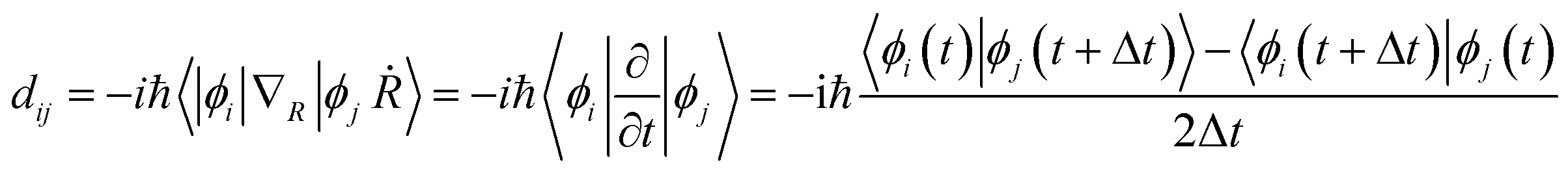 .
.
The non-adiabatic coupling is proportional to the overlap of the wavefunctions between the initial (i) and final (j) states, −iℏ〈ϕi|∇R|ϕj〉, and the nuclear velocity, dR/dt. The final 6000 configurations of the microcanonical molecular dynamics trajectories were selected as initial geometries for the following NAMD simulations of the nonradiative charge relaxation and electron–hole recombination with the Python extension for Ab Initio Dynamics code.73,74 Since the structures had direct bandgaps located at the Γ-point, the NA couplings were computed for the Γ-point only.
3 Results and discussion
3.1 Geometric structures
At first, we optimize all the possible structures of pristine MA2SnPbI6 to determine which kind of topological arrangement of the metal cations gives the highest stability. For this reason, we build a few cubic perovskite-phase MA2SnPbI6 structures with different arrangements of Pb and Sn atoms, as shown in Fig. 1. Then, we optimize them and calculate their free energies. The results in Table 1 prove that the structure in Fig. 1(c) with the face-to-face arrangement of Pb and Sn atoms possesses the best thermal stability. This minimum unit cell is able to generate all internal point defects. Thus, this configuration is adopted in the later study at an affordable computational cost.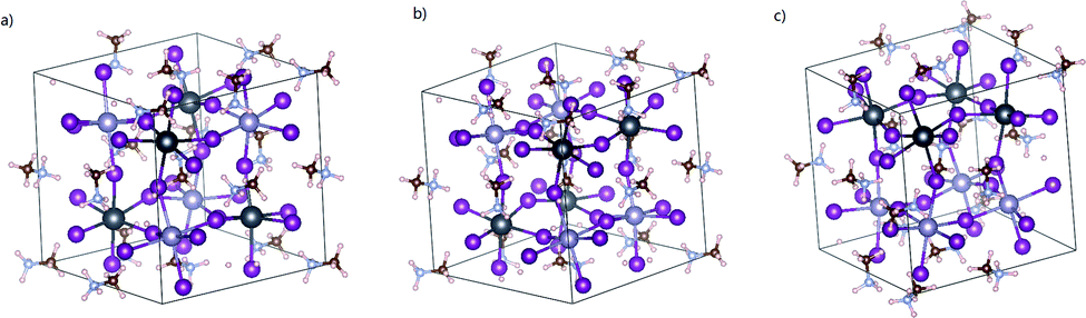 | ||
| Fig. 1 Optimized structure of mixed Pb–Sn perovskite MA2SnPbI6. | ||
| Structures | (a) | (b) | (c) |
|---|---|---|---|
| a/Å | 12.25 | 11.74 | 11.16 |
| bÅ | 12.23 | 12.25 | 12.20 |
| c/Å | 12.28 | 12.28 | 12.21 |
| Free energy/eV | −417.302 | −417.303 | −417.360 |
The influence of VPb, VSn, and iI on the structure of MA2SnPbI6 is then explored. All the defective structures are relaxed with the lattice parameters fixed at the defect-free values to simulate point defects in a bulk crystal. To describe the influence of the defects on the system's geometry, we show the topological structure parameters of the defect-adjacent atoms in the flawed structures in Fig. 2 and Table 2, which demonstrate that when VPb or VSn appears, the average Sn–I bond lengths are longer than those without any defect. Thus, the atoms around the vacancies tend to move backwards the defect sites, so that the [SnI6]4− octahedra are strongly distorted to accommodate these inert defects. However, it has weaker effect towards the structure of [PbI6]4− octahedra. In addition, the vacancy defects flatten the metal-halide framework, as manifested in the increase of the average ∠M–X–M angles. For the iI structure, the atoms around iI are pulled away from the point defect by the adjacent framework, as reflected by the shorter bond lengths, smaller bond angles and distortion of M–X octahedral coordination.
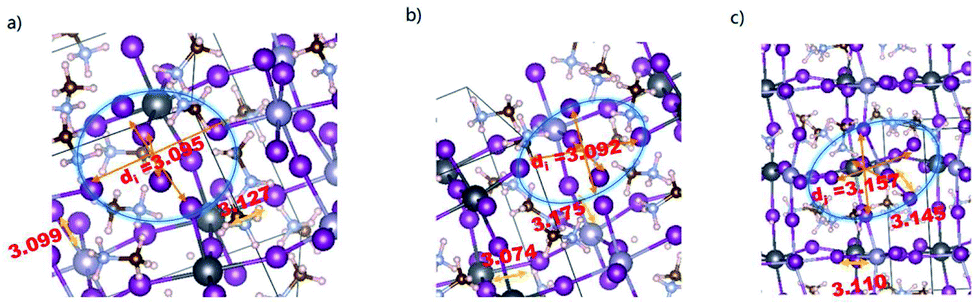 | ||
| Fig. 2 Optimized defect-bearing structures of the MA2SnPbI6 perovskites: (a) VPb, (b) VSn and (c) iI. | ||
![[d with combining macron]](https://www.rsc.org/images/entities/i_char_0064_0304.gif) i denotes the average distance for the vacancy-sharing atoms in the flawed crystal
i denotes the average distance for the vacancy-sharing atoms in the flawed crystal
| Structures | Pristine | VSn | VPb | iI |
|---|---|---|---|---|
| d Sn–I/Å | 3.134 | 3.175 | 3.099 | 3.110 |
| d Pb–I/Å | 3.185 | 3.074 | 3.127 | 3.145 |
| ∠Sn–I–Sn/° | 154.2 | 161.1 | 156.4 | 147.2 |
| ∠Pb–I–Pb/° | 153.5 | 165.6 | 167.8 | 153.2 |
| min(∠M–X–M)° | 148.6 | 146.6 | 148.2 | 108.2 |
|
i
/Å |
— | 3.092 | 3.095 | 3.157 |
| DFE/(eV per cell) | — | +0.294 | +0.128 | +0.045 |
The formalism of DFE allows calculation of defect and impurity equilibrium structures and concentrations, and the relative stability of the different charge states of a given defect in the crystals.75 We also calculated the relative DFEs of those point defects (see Table 2). The DFEs of charged defects are affected by the Fermi energy and the valence band level. The DFEs are expressed as76 DFE = Edefected − (Eperfect + ∑εi,dopants) + q(Ef + VBM + ΔVcorr) + Vcorr, in which, Ef represents the Fermi energy, and ΔVcorr means the VBM potential correction with the bulk flawless phase reference. q denotes the charge state of a defect: for a neutral defect, q = 0, and if the defect structure has a positive charge, q = 1. Vcorr is set for the electrostatic interaction correction between charged point defects in the periodically repeated supercells. In this work, the Makov–Payne approach77 with the monopole approximation, 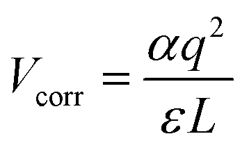 , is adopted to calculate this term, in which the constant α represents the Madelung factor,78–80 and ε is the dielectric constant obtained from the density functional perturbation theory.81,82 The calculated DFEs demonstrate that iI is generated most easily, followed by VPb and VSn. When a Sn(II) cation gets oxidized to Sn(IV), vacancy formation in the adjacent Pb(II) atoms is more likely than that in the Sn(II) atoms.
Considering that the intrinsic defects in actual system are often scattered in the lattice, we build a structure expressed as MASn0.03125Pb0.96875I3, which possesses a large unit cell constructed by setting the minimum unit cell of MA2SnPbI6 shown in Fig. 1(c) in the center and surrounding it by the high-stability MAPbI3 (see Fig. S1†). Then we investigated the influence of three kinds of point defects on the topological structure and calculate DFEs. The data shown in Table 2 and S1† tell that the influence of internal defects on MA2SnPbI6 and MASn0.03125Pb0.96875I3 is consistent. However, the defect-induced deformation on the MASn0.03125Pb0.96875I3 lattice is slightly weaker than that on the MA2SnPbI6 lattice because of the tolerance of a large amount of stable MAPbI3 in the former. The tolerance effect of the surrounding protective layer on the bond length of the defect-sharing atoms is less than 3%, indicating that the deformation on the defect-sharing structure is not affected by the lattice size. Therefore, to achieve a better balance between the computational cost and accuracy, we adopt the MA2SnPbI6 structure for later study.
3.2 Electronic and optoelectronic properties
Before NAMD calculations and carrier recombination analysis, we first make a static energy band analysis of the electronic structure. The band structure and projected density-of-states (pDOSs) of MA2SnPbI6 with and without the defects are plotted in Fig. 4 and S3–S5.†The calculated band gap of MA2SnPbI6 is between those of MAPbI3 (1.57 eV) and MASnI3 (1.28 eV) by HSE06 + SOC, attributed to the hybridization of inert Pb-6s orbitals (with a minor 6p contribution) and active Sn-5s orbitals (with a minor 5p contribution) in the VBM. The CBM of MA2SnPbI6 is also composed of Pb-6p, Sn-5p and I-5p. iI creates a characteristic deep defect state (DDS) lying in the band gap near the Fermi level, which is 0.43 eV above the VBM, and 0.26 eV below the CBM. This DDS is composed of the I-5p orbital of the interstitial I−, and its energy dispersion E(k) is nearly flat.
The characteristic defect states created by VPb and VSn are located below the VBMs, and they thus do not change the width of the band gap. However, the vacancies create several impurity states under the VBM and change the energy dispersions, indicating that they will play a role in the carrier migration and recombination. The pDOS in Fig. S3† shows that VSn weakens the contribution of Sn-5s to the VBM and CB edge states, while VPb had no such severe influence. The contribution of Pb-6s orbitals to the pDOS starts at lower energies compared to Sn-5s, and therefore, the influence of VPb on the VBM near the Fermi level is weaker than that of VSn. The charge distributions of the pristine and flawed MA2SnPbI6 are shown in Fig. S4.†
The relative mobility of the charge carriers can be characterized by the carrier effective masses.83,84 The effective masses are calculated by fitting the energy dispersions of the VBM and the CBM to quadratic functions as  , where mxx, myy, and mzz correspond to the components in the x, y, and z directions, respectively. The results calculated for MA2SnPbI6 with and without defects are shown in Fig. 3(b).
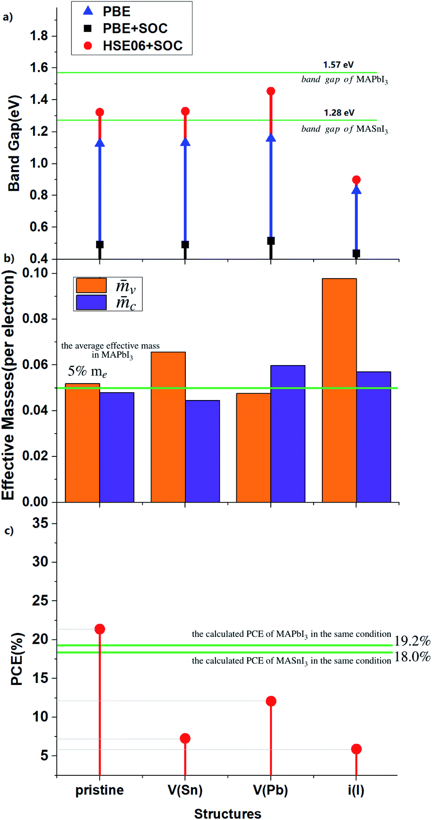 | ||
| Fig. 3 (a) Band gaps calculated by PBE, PBE + SOC and HSE06 + SOC. (b) Effective masses and (c) PCEs calculated by PBE + SOC for the perfect and defective MA2SnPbI6. Comparison is made with the pure Pb-based and Sn-based perovskites. | ||
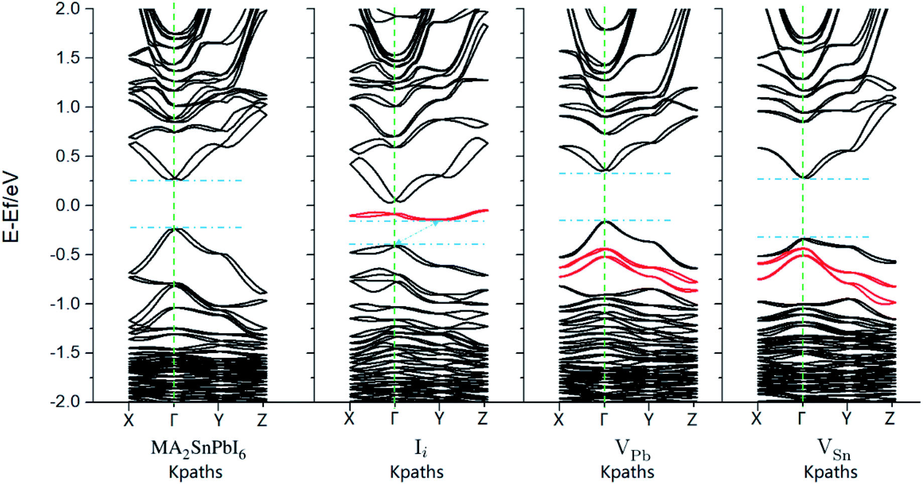 | ||
| Fig. 4 Band structure of MA2SnPbI6 (a) without and (b–d) with intrinsic defects calculated by PBE + SOC. The red lines highlight the bands created by the intrinsic defects. | ||
When Sn atoms are present in the structure, the effective electron mass of the CBM (![[m with combining macron]](https://www.rsc.org/images/entities/i_char_006d_0304.gif) c) is very close to or even slightly lower than that of the pure Pb-based perovskite (approx. 5%85), indicating higher electron carrier mobility. Introduction of VPb and iI can inhibit the electron mobility to a certain extent, and VSn has no obvious effect on it. In addition, these intrinsic defects have a significant impact on the hole mass in the VBM (v), especially iI.
c) is very close to or even slightly lower than that of the pure Pb-based perovskite (approx. 5%85), indicating higher electron carrier mobility. Introduction of VPb and iI can inhibit the electron mobility to a certain extent, and VSn has no obvious effect on it. In addition, these intrinsic defects have a significant impact on the hole mass in the VBM (v), especially iI.
VSn and VPb insert defect states below the VBM, and increase the energy dispersion of the VBM without changing the band gap magnitude. Since the VBMs arise mainly from the Sn-5s orbitals, VSn reduces the VBM dispersion more significantly. In other words, vacancy defects, such as VSn and VPb, make the VBM more localized.
The band gap is a key property of a light-to-energy conservation device, putting limits on its efficiency. Photons with a lower energy than the band gap cannot be absorbed efficiently, while electron–hole pairs generated above the band gap usually relax to the band edges, so that only part of the absorbed energy can be turned into work. In this sense, the absorption spectrum directly determines the PCE value. Hereafter, we adopt the spectral-limited maximum efficiency method as the PCE descriptor, going beyond the band gap, as suggested by Yu and Zunger86,87 to calculate the number of photons absorbed by each structure. The efficiency, η, is obtained as 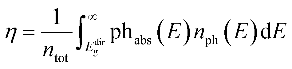 . Here, ntot is the total number of photons emitted by the sun at AM1.5,88 phabs(E) is the photon absorptivity characteristic of the material, and nph(E) represents the number of sun photons at the energy, E, in the unit of eV. In this model, no absorption occurs below the direct bandgap, Edirg, since absorption through an indirect transition requires a change in the electron momentum assisted by phonons.
The calculated PCEs of the materials under investigation corresponding to the same optoelectronic device thickness (shown in Fig. S6†) are shown in Fig. 3(c) and S5 and S6.† The calculated results show that the band gap of pristine MA2SnPbI6 is closer to the Shockley–Queisser limit value of 1.37 eV (ref. 89) than the MAPbI3 and MASnI3 band gaps. Therefore, it exhibits higher PCE. All three point defects decrease the PCE. VPb has the weakest impact on the electronic structure and PCE. VSn decreases the PCE more than VPb. The DDS induced by iI greatly changes the band structure and has the most serious impact on the PCE.
3.3 Electron–hole recombination and hot electron relaxation
In order to quantitatively describe the influence of the intrinsic defects on the carrier lifetimes, we have performed a series of NAMD simulations on the photexcited carrier relaxation and electron–hole recombination processes for the perfect and defective structures. Considering the computational effort, the NAMD simulations are based on the PBE functional without SOC since the band gaps calculated by PBE without SOC are much closer to those obtained by HSE06 + SOC than the band gaps obtained by PBE + SOC, and NAMD calculations based on HSE06 + SOC are too computationally demanding. The calculated non-adiabatic coupling (NAC) matrices are shown in Fig. S7.†
Fig. 5 shows the pure-dephasing functions calculated using the second order cumulant expansion as  . This optical response function characterizes the vibrationally induced pure-dephasing process for a pair of states entangled in a coherent superposition. It can be obtained directly or via the second-order cumulant expansion,90 which allows notably better convergence. Pure-dephasing is associated with fluctuations of electronic energy levels due to coupling to phonons. The fluctuations are characterized by the energy gap autocorrelation function (ACF). The un-normalized ACF is defined as C(t) = 〈ΔE(t)ΔE(0)〉. It represents an ensemble average of the correlation of the energy gap fluctuation. A rapid decay of the ACF implies fast pure-dephasing. The ACFs characterize memory of the energy gap fluctuation.
 | ||
| Fig. 5 Calculated pure-dephasing function of MA2SnPbI6 with and without defects. The result comparison is made with MAPbI3. | ||
Generally, shorter pure-dephasing time leads to slower dynamics, as exemplified by the quantum Zeno effect.91 The pure-dephasing times depend most strongly on the magnitude of the phonon-induced fluctuation of the corresponding electronic energy gap.92 Fig. S8(a)† shows the un-normalized ACF of the energy gap fluctuation, and the ACF initial values characterize the fluctuation magnitude. The fluctuation is the largest for the pristine system, resulting in the fastest decay of the pure-dephasing function. The iI defect exhibits slower pure-dephasing, because the corresponding energy gap and its fluctuation are the smallest.
Fourier transform of the ACF produces the spectral density  . As shown in Fig. S8(b),† the calculated spectral densities characterize the phonon modes that couple to the electronic subsystem. Low-frequency modes play a predominant role, corresponding to twisting and stretching motion of the [PbI6]4− and [SnI6]4− octahedra, according to the previous research.93,94
To determine the time scales τ of the non-radiative electron–hole recombination, we obtain 30 ps of NAMD data, and fit the state populations to the short-time, linear approximation of exponential decay, i.e., P(t) = exp(−t/τ) ≈ 1 − t/τ. Table 3 demonstrates that the carrier lifetime of the MA2SnPbI6 mixed perovskite is between those of MAPbI3 and MASnI3. Due to the higher VBM energy, pristine MA2SnPbI6 possesses a smaller band gap, and therefore, exhibits a shorter carrier lifetime than MAPbI3. On the other hand, the incorporation of Pb into the Sn-based perovskite increases the carrier lifetime compared with that of the pure Sn-based perovskite. All the defective MA2SnPbI6 perovskites exhibit shorter carrier lifetimes than the pristine system. This can be traced to smaller initial values of the unnormalized ACF and longer pure-dephasing times. The carrier lifetimes of the perovskites with the cation vacancies are shorter because the VBM state is mixed with the defect states formed in the VB, Fig. 6(a). The VSn defect influences the electronic states near the VBM more strongly than the VPb defect, because it is energetically closer to the VBM, and notably hybridizes the VBM and deeper VB state, Fig. S3.† As a result, VSn changes the nonradiative charge recombination between the VBM and CBM more significantly than VPb. Changes in the spatial distributions of charges near the VBM and the CBM, Fig. S4,† are an important reason for variation of the carrier lifetime in different structures.96
| Structure | SnPb | VPb | VSn | iI | all-Pb | all-Sn95 |
|---|---|---|---|---|---|---|
| τ/ns | 54.88 | 20.11 | 5.72 | 0.441 | 159.6 | 8.37 |
 | ||
| Fig. 6 Electron–hole recombination process from the CBM to the VBM for MA2SnPbI6 with and without defects. | ||
The iI-bearing system exhibits much faster nonradiative carrier recombination than the other systems studied in this work, Fig. 6. The DDS plays a decisive role here. The iI creates DDS, Fig. 4(a), splitting the band gap into two smaller gaps, 0.43 eV + 0.26 eV by PBE + SOC. Nonradiative transitions across small energy gaps are fast, resulting in quick carrier quenching. 32% of active carriers recombine within the 30 ps NAMD simulation and 14% of them are captured by the interstitial DDS, Fig. 6(b).
To unveil the effect of these point defects on the carrier relaxation process, we simulate the hot electron relaxation dynamics from the low-lying CB edge states to the CBM, as shown in Fig. 7. Considering hot charge carriers at energies away from the band edges can provide advantages in solar energy applications, such as faster charge separation and transport, generation of additional carriers, and reduced trapping,97 here we include all the relaxation effects from CBM + 1, CBM + 2 and CBM + 3 to the CBM.
 | ||
| Fig. 7 Hot electron relaxation process from CBM + 1, CBM + 2 and CBM + 3 to the CBM for MA2SnPbI6 with and without defects. | ||
The CB edges are mainly composed of Sn-5s 5p and Pb-6s6p orbitals (see Fig. S3†). Therefore, VPb and VSn significantly weaken the contribution of Pb and Sn to CB edges, leading to the increase of the relaxation time. The calculated carrier relaxation times τ for the VPb- and VSn-bearing structures are 2.02 and 1.29 ps, respectively. Because the iI defect creates the mid-gap states and hardly affects the deep CB states, the carrier relaxation time of the iI-bearing structure (τ = 0.97 ps) is nearly the same as that of the defect-free structure (τ = 1.01 ps).
4 Concluding remarks
We have performed first-principles DFT calculations combined with NAMD simulations on the static and dynamic characteristics of MA2SnPbI6 with and without intrinsic point defects, and compared its properties with those of its pure counterparts MASnI3 and MAPbI3. Meantime, in order to discuss the stability of defects in the realistic system as accurately as possible, we also calculated the geometric structures and defect formation energies of MASn0.03125Pb0.96875I3 with a large supercell. This study unveils the nature of defect states and reveals how the intrinsic defects in the mixed Pb–Sn perovskite frameworks affect the electronic and geometric structures, the electron-vibrational coupling, the hot electron relaxation times, and the times of the nonradiative electron–hole recombination process at the ambient temperature. The following conclusions can be extracted from this study.(1) The oxidation of Sn(II) results in the generation of many intrinsic defects such as VSn, VPb and iI in the MA2SnPbI6 material. iI can be most easily generated, followed by VPb and VSn. When one Sn(II) atom is oxidized, its adjacent Pb(II) atoms are prone to forming a defective vacancy, prior to Sn(II) atoms, and once a defect appears nearby, the [SnI6]4− octahedra are always distorted more severely than [PbI6]4− octahedra. It has been noted that Sn–Pb mixed perovskite materials possess an important feature: when Sn(II) is oxidized to Sn(IV), an adjacent Pb-vacancy forms, which will partially tolerate the negative impact of Sn(IV) on the photoelectric properties of Sn–Pb mixed perovskite materials.
(2) VPb, VSn and iI affect the crystal structure differently. VPb and VSn cause elongation and distortion of the MX octahedra around the defects. This is reflected in a displacement of the octagon geometric centers. The M–X bond lengths of the center ion increase to offset somewhat the distortion of the octahedral structure. iI makes the two adjacent MX octahedra repel each other, manifested in the reduction of the M–X bond lengths. Additionally, the vacancy defects flatten the M–X framework, while iI distorts it severely.
(3) The band gap width and the carrier lifetime of MA2SnPbI6 lie between those of MAPbI3 and MASnI3 because the orbital hybridization of Sn and Pb affects the energy level of its VBMs, which are composed of the Sn-5s5p and Pb-6s6p orbitals. MA2SnPbI6 exhibits higher PCE than MAPbI3 and MASnI3 because its band gap width is much closer to the Shockley–Queisser limit. The tolerance of Pb-vacancy defects by the mixed Pb–Sn perovskite is also reflected in the electronic structure. The CBMs of MA2SnPbI6 are predominantly composed of the Sn-5p orbitals so that removing a Pb atom has a nearly negligible impact on its CB-related properties. Therefore, we can conclude that the existence of Pb atoms can inhibit the degradation arising from Sn oxidation in MA2SnPbI6. This is of great significance for maintaining the photoelectric activity of Sn-bearing perovskites.
(4) The point defects shorten the carrier lifetime of the material in the following order, VPb, VSn and iI, with iI giving the fastest carrier losses. The iI defect creates deep defect states in the middle region of the band gap, which introduce new carrier recombination pathways, leading to a significant decrease of the carrier lifetime and the PCE. 32% of the carriers are lost within 30 ps due to the nonradiative electron–hole recombination in the presence of iI and 14% of them are captured by the deep defect states created by the iI defect. In order to avoid formation of the iI defects, we suggest to decrease the anion content, or increase the cation content, to prevent the generation of iI during nucleation of the crystal. Both VSn and VPb do not create defect levels in the band gap. However, they alter the energy dispersions of both the VBM and the CBM, changing the carriers' mobility and lifetime. The VSn defect weakens hybridization of the Pb and Sn orbitals, such that the Sn-5s and 5p orbitals contribute to the VBM very weakly around the defect. VPb has less impact on the material than VSn, because Pb atoms contribute less to the VBM edge states.
(5) Contrary to their influences on the electron–hole recombination process, the three kinds of point defects exhibit an impact on the hot carrier relaxation process with the order of iI, VSn and VPb. iI hardly affects the relaxation and both VPb and VSn slow down the relaxation, attributed to the defect-induced different changes on the energy dispersions of CB edge states.
This study establishes the microscopic mechanisms underlying the simultaneous improvement of the perovskite stability and the charge carrier lifetime by the hybrid cation strategy. It reveals the nature of the defect states and the influence of the intrinsic defects on the structures and optoelectronic properties, as well as the charge carriers' mobility and lifetimes. The general and fundamental principles established by analysis of the simulation results are useful for design of advanced materials for solar energy and optoelectronic applications.
Conflicts of interest
There are no conflicts to declare.Acknowledgements
Financial support from the National Natural Science Foundation of China (Grant Nos 21833006 and 22173074) and the USA National Science Foundation (Grant No. CHE-1900510) is acknowledged.Notes and references
- A. Jena, A. Kulkarni and T. Miyasaka, Halide Perovskite Photovoltaics: Background, Status, and Future Prospects, Chem. Rev., 2019, 119, 3036–3103 CrossRef CAS.
- S. D. Stranks and H. J. Snaith, Metal-Halide Perovskites for Photovoltaic and Light-Emitting Devices, Nat. Nanotechnol., 2015, 10, 391–402 CrossRef CAS.
- A. Kojima, K. Teshima, Y. Shirai and T. Miyasaka, Light Sensitizers for Photovoltaic Cells, J. Am. Chem. Soc., 2009, 131, 6050–6051 CrossRef CAS.
- J. H. Noh, S. H. Im, J. H. Heo, T. N. Mandal and S. I. Seok, Chemical Management for Colorful, Efficient, and Stable Inorganic-Organic Hybrid Nanostructured Solar Cells, Nano Lett., 2013, 13, 1764–1769 CrossRef CAS PubMed.
- W. Yu, F. Li, L. Yu, M. R. Niazi, Y. Zou, D. Corzo, A. Basu, C. Ma, S. Dey, M. L. Tietze, T. Wu and A. Amassian, Single Crystal Hybrid Perovskite Field-Effect Transistors, Nat. Commun., 2018, 9, 1–10 CrossRef.
- J. Huang, Y. Yuan, Y. Shao and Y. Yan, Understanding the Physical Properties of Hybrid Perovskites for Photovoltaic Applications, Nat. Rev. Mater., 2017, 2, 17042–17119 CrossRef CAS.
- M. Grätzel, The Light and Shade of Perovskite Solar Cells, Nat. Mater., 2014, 13, 838–842 CrossRef PubMed.
- National Renewable Energy Laboratory, Best Research-Cell Efficiencies, http://www.nrel.gov/pv/cell-efficiency.html, 2021 Search PubMed.
- M. Lira-Cantu, Stability Lies at Interfaces, Nat. Energy, 2017, 2, 17115 CrossRef.
- S. Battersby, The Solar Cell of the Future, Proc. Natl. Acad. Sci., 2019, 116, 7–10 CrossRef CAS PubMed.
- S. Chen, Y. Deng, H. Gu, S. Xu, S. Wang, Z. Yu, V. Blum and J. Huang, Trapping lead in perovskite solar modules with abundant and low-cost cation-exchange resins, Nat. Energy, 2020, 5, 1003–1011 CrossRef.
- P. P. Boix, S. Agarwala, T. M. Koh, N. Mathews and S. G. Mhaisalkar, Perovskite Solar Cells: Beyond Methylammonium Lead Iodide, J. Phys. Chem. Lett., 2015, 6, 898–907 CrossRef CAS PubMed.
- C. Liu, W. Li, J. Fan and Y. Mai, A brief review on the lead element substitution in perovskite solar cells, J. Energy Chem., 2018, 27, 1054–1066 CrossRef.
- V. K. Ravi, B. Mondal, V. V. Nawale and A. Nag, Don't Let the Lead Out: New Material Chemistry Approaches for Sustainable Lead Halide Perovskite Solar Cells, ACS Omega, 2020, 5, 29631–29641 CrossRef CAS.
- F. Giustino and H. J. Snaith, Toward Lead-Free Perovskite Solar Cells, ACS Energy Lett., 2016, 9, 1233–1240 CrossRef.
- Y. Fang, S. Zhai, L. Chu and J. Zhong, Advances in Halide Perovskite Memristor from Lead-Based to Lead-Free Materials, ACS Appl. Mater. Interfaces, 2021, 13, 17141–17157 CrossRef CAS.
- F. Hao, C. C. Stoumpos, Z. Liu, R. Chang and M. G. Kanatzidis, Controllable Perovskite Crystallization at a Gas-Solid Interface for Hole Conductor-Free Solar Cells with Steady Power Conversion Efficiency over 10%, Nat. Photonics, 2014, 8, 489–494 CrossRef CAS.
- N. K. Noel, S. D. Stranks, A. Abate, C. Wehrenfennig, S. Guarnera, A. A. Haghighirad, A. Sadhanala, G. E. Eperon, S. K. Pathak and M. B. Johnston, et al., Lead-free Organic-Inorganic Tin Halide Perovskites for Photovoltaic Applications, Energy Environ. Sci., 2014, 7, 3061–3068 RSC.
- A. H. Slavney, T. Hu, A. M. Lindenberg and H. T. Karunadasa, A Bismuth-Halide Double Perovskite with Long Carrier Recombination Lifetime for Photovoltaic Applications, J. Am. Chem. Soc., 2016, 138, 2138–2141 CrossRef CAS.
- E. T. McClure, M. R. Ball, W. Windl and P. M. Woodward, Cs2AgBiX6 (X = Br, Cl): New Visible Light Absorbing, Lead-Free Halide Perovskite Semiconductors, Chem. Mater., 2016, 28, 1348–1354 CrossRef CAS.
- G. Volonakis, M. R. Filip, F. Giustino, A. A. Haghighirad, N. Sakai, B. Wenge and H. J. Snaith, Lead-Free Halide Double Perovskites via Heterovalent Substitution of Noble Metals, J. Phys. Chem. Lett., 2016, 7, 1254–1259 CrossRef CAS PubMed.
- F. Wei, Z. Deng, S. Sun, F. Xie, G. Kieslich, D. M. Evans, M. A. Carpenter, P. D. Bristowea and A. K. Cheethama, The Synthesis, Structure and Electronic Properties of a Lead-Free Hybrid Inorganic–Organic Double Perovskite (MA)2KBiCl6 (MA = methylammonium), Mater. Horiz., 2016, 3, 328–332 RSC.
- M. R. Filip, S. Hillman, A. A. Haghighirad, H. J. Snaith and F. Giustino, Band Gaps of the Lead-Free Halide Double Perovskites Cs2BiAgCl6 and Cs2BiAgBr6 from Theory and Experiment, J. Phys. Chem. Lett., 2016, 7, 2579–2585 CrossRef CAS PubMed.
- Z. Deng, F. Wei, S. Sun, G. Kieslich, A. K. Cheetham and P. D. Bristowe, Exploring the Properties of Lead-Free Hybrid Double Perovskites Using a Combined Computational-Experimental Approach, J. Mater. Chem. A, 2016, 4, 12025–12029 RSC.
- Y. J. Li, T. Wu, L. Sun, R. X. Yang, L. Jiang, P. F. Cheng, Q. Q. Hao, T. J. Wang, R. F. Lu and W. Q. Deng, Lead-free and Stable Antimony-Silver-Halide Double Perovskite (CH3NH3)2AgSbI6, RSC Adv., 2017, 7, 35175–35180 RSC.
- M. Pazoki, M. B. Johansson, H. Zhu, P. Broqvist, T. Edvinsson, G. Boschloo and E. M. Johansson, Bismuth Iodide Perovskite Materials for Solar Cell Applications: Electronic Structure, Optical Transitions, and Directional Charge Transport, J. Phys. Chem. C, 2016, 120, 29039–29046 CrossRef CAS.
- G. Volonakis, A. A. Haghighirad, R. L. Milot, W. H. Sio, M. R. Filip, B. Wenger, M. B. Johnston, L. M. Herz, H. J. Snaith and F. Giustino, Cs2InAgCl6: A New Lead-Free Halide Double Perovskite with Direct Band Gap, J. Phys. Chem. Lett., 2017, 8, 772–778 CrossRef CAS PubMed.
- B. Yang, J. Chen, S. Yang, F. Hong, L. Sun, P. Han, T. Pullerits, W. Deng and K. Han, Lead-Free Silver-Bismuth Halide Double Perovskite Nanocrystals, Angew. Chem., Int. Ed., 2018, 57, 5359–5363 CrossRef CAS PubMed.
- X. G. Zhao, J. H. Yang, Y. Fu, D. Yang, Q. Xu, L. Yu, S. H. Wei and L. Zhang, Design of Lead-Free Inorganic Halide Perovskites for Solar Cells via Cation-Transmutation, J. Am. Chem. Soc., 2017, 139, 2630–2638 CrossRef CAS.
- A. H. Slavney, L. Leppert, A. Saldivar Valdes, D. Bartesaghi, T. J. Savenije, J. B. Neaton and H. I. Karunadasa, Small-Band-Gap Halide Double Perovskites, Angew. Chem., Int. Ed., 2018, 57, 12765–12770 CrossRef CAS.
- X. Zhao, D. Yang, Y. Sun, T. Li, L. Zhang, L. Yu and A. Zunger, Cu–In Halide Perovskite Solar Absorbers, J. Am. Chem. Soc., 2017, 139, 6718–6725 CrossRef CAS PubMed.
- Q. Liu and W. Z. Liang, Structure and property tunability in monolayer halide lead-free double hybrid perovskites: effects of Rashba and biaxial strain, J. Mater. Chem. A, 2019, 7, 11487–11496 RSC.
- M. Pantaler, K. Cho, V. Queloz, B. Garcia, C. Fettkenhauer, I. Anusca, M. Nazeeruddin, D. Lupascu and G. Grancini, Hysteresis-Free Lead-Free Double-Perovskite Solar Cells by Interface Engineering, ACS Energy Lett., 2018, 3, 1781–1786 CrossRef CAS.
- M. R. Filip, S. Hillman, A. A. Haghighirad, H. J. Snaith and F. Giustino, Band Gaps of the Lead-Free Halide Double Perovskites Cs2BiAgCl6 and Cs2BiAgBr6 from Theory and Experiment, J. Phys. Chem. Lett., 2016, 7, 2579–2585 CrossRef CAS PubMed.
- G. Volonakis, A. A. Haghighirad, H. J. Snaith and F. Giustino, Route to Stable Lead-Free Double Perovskites with the Electronic Structure of CH3NH3PbI3: A Case for Mixed-Cation Cs/CH3NH3/CH(NH2)22InBiBr6, J. Phys. Chem. Lett., 2017, 8, 3917–3924 CrossRef CAS PubMed.
- K. McCall, D. Friedrich, D. Chica, W. Cai, C. Stoumpos, G. Alexander, S. Deemyad, B. Wessels and M. Kanatzidis, Perovskites with a Twist: Strong In1+ Off-Centering in the Mixed-Valent CsInX3 (X = Cl, Br), Chem. Mater., 2019, 31, 9554–9566 CrossRef CAS.
- W. Zhu, G. Xin, Y. Wang, X. Min, T. Yao, W. Xu, M. Fang, S. Shi, J. Shi and J. Lian, Tunable optical properties and stability of lead free all inorganic perovskites Cs2SnIxCl6−x, J. Mater. Chem. A, 2018, 6, 2577–2584 RSC.
- M. G. Ju, J. Dai, L. Ma and X. C. Zeng, Lead-Free Mixed Tin and Germanium Perovskites for Photovoltaic Application, J. Am. Chem. Soc., 2017, 139, 8038–8043 CrossRef CAS.
- C. Stoumpos, L. Frazer, D. Clark, Y. Kim, S. Rhim, A. Freeman, J. Ketterson, J. Jang and M. G. Kanatzidis, Hybrid Germanium Iodide Perovskite Semiconductors: Active Lone Pairs, Structural Distortions, Direct and Indirect Energy Gaps, and Strong Nonlinear Optical Properties, J. Am. Chem. Soc., 2015, 137, 6804–6819 CrossRef CAS.
- I. Kopacic, B. Friesenbichler, S. Hoefler, B. Kunert, H. Plank, T. Rath and G. Trimmel, Enhanced Performance of Germanium Halide Perovskite Solar Cells through Compositional Engineering, ACS Appl. Energy Mater., 2018, 1, 343–347 CrossRef CAS.
- D. Umadevi and G. Watson, Quasiparticle GW Calculations on Lead-Free Hybrid Germanium Iodide Perovskite CH3NH3GeI3 for Photovoltaic Applications, ACS Omega, 2019, 4, 5661–5669 CrossRef CAS.
- T. B. Song, T. Yokoyama, C. C. Stoumpos, J. Logsdon, D. H. Cao, M. R. Wasielewski, S. Aramaki and M. G. Kanatzidis, Importance of Reducing Vapor Atmosphere in the Fabrication of Tin-Based Perovskite Solar Cells, J. Am. Chem. Soc., 2017, 139, 836–842 CrossRef CAS.
- A. Stroppa, D. Di Sante, P. Barone, M. Bokdam, G. Kresse, C. Franchini, M. H. Whangbo and S. Picozzi, Tunable Ferroelectric Polarization and its Interplay with Spin-Orbit Coupling in Tin Iodide Perovskites, Nat. Commun., 2014, 5, 5900 CrossRef CAS.
- D. B. Mitzi, C. A. Feild and W. T. Harrison, Conducting Tin Halides with a Layered Organic-Based Perovskite Structure, Nature, 1994, 369, 467–469 CrossRef CAS.
- A. Goyal, S. McKechnie, D. Pashov, W. Tumas, M. van Schilfgaarde and V. Stevanovic, Origin of Pronounced Nonlinear Band Gap Behavior in Lead–Tin Hybrid Perovskite Alloys, Chem. Mater., 2018, 30, 3920–3928 CrossRef CAS.
- T. Nakamura, T. Handa, R. Murdey, Y. Kanemitsu and A. Wakamiya, Materials Chemistry Approach for Efficient Lead-Free Tin Halide Perovskite Solar Cells, ACS Appl. Electron. Mater., 2020, 2, 3794–3804 CrossRef CAS.
- D. Ramirez, K. Schutt, Z. Wang, A. J. Pearson, E. Ruggeri, H. J. Snaith, S. D. Stranks and F. Jaramillo, Layered Mixed Tin–Lead Hybrid Perovskite Solar Cells with High Stability, ACS Energy Lett., 2018, 3, 2246–2251 CrossRef CAS.
- G. Kapil, T. S. Ripolles, K. Hamada, Y. Ogomi, T. Bessho, T. Kinoshita, J. Chantana, K. Yoshino, Q. Shen, T. Toyoda, T. Minemoto, T. N. Murakami, H. Segawa and S. Hayase, Highly Efficient 17.6% Tin–Lead Mixed Perovskite Solar Cells Realized through Spike Structure, Nano Lett., 2018, 18, 3600–3607 CrossRef CAS PubMed.
- L. Lanzetta, N. Aristidou and S. A. Haque, Stability of Lead and Tin Halide Perovskites: The Link between Defects and Degradation, J. Phys. Chem. Lett., 2020, 11, 574–585 CrossRef CAS.
- R. Shi and R. Long, Hole Localization Inhibits Charge Recombination in Tin–Lead Mixed Perovskites: Time–Domain ab Initio Analysis, J. Phys. Chem. Lett., 2019, 10, 6604–6612 CrossRef CAS PubMed.
- N. L. Lanzetta, N. Aristidou and S. A. Haque, Stability of Lead and Tin Halide Perovskites: The Link between Defects and Degradation, J. Phys. Chem. Lett., 2020, 11, 574–585 CrossRef.
- B. Li, B. Chang, L. Pan, Z. Li, L. Fu, Z. He and L. Yin, Tin-Based Defects and Passivation Strategies in Tin-Related Perovskite Solar Cells, ACS Energy Lett., 2020, 5, 3752–3772 CrossRef CAS.
- D. Son, S. Kim, J. Seo, S. Lee, H. Shin, D. Lee and N. Park, Universal Approach toward Hysteresis-Free Perovskite Solar Cell via Defect Engineering, J. Am. Chem. Soc., 2018, 140, 1358–1364 CrossRef CAS PubMed.
- S. Wang, Y. Jiang, E. Juarez-Perez, L. Ono and Y. Qi, Accelerated degradation of methylammonium lead iodide perovskites induced by exposure to iodine vapour, Nat. Energy, 2017, 2, 16195 CrossRef CAS.
- W. Yin, T. Shi and Y. Yan, Unusual defect physics in CH3NH3PbI3 perovskite solar cell absorber, Appl. Phys. Lett., 2014, 104, 063903 CrossRef.
- Q. Liu and W. Z. Liang, How the Structures and Properties of Pristine and Anion Vacancy Defective Organic–Inorganic Hybrid Double Perovskites MA2AgIn(BrxI1−x)6 Vary with Br Content x, J. Phys. Chem. Lett., 2020, 11, 10315–10322 CrossRef CAS.
- W. Li, Y. She, A. S. Vasenko and O. V. Prezhdo, Ab initio nonadiabatic molecular dynamics of charge carriers in metal halide perovskites, Nanoscale, 2021, 13, 10239–10265 RSC.
- W. Chu, W. A. Saidi, J. Zhao and O. V. Prezhdo, Soft Lattice and Defect Covalency Rationalize Tolerance of β-CsPbI3 Perovskite Solar Cells to Native Defects, Angew. Chem., Int. Ed., 2020, 59, 6435–6441 CrossRef CAS PubMed.
- R. Li, R. Wang, Y. Yuan, J. Ding, Y. Cheng, Z. Zhang and W. Huang, Defect Origin of Emission in CsCu2I3 and Pressure-Induced Anomalous Enhancement, J. Phys. Chem. Lett., 2020, 12, 317–323 CrossRef.
- X. Zhang, Q. Ma, R. Li, C. Lin, D. Huang and Y. Cheng, The mechanism of alkali doping in CsPbBr3: A first-principles perspective, J. Appl. Phys., 2021, 129, 165110 CrossRef CAS.
- Z. Gan, Y. Cheng, W. Chen, K. P. Loh, B. Jia and X. Wen, Photophysics of 2D Organic–Inorganic Hybrid Lead Halide Perovskites: Progress, Debates, and Challenges, Adv. Sci., 2021, 8, 2001843 CrossRef CAS.
- Y. Li, C. Zhang, X. Zhang, D. Huang, Q. Shen, Y. Cheng and W. Huang, Intrinsic point defects in inorganic perovskite CsPbI3 from first-principles prediction, Appl. Phys. Lett., 2017, 111, 162106 CrossRef.
- Z. Nan, L. Chen, Q. Liu, S. Wang, Z. Chen, S. Kang, J. Ji, Y. Tan, Y. Hui, J. Yan, Z. Xie, W. Liang, B. Mao and Z. Tian, Revealing phase evolution mechanism for stabilizing formamidinium-based lead halide perovskites by a key intermediate phase, Chem, 2021, 7, 2513 CAS.
- G. Kresse, Ab-Initio Molecular-Dynamics for Liquid-Metals, J. Non-Cryst. Solids, 1995, 193, 10239–10265 Search PubMed.
- P. E. Blöchl, Projector Augmented-Wave Method, Phys. Rev. B: Condens. Matter Mater. Phys., 1994, 50, 17953–17979 CrossRef PubMed.
- J. P. Perdew, K. Burke and M. Ernzerhof, Generalized Gradient Approximation Made Simple, Phys. Rev. Lett., 1996, 77, 3865–3868 CrossRef CAS PubMed.
- J. Heyd and G. E. Scuseria, Assessment and validation of a screened Coulomb hybrid density functional, J. Chem. Phys., 2004, 120, 7274 CrossRef CAS.
- J. Heyd, G. E. Scuseria and M. Ernzerhof, Hybrid functionals based on a screened Coulomb potential, J. Chem. Phys., 2003, 118, 8207 CrossRef CAS.
- S. Grimme, Semiempirical GGA-type density functional constructed with a long-range dispersion correction, J. Comput. Chem., 2006, 27, 1787–1799 CrossRef CAS.
- S. Grimme, J. Antony, S. Ehrlich and H. Krieg, A consistent and accurate ab initio parametrization of density functional dispersion correction (DFT-D) for the 94 elements H-Pu, J. Chem. Phys., 2010, 132, 154104 CrossRef.
- J. Moellmann and S. Grimme, DFT-D3 Study of Some Molecular Crystals, J. Phys. Chem. C, 2014, 118, 7615–7621 CrossRef CAS.
- T. Verteśi, Á. Vibók, G. J. Halász, A. Yahalom, R. Englman and M. Baer, The Electronic Non-Adiabatic Coupling Matrix: A Numerical Study of the Curl Condition and the Quantization Condition Employing the Mathieu Equation, J. Phys. Chem. A, 2003, 107, 7189–7196 CrossRef.
- A. V. Akimov and O. V. Prezhdo, The PYXAID Program for Non-Adiabatic Molecular Dynamics in Condensed Matter Systems, J. Chem. Theory Comput., 2013, 9, 4959–4972 CrossRef CAS PubMed.
- A. V. Akimov and O. V. Prezhdo, Advanced Capabilities of the PYXAID Program: Integration Schemes, Decoherence Effects, Multiexcitonic States, and Field-Matter Interaction, J. Chem. Theory Comput., 2014, 10, 789–804 CrossRef CAS PubMed.
- C. Freysoldt, B. Grabowski, T. Hickel and J. Neugebauer, First-principles Calculations for Point Defects in Solids, Rev. Mod. Phys., 2015, 86, 253–305 CrossRef.
- D. Meggiolaro and F. de Angelis, First-Principles Modeling of Defects in Lead Halide Perovskites: Best Practices and Open Issues, ACS Energy Lett., 2018, 3, 2206–2222 CrossRef CAS.
- G. Makov and M. C. Payne, Periodic Boundary Conditions in Ab-Initio Calculations, Phys. Rev. B: Condens. Matter Mater. Phys., 1995, 51, 4014–4022 CrossRef CAS.
- B. Nijboer and F. De Wette, On the calculation of lattice sums, Phys. D, 1957, 23, 309–321 CAS.
- L. Glasser, Solid-State Energetics and Electrostatics: Madelung Constants and Madelung Energies, Inorg. Chem., 2012, 51, 2420–2424 CrossRef CAS PubMed.
- R. P. Grosso, J. T. Fermann and W. J. Vining, An In-Depth Look at the Madelung Constant for Cubic Crystal Systems, J. Chem. Educ., 2001, 78, 1198 CrossRef CAS.
- K. Refson, P. Tulip and S. Clark, Variational density-functional perturbation theory for dielectrics and lattice dynamics, Phys. Rev. B: Condens. Matter Mater. Phys., 2006, 73, 155114 CrossRef.
- S. Wu, D. Vanderbilt and D. Hamann, Systematic treatment of displacements, strains, and electric fields in density-functional perturbation theory, Phys. Rev. B: Condens. Matter Mater. Phys., 2005, 72, 035105 CrossRef.
- M. G. Ju, G. X. Sun, Y. Zhao and W. Z. Liang, A Computational View of the Change in the Geometric and Electronic Properties of Perovskites Caused by the Partial Substitution of Pb by Sn, Phys. Chem. Chem. Phys., 2015, 17, 17679–17687 RSC.
- J. Feng and B. Xiao, Effective Masses and Electronic and Optical Properties of Nontoxic MASnX3 (X = Cl, Br, and I) Perovskite Structures as Solar Cell Absorber: A Theoretical Study Using HSE06, J. Phys. Chem. C, 2014, 118, 19655–19660 CrossRef CAS.
- S. Chatterjee and A. Pal, Influence of metal substitution on hybrid halide perovskites: towards lead-free perovskite solar cells, J. Mater. Chem. A, 2018, 6, 3793–3823 RSC.
- L. Yu and A. Zunger, Identification of Potential Photovoltaic Absorbers Based on First-Principles Spectroscopic Screening of Materials, Phys. Rev. Lett., 2012, 108, 068701 CrossRef.
- I. E. Castelli, K. S. Thygesen and K. W. Jacobsen, Calculated optical absorption of different perovskite phases, J. Mater. Chem. A, 2015, 3, 12343–12349 RSC.
- Reference Solar Spectral Irradiance: Air Mass 1.5, http://rredc.nrel.gov/solar/spectra/am1.5/hmtl Search PubMed.
- W. Shockley and H. J. Queisser, Detailed Balance Limit of Efficiency of p–n Junction Solar Cells, J. Appl. Phys., 1961, 32, 510–519 CrossRef CAS.
- S. Mukamel, Principles of Nonlinear Optical Spectroscopy, 1995 Search PubMed.
- S. V. Kilina, A. J. Neukirch, B. F. Habenicht, D. S. Kilin and O. V. Prezhdo, Quantum Zeno effect rationalizes the phonon bottleneck in semiconductor quantum dots, Phys. Rev. Lett., 2013, 110, 180404 CrossRef.
- A. V. Akimov and O. V. Prezhdo, Persistent Electronic Coherence Despite Rapid Loss of Electron-Nuclear Correlation, J. Phys. Chem. Lett., 2013, 4, 3857–3864 CrossRef CAS.
- A. M. Leguy, A. R. Goni, J. M. Frost, J. Skelton, F. Brivio, X. Rodriguez-Martinez, O. J. Weber, A. Pallipurath, M. I. Alonso, M. Campoy-Quiles, M. T. Weller, J. Nelson, A. Walsh and P. R. Barnes, Dynamic disorder, phonon lifetimes, and the assignment of modes to the vibrational spectra of methylammonium lead halide perovskites, Phys. Chem. Chem. Phys., 2016, 18, 27051–27066 RSC.
- C. Quarti, G. Grancini, E. Mosconi, P. Bruno, J. M. Ball, M. M. Lee, H. J. Snaith, A. Petrozza and F. de Angelis, The Raman Spectrum of the CH3NH3PbI3 Hybrid Perovskite: Interplay of Theory and Experiment, J. Phys. Chem. Lett., 2014, 5, 279–284 CrossRef CAS PubMed.
- A. Li, Q. Liu, W. B. Chu, W. Z. Liang and O. V. Prezhdo, Why Hybrid Tin-Based Perovskites Simultaneously Improve the Structural Stability and Charge Carriers-Lifetime: Ab Initio Quantum Dynamics, ACS Appl. Mater. Interfaces, 2021, 13, 16567–16575 CrossRef CAS.
- S. Banerjee, J. Kang, X. Zhang and L. Wang, The effects of interstitial iodine in hybrid perovskite hot carrier cooling: A non-adiabatic molecular dynamics study, J. Chem. Phys., 2020, 152, 091102 CrossRef CAS PubMed.
- T. Wang, L. Jin, J. Hidalgo, W. Chu, J. Snaider, S. Deng, T. Zhu, B. Lai, O. V. Prezhdo, J. Correa-Baena and L. Huang, Protecting hot carriers by tuning hybrid perovskite structures with alkali cations, Sci. Adv., 2020, 6, 1336 CrossRef PubMed.
Footnote |
| † Electronic supplementary information (ESI) available. See DOI: 10.1039/d1ta09027e |
| This journal is © The Royal Society of Chemistry 2022 |