
 Open Access Article
 This Open Access Article is licensed under a
 Creative Commons Attribution 3.0 Unported Licence
Combinatorial inkjet printing for compositional tuning of metal-halide perovskite thin films†
Hampus
Näsström
 abc,
Oleksandra
Shargaieva
a,
Pascal
Becker
b,
Florian
Mathies
a,
Ivo
Zizak
b,
Vincent R. F.
Schröder
d,
Emil J. W.
List-Kratochvil
*cd,
Thomas
Unold
*b and
Eva
Unger
*ace
abc,
Oleksandra
Shargaieva
a,
Pascal
Becker
b,
Florian
Mathies
a,
Ivo
Zizak
b,
Vincent R. F.
Schröder
d,
Emil J. W.
List-Kratochvil
*cd,
Thomas
Unold
*b and
Eva
Unger
*ace
aDepartment Solution-Processing of Hybrid Materials and Devices, Helmholtz-Zentrum Berlin für Materialien und Energie GmbH, Kekulestraße 5, 12489 Berlin, Germany. E-mail: eva.unger@helmholtz-berlin.de
bDepartment Structure and Dynamics of Energy Materials, Helmholtz-Zentrum Berlin für Materialien und Energie GmbH, Hahn-Meitner-Platz 1, 14109 Berlin, Germany. E-mail: unold@helmholtz-berlin.de
cHumboldt-Universität zu Berlin, Institut für Physik, Institut für Chemie & IRIS Adlershof, Zum Groβen Windkanal 2, 12489 Berlin, Germany. E-mail: emil.list-kratochvil@hu-berlin.de
dHelmholtz-Zentrum Berlin für Materialien und Energie GmbH, Hahn-Meitner-Platz 1, 14109 Berlin, Germany
eLund University, Chemical Physics and Nano Lund, Sweden
First published on 25th January 2022
Abstract
To accelerate the materials discovery and development process for a sustainable technology advancement it is imperative to explore and develop combined high-throughput material synthesis and analysis workflows. In this work, we investigate a method of combinatorial inkjet-printing to tune the composition of the inorganic cesium lead mixed halide perovskite solid solution, CsPb(BrxI1−x)3. The compositional variation is achieved by simultaneous printing of different precursor inks with multiple printheads and controlled by varying the number of droplets printed by each printhead throughout the sample. The droplet placement is optimised through an algorithm that allows maximum mixing of the combined inks. The local compositional homogeneity of thin-film samples was investigated as a function of the printing resolution by micrometer-resolution X-ray fluorescence and synchrotron-based grazing-incidence wide-angle X-ray scattering. We show that a combinatorial library of ten compositions between CsPbI3 and CsPbBr2I, printed using the developed algorithm, is locally homogeneous for the optimised printing parameters. An implementation of the algorithm in the high-level programming language Python is provided for easy use in other systems.
Introduction
To meet the global need for novel and improved functional materials, work-flows for the acceleration of materials discovery and optimisation are needed. The sequential conception–synthesis–characterisation workflow, that is nowadays still common, needs to be expanded and parallelised.1 Today, materials research often involves the systematic variation of one or more parameters in search of the global optimum with respect to a set of predefined evaluation metrics. The most evident way of approaching this is to repeat the selected synthesis method with varying precursors and processing conditions, followed by characterisation of each sample to determine the evaluation metric.2 However, this method can easily become very time-consuming and the limited number of accessible samples leads to the risk of missing optimal points in the parameter space. One way to solve this is to create an intentional parameter gradient within the sample during a single synthesis run by methods enabling the in situ combination of two or more precursors.3,4 These so-called combinatorial libraries of samples are then preferably characterised using high-throughput measurement techniques that are capable of separating the results along the parameter gradient.5 A possible combinatorial synthesis method in materials research is to use the intrinsic inhomogeneity of physical vapour deposition (PVD).3,6–8 By not rotating the sample during deposition a gradient in the composition is formed which can be used for compositional screening.9 Creating an inhomogeneous sample is not difficult per se, but the challenge of combinatorial synthesis is to control the variation throughout the sample.Another way to vary the composition within a combinatorial library is to employ solution processing methods that allow for selective material deposition.10–12 Solution-processed thin-films comprise a vast family of materials within different fields of application such as display technologies, energy storage and light-harvesting.13–17 Lead halide perovskite materials are an intriguing example of solution-processed semiconductors that enable thin-film solar cells with power conversion efficiencies above 25%, now outperforming established thin-film materials such as copper indium gallium selenide (CIGS).18 To date, such high-efficiency hybrid perovskite solar cell absorbers consist of multiple cations and halides, with a carefully optimised composition.19 The vast number of ions which can be combined in hybrid perovskites results in a great variability in properties, which allows applications of this material class in LEDs,20,21 X-ray detectors,22,23 and photodetectors.24,25 In addition to excellent performance in single junction solar cells, hybrid perovskites provide a perfect choice of materials for making tandem solar cells because of their relatively large bandgap above 1.6 eV.26 In particular, tuning the optical bandgap via substitution of different halide ions enables matching absorber properties of the perovskite solar cell with the bottom cell, leading to PCEs of almost 30% in tandem devices with Si.27
One major obstacle for the large-scale deployment and utilisation of halide perovskites is their low stability. One of the reasons for this instability is the use of easily decomposable organic cations such as methylammonium.28 These obstacles can be solved by substituting organic cations with inorganic ones.29 In the search for metal-halide perovskite compositions with an optimal bandgap and increased stability for solar energy conversion, a myriad of samples are typically made and analysed, which is time-consuming and laborious.2 Therefore, the development and application of combinatorial deposition methods are essential for the acceleration of material discovery and optimisation.
Out of the various techniques that can be used for depositing solution-based materials (e.g. spin-coating, slot-die coating, screen printing, etc.),30 inkjet printing31–38 stands out, as custom geometries and high precision in the lateral plane can be realised, thus enabling combinatorial deposition with a predefined local composition and geometry. Combinatorial synthesis using an inkjet printer can be accomplished by laterally varying the amount of material dispensed by a single printhead. Combining two or more printheads with a lateral variation in the amount and ratio of two (or more) materials co-deposited across the substrate enables the fabrication of a combinatorial compositional library. A lateral variation in the amount of the deposited material can be achieved in three major ways. Firstly, the material can be printed layer-by-layer with a varying number of layers to achieve the desired amount of the deposited material.10,39,40 This method allows for simple deposition, but is problematic as the ink can partially dry between the layers and hinder the intermixing. Secondly, the drop volume of the precursor ink to be deposited can be varied and printed on a single layer. However, this requires greyscaling technology printheads that can vary the drop volume accurately. Finally, the number of droplets of ink per unit area can instead be varied to control the amount of material deposited throughout the film.11 This approach allows the use of commonly available printheads with a fixed drop volume and deposition in a single step. Full control over the amount of the deposited material is gained by precisely designed print patterns.
In order to enable a broad use of this method an algorithm for droplet placement needs to be developed. We have previously shown how combinatorial ink-jet printing, by varying the number of droplets, can be applied to generate samples facilitating the fast determination of the phase diagram of a complete solid solution of CsPb(IxBr1−x)3.41 However, the microscopic homogeneity of materials deposited by this method is yet to be investigated.
In this publication, we describe the method with which we achieved combinatorial inkjet printing of the CsPb(BrxI1−x)3 lead halide perovskite solid solution. This specific material system is of particular interest for multi-junction solar cells due to its tunable large bandgap and its inorganic nature. We developed an algorithm for the alternating drop placement of two precursor inks to synthesise mixed compositions with a commercial LP50 printer equipped with a dual-head inkjet assembly. The compositional homogeneity of combinatorially-printed thin-films, from the atomic to the macroscopic scale, was determined using synchrotron-based grazing-incidence wide-angle X-ray scattering (GIWAXS) characterisation as a function of the printing resolution and amount of material deposited. We successfully demonstrate compositional homogeneity and discuss the strategy to optimise compositional combinatorial sample synthesis based on inkjet printing.
Methods
In order to synthesise a combinatorial library by inkjet printing, we first needed to develop a methodology to vary the amount of material deposited by a single printhead. This could have been achieved by varying the drop volume or changing the printing resolution to bring the droplets closer together or further apart and hence change the amount of material deposited per unit area. However, as we used printheads in this work that do not allow for variation of the drop volume (grey-scaling) we developed a method which does not require this. Because we cannot individually change the printing resolution of our printheads, we vary the number of droplets printed by each individual printhead and thus change the amount of material deposited per unit area.To control the number of droplets per unit area, but still maintain the possibility of printing images, each pixel of the desired image is split up into n × n subpixels. The problem is then reduced to varying the number of droplets within one pixel, or, numerically, the number of “ones” in an n × n matrix of “ones” and “zeros”. In this way we can create n2 + 1 different levels of material deposition from zero to n2 droplets. However, in order to spread out the droplets as much as possible and get an even intermixing, it matters where the ones are added to the matrix of zeros.
The algorithm developed for deciding the droplet placement of k droplets in an n × n subpixel matrix is the following:
(1) All possible sets of positions of k droplets in n2 positions are listed.
(2) For each set of positions:
(a) The n × n matrix with the filled positions is repeated 3 × 3 times.
(b) The distances from all droplets in the centre n × n matrix to all droplets are calculated.
(c) The shortest distance is saved.
(3) The set of positions with the largest saved shortest distance is selected.
This algorithm works for placements until the droplets need to be placed directly adjacent to each other, i.e. when the largest saved shortest distance, from step 3 in the algorithm, has the smallest value equal to 1. For this case, the number of adjacent droplets is minimised. This algorithm only works up to half-filling, but after that, the matrices can be inverted to obtain the rest of the filling levels. This method works for n below 5 but due to the rapid growth of the binomial coefficient of a square integer, it cannot be computed within a reasonable time after that. Instead, a method where a droplet is added to the previous matrix, and its distance to the closest droplet maximised, has to be used. A numerical implementation of the algorithm in Python can be found in the ESI† and for download on: http://github.com/hampusnasstrom/combinatorial_inkjet_printing.
For this work, we used a 3 × 3 subpixel matrix yielding 10 different levels of filling. As an example, the 3 × 3 base matrix with a 4/9 filling level is shown in Scheme 1a. The base matrix is shown in a 3 × 3 tile, like the one used by the algorithm, to highlight the influence of adjacent base matrices on drop placement. All the base matrices are shown in Fig. S1–S3.† In Scheme 1b the same 4/9 filled base matrix is repeated in the shape of the letter “H” to show how a custom image can be constructed.
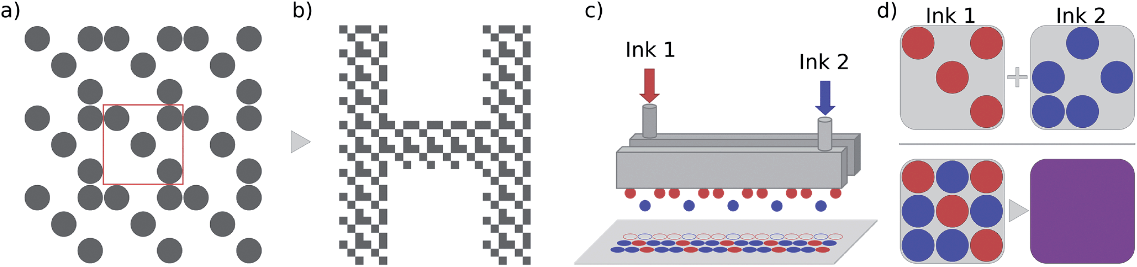 | ||
| Scheme 1 (a) A repetition of the base matrix with a 4/9 filling level used to control the amount of material deposited on the substrate by a single printhead. The central base matrix used in the algorithm described in the text is highlighted with a red square. (b) The 4/9 filling level base matrix from before, tiled in the shape of the letter “H”. (c) Schematic of the two printheads which are fed with two different inks that are simultaneously printed on the substrate. (d) Illustration of how the droplets of the two inks are placed on the substrate for a filling level of 4/9 for ink 1 and 5/9 for ink 2. The droplets of ink 2 are placed in the spaces left by ink 1 and can then intermix to form a homogeneous film of the desired composition. | ||
Once the base matrices for the different filling levels are created, the combinatorial inkjet printing of two inks is accomplished by printing the repetition of one base with ink 1 from the first printhead and simultaneously the inverse of this same base with ink 2 from the second printhead, see Scheme 1c. This means that ink 2 is printed in the spaces left blank by ink 1, see Scheme 1d. Assuming that the droplets are placed close enough together in space and time, the droplets can intermix to form the material with the desired ratio of the two inks. The distance between the droplets, or droplet pitch, is controlled by the resolution of the printing process, usually measured in “dots per inch” or dpi for short. For a resolution of 350 dpi in a given direction, the droplet pitch will be (2.54 × 104 μm per inch)/(350 dots per inch) ≈ 73 μm per dot. In comparison, the contact diameter of a 30 pl droplet printed on the substrate would be 103 μm, assuming a contact angle of 16°. The contact diameter is assumed to be the diameter of the circular footprint of the droplet on the substrate, see page 5 of the ESI† for details. In order for these droplets to come into contact with each other, the droplet pitch should not exceed 103 μm which is equivalent to a printing resolution of 248 dpi. In Scheme 2 the estimated droplet overlap is visualised for printing resolutions of 250, 350, and 450 dpi in both the x and the y directions, corresponding to droplet pitches of 102, 73, and 56 μm, respectively. In Scheme 2a, it can be seen that at 250 dpi the droplets just about touch the nearest neighbouring droplets and there is a rather large gap to neighbouring droplets on the diagonal. If the resolution is increased by a factor of  to 350 dpi the droplets also reach the neighbour on the diagonal, as is illustrated in Scheme 2b. If the resolution is further increased to 450 dpi the droplets start to overlap with multiple neighbours. At this resolution, the total amount of the precursor material deposited increases and the wet-film thickness will increase accordingly. This may lead to the deposited precursor material starting to flow outside the dedicated printing area. To avoid excessive spreading of the printed film as well as coffee ring formation we optimised the wetting of the printed film and used an immediate drying procedure of the wet film using vacuum and thermal annealing (see below).42 The dependence of the minimum printing resolution on the contact angle is shown in Fig. S4.†
 | ||
| Scheme 2 Illustration of droplet placement and overlap assuming a contact angle of 16° and a resulting droplet diameter of 103 μm for a printing resolution of (a) 250 dpi, (b) 350 dpi and (c) 450 dpi in both x and y directions. | ||
To validate the proposed combinatorial inkjet printing method the model system CsPb(BrxI1−x)3 was chosen. The resulting solid-solutions of CsPb(BrxI1−x)3 with x = 0 to 0.67 were investigated by preparing samples from two inks: ink 1 with a precursor composition of CsPbI3 (x = 0) and ink 2 with a precursor composition of CsPbBr2I (x = 0.67). The CsPbI3 precursor solution was prepared by dissolving 4 mmol of PbI2 (≥99.99% TCI) in 3 ml of dimethyl sulfoxide, DMSO, (≥99.9% Sigma Aldrich) and subsequently adding this solution to 4 mmol of CsI (≥99.999% ABCR). The second ink, CsPbBr2I (x = 0.67), was prepared by dissolving 4 mmol of PbBr2 (≥99.99% TCI) in 4 ml of DMSO and then adding this solution to 4 mmol of CsI (≥99.999% ABCR). Both inks were left to shake at 60 °C for 12 h. Before printing, 1 ml of dimethylformamide, DMF, (99.8% Sigma Aldrich) was added to the CsPbI3 ink to increase the evaporation rate and wetting on the substrate. The corresponding contact angle of the two inks on ozone cleaned quartz glass is shown in Fig. S5.†
To illustrate the possibility of deploying combinatorial inkjet printing in a custom geometry, the HySPRINT laboratory logotype with 9 filling levels from pure ink 2 (x = 0.67) on the left to pure ink 1 (x = 0) on the right was printed on photo paper (HP), see Fig. 1a. The two images used for this were generated by tiling the pixels of each character with a different 4 × 4 subpixel matrix (using every other base to get 9 filling levels) generated by the aforementioned algorithm. The bases used for the image for the first printhead were inverted to generate the image for the second printhead.
 | ||
| Fig. 1 (a) Logotype printed on paper with the different halide ratios of CsPb(BrxI1−x)3, from the left to the right. (b) Combinatorial library of CsPb(BrxI1−x)3 printed on quartz glass with ten samples from the top left to the bottom right labeled 1 to 10. (c) Optical bandgap of the ten samples from the combinatorial library in (b) determined from UV/vis transmission. | ||
For compositional and structural analysis, a set of combinatorial libraries were printed on quartz glass (GVB GmbH) by tiling all ten 3 × 3 base matrices in 8 × 8 mm2 squares. The squares were arranged in two rows of five with the top row from full, 9/9, filling of ink 1 (x = 0) to 5/9 filling from left to right followed by the second row with a filling of 4/9 to 0/9. The filling of ink 2 was once again realised by inverting the bases of the image for ink 1 and was therefore 9/9 in the bottom right corner and 0/9 in the top left. A set of combinatorial libraries were printed at 250, 350, and 450 dpi, respectively. Before printing, the substrates were ultrasonicated in Mucasol, water, acetone, and isopropanol, consecutively. Finally, the substrates were cleaned with a UV ozone treatment for 20 s immediately before printing. Printing was done in a nitrogen-filled glovebox on a PiXDRO LP50 printer with dual piezoelectrically activated drop-on-demand Spectra SE-128 printheads with a 30 pl drop-volume. To dry the printed wet film, the samples were all evacuated at ∼100 Pa for 450 s and annealed at 100 °C for 60 min after printing. Before measuring, the combinatorial libraries were placed on a 350 °C hotplate for 30 s to convert all samples to the orthorhombic Pbnm perovskite phase.
The combinatorial libraries were characterised by UV/vis transmittance measured using a custom-built mapping setup, photoluminescence (PL) through a microscope, confocal laser scanning microscopy (CFLSM) performed with a LEXT OLS4100, scanning electron microscopy (SEM), X-ray fluorescence (XRF) measured with a Bruker M4 Tornado and GIWAXS, performed at the μSpot beamline at BESSY II.43 The UV/vis transmittance was measured with white light illumination from a fibre-coupled halogen lamp, collected in an integrating sphere and measured by using a charge coupled device (CCD) spectrometer. The photoluminescence was excited by using a fibre-coupled 470 nm Thorlabs M470F3 LED driven at 1 A through a 40× objective and measured with a CCD spectrometer for 60 s per sample. CFLSM and SEM were both performed in the centre of each sample. The XRF was collected in vacuum (∼70 Pa) by excitation from a rhodium anode at a voltage of 50 kV and a current of 200 μA. GIWAXS was performed in a nitrogen-filled chamber with double Kapton windows at the μSpot beamline at BESSY II with a 9 keV beam cut down by a 10 μm pinhole and incident on the sample with an angle of 11.5° resulting in an illuminated area of 10 × 50 μm and a photon flux of 1014 cm−2 s−1. The diffracted beam was detected on an Eiger 9 M detector and integrated azimuthally using a LaB6 measurement as a reference.
Results
Fig. 1a shows an image of the result of our combinatorial printing method applied to the logo of the Helmholtz Innovation Laboratory HySPRINT. The shift in the optical bandgap from the high-bandgap CsPbBr2I precursor ink to pure CsPbI3 is visible by the naked eye and is due to the increase in lattice parameters as Br ions are being replaced by I ions in the lattice of the CsPb(BrxI1−x)3 solid solution. Fig. 1b shows an image of the 350 dpi combinatorial library of the same gradient printed in squares on a quartz substrate. The samples in the library are labeled 1 to 10 for future reference, with sample 1 being printed purely from the CsPbI3 ink and sample 10 being printed purely from the CsPbBr2I ink. Initially, the library was measured with UV/vis transmission spectroscopy and the optical bandgap (determined from the position of the maximum in the absolute value of the derivative of the transmittance) for each of the 10 samples given in Fig. 1b is shown in Fig. 1c. Additionally, the photoluminescence of the same samples was recorded and the spectra are shown together with the transmittance spectra in Fig. S6.† The optical bandgap is monotonically increasing with the Br content, as previously reported in the literature.44 However, the 1 mm spot size of the transmittance measurement averages over multiple droplets. The morphology of the films can be seen in the SEM pictures and CFLSM profiles in Fig. S10–S19† with the calculated RMS area roughness in Fig. S20† showing an average roughness below 60 nm.In order to investigate the compositional homogeneity of combinatorially printed samples on the length scale of the droplet pitch (73 μm for a resolution of 350 dpi), μ-spot GIWAXS and XRF mapping measurements with 50 μm resolution were conducted across a 1 mm × 1 mm spot in the centre of each sample. Fig. 2a shows a waterfall plot of the laterally averaged 110 and 220 peaks, for the orthorhombic Pbnm phase, of the azimuthally integrated GIWAXS patterns for each of the 10 samples in the combinatorial library. These peaks can be used to reliably determine the 110 lattice spacing accounting for any zero offset. The shift of the peak positions to higher q values when the Br content is increased is due to the reduction in lattice spacing as the larger I ions are gradually replaced by the smaller Br ions. The 110 lattice spacing derived from local GIWAXS measurements is plotted in a heat map in Fig. 2b.
 | ||
| Fig. 2 (a) Waterfall plot of the azimuthally integrated GIWAXS patterns in the range of the 110 and 220 peaks. The patterns are an average of all spots mapped within each sample in the combinatorial library shown in Fig. 1b. (b) Heatmap of the 110 lattice spacing mapped with 50 μm resolution in the centre of each of the samples. (c) Averaged XRF spectra of all the samples with the background subtracted and normalised by the Pb L3-M5 line. (d) Heatmap of the Br content mapped with 50 μm resolution in the centre of each of the samples, assuming an average value of x = 0.67 for sample 10. | ||
Similarly, the laterally averaged XRF spectra for each sample in the range of the I, Cs and Pb L-lines as well as the Br K-lines are plotted in Fig. 2c. All XRF spectra were background subtracted and normalised by the Pb L3-M5 line to decouple any thickness variations. The spectra show a reduction in the I L3-M5 transition to 1/3rd of the peak area as iodide is replaced by bromide. On the other hand, the Br K-L3 peak increases from zero with a linear increase in area, whilst the Cs L2-M4 peak remains constant. The Br content, x, in the CsPb(BrxI1−x)3 solid solution can be calculated from the XRF map using the area of the Br K-L3 peak, assuming that sample 10 has an average value of x = 0.67. The calculated Br content, x, is plotted in a heat map in Fig. 2d.
The heat maps of GIWAXS and XRF data show distinct distributions for each sample with only small variations from the intended composition. From the small variations there is a clear correlation between the lattice spacing and composition in the CsPb(BrxI1−x)3 samples. To quantify the compositional distributions derived from GIWAXS and XRD, respectively, a correlation plot of lattice spacing vs. the Br content with histograms for the two measurements is shown in Fig. 3. The correlation plot shows that there is a close to linear dependence of the 110 lattice spacing on the Br content in the solid solution with a slight bowing in agreement with the literature.44 This correlation implies that the 110 lattice spacing can be used to determine the Br content and thereby the intermixing of the two inks. Additionally, the histograms show that we have more narrow distributions from the GIWAXS measurements, most likely due to less noise when determining a peak position for the GIWAXS rather than a peak area in the case of XRF. In general, the histograms for the samples around 50![[thin space (1/6-em)]](https://www.rsc.org/images/entities/char_2009.gif) :50 mixing of the two inks indicate a broader compositional distribution for both measurements. The endpoints for the lattice spacing distributions, corresponding to the pure inks, are the sharpest and show that the real experimental uncertainty is much lower than that for the highest Br content XRF distribution. The distribution of the XRF values for the pure iodide sample is noticeably sharper due to the lack of a Br peak and any variation from zero is noise in the background.
:50 mixing of the two inks indicate a broader compositional distribution for both measurements. The endpoints for the lattice spacing distributions, corresponding to the pure inks, are the sharpest and show that the real experimental uncertainty is much lower than that for the highest Br content XRF distribution. The distribution of the XRF values for the pure iodide sample is noticeably sharper due to the lack of a Br peak and any variation from zero is noise in the background.
 | ||
| Fig. 3 Mean 110 lattice spacing as a function of the mean Br content determined from GIWAXS and XRF, respectively. Error bars represents ±1 standard deviation of the mean. Histograms of all measured spots for the 10 samples are shown on top for the Br content from XRF and to the right for 110 lattice spacing from GIWAXS. | ||
To investigate the effect of the printing resolution, which results in a varying distance between the deposited droplets on the substrate and therefore also in the amount of material deposited, the GIWAXS mapping was performed on two additional libraries printed with a resolution of 250 and 450 dpi, respectively. The calculated 110 lattice spacing as a function of its position is shown in Fig. 4 together with the printed image for three out of the ten samples for each of the libraries printed at 250, 350, and 450 dpi. The samples with 3/9, 5/9, and 7/9 filling of the CsPbBr2I ink were chosen as Fig. 3 shows that the largest inhomogeneity occurs for the samples with lattice parameters between 595 and 610 pm, corresponding to fillings from 3/9 to 7/9. The histograms of the calculated 110 lattice spacing for all the samples of the three libraries are shown in Fig. S7–S9.†
 | ||
| Fig. 4 (a)–(c), (g)–(i) and (m)–(o) The centre mm2 of the images sent to the printheads for filling levels 3/9, 5/9 and 7/9 of the CsPbBr2I ink for printing resolutions of 250, 350 and 450 dpi corresponding to droplet pitches of 102, 73 and 56 μm, respectively. Yellow is for the printhead with CsPbI3 and dark blue is for the printhead with CsPbBr2I. (d)–(f), (j)–(l) and (p)–(r) Heatmaps of the 110 lattice spacing for the corresponding printed image calculated from the μ-spot GIWAXS mapping. | ||
From the heatmaps of the lattice spacing in Fig. 4 we can see that there is local inhomogeneity on the scale of the printed image for the large drop distance at 250 dpi, as can be seen by comparing Fig. 4a and d. Additionally, there are holes in the film shown as white squares in Fig. 4p. This is also reflected in the other samples as can be seen by the broad overlapping distributions in the histogram in Fig. S7.† When the distance between the droplets is reduced to 73 μm, as we increase the resolution to 350 dpi, the samples are much more homogeneous and a continuous film is formed as can be seen in Fig. 4e, k and q. This holds true for the rest of the samples which is evident from the narrow distributions in Fig. 3. However, if even more material is placed on the sample, as is the case for the library printed at 450 dpi, inhomogeneity on a length scale larger than that of the printed image can be observed. This large-scale inhomogeneity is apparent in a deviation from the targeted composition in Fig. 4f and as features larger than the printed image when comparing Fig. 4i and l. This is once again visible in the histogram in Fig. S9† where the distributions are still sharp but the positions are no longer linearly spaced as intended. The morphology of the corresponding samples can be seen in the SEM pictures in Fig. S21† and is less dependent on the printing resolution and more on the substrate-ink compatibility.
Discussion
The analysis shows that synchrotron-based μ-spot GIWAXS is uniquely suited for characterising the homogeneity of the chosen material system as it can be mapped with a spot size smaller than the distances between printed droplets and more importantly shows a long-range order, and therefore mixing, on an atomic scale. Additionally, μ-spot GIWAXS provides excellent resolution for the halide ratio in our solid solution as the information is extracted from a signal peak shift rather than a small change in intensity.With this method, we demonstrate that the algorithm for droplet placement provides thin films with intermixing on the nanometer scale, when the printing resolution allows effective intermixing of the co-deposited precursor inks. Furthermore, it can be seen that optimised deposition parameters enable the synthesis of films with the intended composition on the ∼100 μm length scale of our printing resolution. The mean standard deviation of the 110 lattice spacing for the samples in the library printed at 350 dpi is only 0.5 pm. This corresponds to a Gaussian broadening of the optical bandgap by a FWHM of only 18 meV which is smaller than kBT = 26 meV at room temperature.
When the printing resolution is too low (see the 250 dpi case shown in Fig. 4) the droplet pitch is too high compared with the droplet diameter on the substrate. In this case, there is limited contact between the droplets, which means that the time is too short for the precursor inks to intermix effectively before the film dries and the precursors are converted to solid state phases. On the other hand, if too much material is deposited on the substrate, which is the case for the films printed with 450 dpi, the substantially thicker wet film enables long-range inter-diffusion of the deposited material prior to the drying process. This leads to demixing on a large scale (mm) as evidenced by the deviation from the intended composition in Fig. 4f. Such a deviation from the intended composition has previously been reported in the literature for mixed halide inorganic perovskites.45 Nevertheless, by varying the resolution and, thereby, the distance between the droplets and the amount of ink, an optimal deposition window can be accessed where these problems are overcome.
Suitable printing parameters can be found by calculating the minimum resolution needed for the droplets to be in contact with each other. Assuming a drop volume of 30 pl and a contact angle of 16° the droplet contact diameter would be 103 μm and the minimum resolution would be 248 dpi. This is the resolution at which adjacent droplets start to be in contact, and corresponds to the printing conditions shown in Fig. 4d. From the noticeable inhomogeneities and correlation of spatial distribution of lattice parameters with the droplet pattern, it can be concluded that the corresponding droplet pitch is not sufficient to ensure complete intermixing of the droplets.
In order for an individual droplet to connect with all the surrounding droplets, including those on the diagonal, the resolution has to increase by a factor of  to 342 dpi, corresponding to the printing parameters of the samples displayed in Fig. 4e, k, and q. For these printing parameters, good homogeneity is observed as evidenced by the heatmaps of the 110 lattice spacing. If the droplet pitch is decreased significantly below this value, the wet film cannot be contained within its original area and will flow out on the substrate, and facilitates macroscopic diffusion leading also to possible phase segregation (Fig. 4l). To avoid this effect, a printhead with a smaller drop volume would have to be used. With a smaller drop volume, the resolution can be increased to improve the intermixing without increasing the amount of ink deposited.
We have previously shown how this combinatorial ink-jet printing method can be applied to generate samples facilitating the fast determination of the phase diagram of a complete solid solution of CsPb(IxBr1−x)3.41 We believe that the possible applications of combinatorial inkjet printing go far beyond that. Although the current study was focused on a crystalline semiconductor, the approach can be applied to any miscible inks with similar rheological properties. Additionally, the method is not limited to two inks but can easily be adapted to any number of inks and printheads to directly fabricate devices with tuneable and laterally structured semiconductors, as shown elsewhere.25
Conclusions
In conclusion, we have presented a successful algorithm for the generation of print patterns with optimised drop placement for combinatorial inkjet printing. This algorithm allows variation of the number of droplets printed for each ink throughout the sample. With this method, we were able to print a custom image with 10 different halide compositions of CsPb(BrxI1−x)3. The homogeneity of combinatorial libraries of CsPb(BrxI1−x)3 was determined using synchrotron-based GIWAXS mapping with a μ-spot and lab-based XRF mapping. We have shown that for too low printing resolutions the material does not intermix completely and that for too high resolution the thick wet film causes large-scale demixing. However, if the resolution is optimised the method produces homogeneous films with intermixing on the atomic scale, thus providing a powerful method for high-throughput investigation of solution-processed thin film materials.Author contributions
Contributions according to the CRediT standardised contribution descriptions: conceptualisation: EU (lead), HN (lead), ELK (supporting), and TU (supporting); data curation: OS (equal) and IZ (equal); formal analysis: HN (lead) and PB (supporting); funding acquisition: EU; investigation: HN (lead) and OS (supporting); methodology: HN; project administration: HN; resources: EU (equal), IZ (equal), PB (equal), TU (equal), OS (equal), ELK (supporting), and FM (supporting); software: HN; supervision: TU and EU; validation: VS; visualisation: HN; writing – original draft: HN; writing – review & editing: all co-authors.Conflicts of interest
There are no conflicts to declare.Acknowledgements
HN, OS, FM, and EU acknowledge funding from the German Ministry of Education and Research (BMBF) for the Young Investigator Group Hybrid Materials Formation and Scaling (HyPerFORME) within the program “NanoMatFutur”(grant no. 03XP0091). OS and EU acknowledge funding from the German Science Foundation (DFG) provided in the framework of the priority program SPP 2196, “Perovskite semiconductors: from fundamental properties to devices” Project number 424394788. HN, PB, and TU acknowledge the support from the HyPerCells graduate school and HN thanks the HI-SCORE research school. This work was carried out in the framework of the Joint Lab GEN_FAB and with the support of the Helmholtz Innovation Lab HySPRINT. The authors would like to thank Carola Klimm for the SEM measurements and the BESSY II synchrotron in Berlin for use of beamtime at the mySpot beamline.Notes and references
-
A. Aspuru-Guzik and K. Persson, Materials Acceleration Platform: Accelerating Advanced Energy Materials Discovery by Integrating High-Throughput Methods and Artificial Intelligence, Mission Innovation: Innovation Challenge, 2018, vol. 6 Search PubMed
.
- T. J. Jacobsson, J.-P. Correa-Baena, M. Pazoki, M. Saliba, K. Schenk, M. Grätzel and A. Hagfeldt, Energy Environ. Sci., 2016, 9, 1706 RSC
- W. F. Maier, ACS Comb. Sci., 2019, 21, 437–444 CrossRef CAS PubMed
- J. G. Tait, S. Manghooli, W. Qiu, L. Rakocevic, L. Kootstra, M. Jaysankar, C. A. Masse De La Huerta, U. W. Paetzold, R. Gehlhaar, D. Cheyns, P. Heremans and J. Poortmans, J. Mater. Chem. A, 2016, 4, 3792–3797 RSC
- D. Maclean, J. J. Baldwin, V. T. Ivanov, Y. Kato, A. Shaw, P. Schneider, E. M. Gordon, S. Campbell, K. Chapman, V. Ivanov and S. Rao, Pure Appl. Chem., 1999, 71, 2349–2365 CAS
- P. J. McGinn, ACS Comb. Sci., 2019, 21, 501–515 CrossRef CAS PubMed
- S. O. Klemm, A. G. Martin, J. Lengsfeld, J.-C. Schauer, B. Schuhmacher and A. W. Hassel, Phys. Status Solidi, 2010, 207, 801–806 CrossRef CAS
- S. Guerin and B. E. Hayden, J. Comb. Chem., 2006, 8, 66–73 CrossRef CAS PubMed
- K. Kennedy, T. Stefansky, G. Davy, V. F. Zackay and E. R. Parker, J. Appl. Phys., 1965, 36, 3808–3810 CrossRef CAS
- A. Teichler, R. Eckardt, S. Hoeppener, C. Friebe, J. Perelaer, A. Senes, M. Morana, C. J. Brabec and U. S. Schubert, Adv. Energy Mater., 2011, 1, 105–114 CrossRef CAS
- A. Queraltó, J. Banchewski, A. Pacheco, K. Gupta, L. Saltarelli, D. Garcia, N. Alcalde, C. Mocuta, S. Ricart, F. Pino, X. Obradors and T. Puig, ACS Appl. Mater. Interfaces, 2021, 13, 9101–9112 CrossRef PubMed
- M. Bag, Z. Jiang, L. A. Renna, S. P. Jeong, V. M. Rotello and D. Venkataraman, Mater. Lett., 2016, 164, 472–475 CrossRef CAS
- A. C. Arias, J. D. MacKenzie, I. McCulloch, J. Rivnay and A. Salleo, Chem. Rev., 2010, 110, 3–24 CrossRef CAS PubMed
- D. MacKenzie, J. Breeden, J. Chen, P. Hinkle, E. Jones, A. Menon, Y. Nakazawa, J.-H. Shin, V. Vo, M. Wilkinson, Y. Yoshioka and J. Zhang, SID Int. Symp. Dig. Tech. Pap., 2009, 40, 20 CrossRef
- C. F. Du, Q. Liang, Y. Luo, Y. Zheng and Q. Yan, J. Mater. Chem. A, 2017, 5, 22442–22458 RSC
- K. H. Choi, J. T. Yoo, C. K. Lee and S. Y. Lee, Energy Environ. Sci., 2016, 9, 2812–2821 RSC
- M. A. Green, E. D. Dunlop, J. Hohl-Ebinger, M. Yoshita, N. Kopidakis and X. Hao, Prog. Photovoltaics Res. Appl., 2021, 29, 657–667 CrossRef
- NREL, Best Research-Cell Efficiency Chart 2021, accessed 4 July 2021, https://www.nrel.gov/pv/cell-efficiency.html.
- J. Peng, D. Walter, Y. Ren, M. Tebyetekerwa, Y. Wu, T. Duong, Q. Lin, J. Li, T. Lu, M. A. Mahmud, O. L. C. Lem, S. Zhao, W. Liu, Y. Liu, H. Shen, L. Li, F. Kremer, H. T. Nguyen, D. Y. Choi, K. J. Weber, K. R. Catchpole and T. P. White, Science, 2021, 371, 390–395 CrossRef CAS PubMed
- Z. K. Tan, R. S. Moghaddam, M. L. Lai, P. Docampo, R. Higler, F. Deschler, M. Price, A. Sadhanala, L. M. Pazos, D. Credgington, F. Hanusch, T. Bein, H. J. Snaith and R. H. Friend, Nat. Nanotechnol., 2014, 9, 687–692 CrossRef CAS PubMed
- F. Hermerschmidt, F. Mathies, V. R. F. Schröder, C. Rehermann, N. Z. Morales, E. L. Unger and E. J. W. List-Kratochvil, Mater. Horiz., 2020, 7, 1773–1781 RSC
- H. Wei, Y. Fang, P. Mulligan, W. Chuirazzi, H. H. Fang, C. Wang, B. R. Ecker, Y. Gao, M. A. Loi, L. Cao and J. Huang, Nat. Photonics, 2016, 10, 333–339 CrossRef CAS
- L. Basiricò, A. Ciavatti and B. Fraboni, Adv. Mater. Technol., 2021, 6, 2000475 CrossRef
- L. Dou, Y. M. Yang, J. You, Z. Hong, W. H. Chang, G. Li and Y. Yang, Nat. Commun., 2014, 5, 1–6 Search PubMed
- V. R. F. Schröder, F. Hermerschmidt, S. Helper, C. Rehermann, G. Ligorio, H. Näsström, E. L. Unger and E. J. W. List-Kratochvil, Adv. Eng. Mater., 2021, 2101111 CrossRef
- T. Todorov, O. Gunawan and S. Guha, Mol. Syst. Des. Eng., 2016, 1, 370–376 RSC
- A. Al-Ashouri, E. Köhnen, B. Li, A. Magomedov, H. Hempel, P. Caprioglio, J. A. Márquez, A. B. M. Vilches, E. Kasparavicius, J. A. Smith, N. Phung, D. Menzel, M. Grischek, L. Kegelmann, D. Skroblin, C. Gollwitzer, T. Malinauskas, M. Jošt, G. Matič, B. Rech, R. Schlatmann, M. Topič, L. Korte, A. Abate, B. Stannowski, D. Neher, M. Stolterfoht, T. Unold, V. Getautis and S. Albrecht, Science, 2020, 370, 1300–1309 CrossRef CAS PubMed
- F. Lang, O. Shargaieva, V. V. Brus, H. C. Neitzert, J. Rappich and N. H. Nickel, Adv. Mater., 2018, 30, 1702905 CrossRef PubMed
- M. Saliba, T. Matsui, J. Y. Seo, K. Domanski, J. P. Correa-Baena, M. K. Nazeeruddin, S. M. Zakeeruddin, W. Tress, A. Abate, A. Hagfeldt and M. Grätzel, Energy Environ. Sci., 2016, 9, 1989–1997 RSC
-
E. L. Unger, O. Shargaieva, S. Braunger and P. Docampo, in Solar
Energy Capture Materials, ed. E. A. Gibson, Royal Society of Chemistry, Cambridge, 2019, pp. 153–192 Search PubMed
- P. Prajongtat, C. Sriprachuabwong, R. Wongkanya, D. Dechtrirat, J. Sudchanham, N. Srisamran, W. Sangthong, P. Chuysinuan, A. Tuantranont, S. Hannongbua and N. Chattham, ACS Appl. Mater. Interfaces, 2019, 11, 27677–27685 CrossRef CAS PubMed
- S. G. Li, K. J. Jiang, M. J. Su, X. P. Cui, J. H. Huang, Q. Q. Zhang, X. Q. Zhou, L. M. Yang and Y. L. Song, J. Mater. Chem. A, 2015, 3, 9092–9097 RSC
- S. G. Hashmi, D. Martineau, X. Li, M. Ozkan, A. Tiihonen, M. I. Dar, T. Sarikka, S. M. Zakeeruddin, J. Paltakari, P. D. Lund and M. Grätzel, Adv. Mater. Technol., 2017, 2, 1600183 CrossRef
- C. Liang, P. Li, H. Gu, Y. Zhang, F. Li, Y. Song, G. Shao, N. Mathews and G. Xing, Sol. RRL, 2018, 2, 1700217 CrossRef
- H. Eggers, F. Schackmar, T. Abzieher, Q. Sun, U. Lemmer, Y. Vaynzof, B. S. Richards, G. Hernandez-Sosa and U. W. Paetzold, Adv. Energy Mater., 2020, 10, 1903184 CrossRef CAS
- A. Gheno, Y. Huang, J. Bouclé, B. Ratier, A. Rolland, J. Even and S. Vedraine, Sol. RRL, 2018, 2, 1800191 CrossRef
- Z. Li, P. Li, G. Chen, Y. Cheng, X. Pi, X. Yu, D. Yang, L. Han, Y. Zhang and Y. Song, ACS Appl. Mater. Interfaces, 2020, 12, 39082–39091 CrossRef CAS PubMed
- P. Li, C. Liang, B. Bao, Y. Li, X. Hu, Y. Wang, Y. Zhang, F. Li, G. Shao and Y. Song, Nano Energy, 2018, 46, 203–211 CrossRef CAS
- S. Chen, L. Zhang, L. Yan, X. Xiang, X. Zhao, S. Yang and B. Xu, Adv. Funct. Mater., 2019, 29, 1905487 CrossRef CAS
- S. Chen, L. Zhang, Y. Liu, Z. Zhang, Y. Li, W. Cai, H. Lv, Y. Qin, Q. Liao, B. Zhou, T. Yan, J. Ren, S. Chen, X. Xiang, S. Dai, S. K. So, X. Wang, S. Yang and B. Xu, J. Mater. Chem. A, 2021, 9, 25502–25512 RSC
- H. Näsström, P. Becker, J. A. Márquez, O. Shargaieva, R. Mainz, E. Unger and T. Unold, J. Mater. Chem. A, 2020, 8, 22626–22631 RSC
- F. Mathies, E. R. Nandayapa, G. Paramasivam, M. F. Al Rayes, V. R. F. Schröder, C. Rehermann, E. J. W. List-Kratochvil and E. L. Unger, Mater. Adv., 2021, 2, 5365–5370 RSC
- I. Zizak, J. large-scale Res. Facil., 2016, 2, 101 CrossRef
- R. E. Beal, D. J. Slotcavage, T. Leijtens, A. R. Bowring, R. A. Belisle, W. H. Nguyen, G. F. Burkhard, E. T. Hoke and M. D. Mcgehee, J. Phys. Chem. Lett., 2016, 7, 746–751 CrossRef CAS PubMed
- H. Funk, O. Shargaieva, A. Eljarrat, E. L. Unger, C. T. Koch and D. Abou-Ras, J. Phys. Chem. Lett., 2020, 11, 4945–4950 CrossRef CAS PubMed
Footnote |
| † Electronic supplementary information (ESI) available. See DOI: 10.1039/d1ta08841f |
| This journal is © The Royal Society of Chemistry 2022 |