
 Open Access Article
 This Open Access Article is licensed under a Creative Commons Attribution-Non Commercial 3.0 Unported Licence
Progress and challenges on scaling up of perovskite solar cell technology
Jin
Yan
 a,
Tom J.
Savenije
b,
Luana
Mazzarella
a and
Olindo
Isabella
*a
a,
Tom J.
Savenije
b,
Luana
Mazzarella
a and
Olindo
Isabella
*a
aPhotovoltaic Materials and Devices, Delft University of Technology, Mekelweg 4, 2628 CD Delft, The Netherlands. E-mail: O.Isabella@tudelft.nl
bDepartment of Chemical Engineering, Delft University of Technology, van der Maasweg 9, 2629 HZ Delft, The Netherlands
First published on 1st December 2021
Abstract
Since the first application of a metal halide perovskite (PVK) absorber in a solar cell, these materials have drawn a great deal of attention in the photovoltaic (PV) community, showing exceptional rapid progress in power conversion efficiency. The potential advantages of low-cost, high efficiency, easy processability, and wide range of applications make PVK solar cells (PSCs) a desirable candidate for future uptake in the PV market over traditional semiconductors such as silicon. Furthermore, PVK thin-film technology holds a concrete potential to closely approach the theoretical efficiency limit for single-junction solar cells via unique control of the optoelectronic properties. However, for a disruptive breakthrough of PVK technology from fundamental research to industry, systematic research efforts are required to unravel the poor long-term stability and to reach a reliable large area fabrication process. In this review, we examine in detail recent progress on large-scale PSCs and we discuss challenges for commercialization touching upon the following aspects: material properties, fabrication technology, and industrialization challenges. Besides, the long-term stability and efficiency of large-area PSCs as well as PVK-based two-terminal tandem devices are discussed. In addition, strategies for PSC upscaling are further studied for scalable deposition technologies. Finally, we review the most recent literature on costs and environmental assessment.
1. Introduction
Photovoltaic (PV) technology converts solar energy into electricity. Over the last seventy years, many different absorber materials and device architectures have been developed resulting in high power conversion efficiencies (PCEs). Among them, crystalline silicon (c-Si) and so-called III–V solar cells have demonstrated high efficiencies and a mature level of development. Currently, c-Si solar cells dominate more than 90% of the PV market share1 because of cheap raw materials, long stability, and well-established technology. However, the limitation of c-Si PV is the complex fabrication process as well as high requirements for wafer quality, which increase the fabrication cost and hinder further commercialization of high-efficiency architectures.2–4 The promise of emerging thin-film PV technology is to cost-effectively fabricate high-quality semiconductor materials by simpler deposition processes and reducing the amount of material used.Over the last decade, organic–inorganic metal halide perovskite (PVK) has attracted much attention in the PV research community, after Kojima et al.5 discovered in 2009 the ability of PVK to convert the energy carried by sunlight into electricity. The reasons behind the success of PVK can be ascribed to its exceptional electrical properties with direct bandgap and high absorption coefficient, long carrier diffusion length, tuneable bandgap by compositional engineering, and simplified deposition process. With these outstanding properties, PVK solar cells (PSCs) have been developed rapidly, demonstrating in only a decade, albeit on a sensibly smaller device area, PCEs approaching those recorded by solar cells based on c-Si.6
However, compared to c-Si, PVK technology still has two main drawbacks namely device stability and device upscaling. These two factors directly determine the steps toward commercialization. Pinholes and defects existing in thin films have a negative impact on photoelectric properties7,8 and their influence becomes more severe for an effective lab-to-fab transition.9 To address this problem, various scalable deposition strategies are employed for each layer of the PSC to obtain high-quality films and excellent device properties. Challenges in device stability, as well as cost including environmental impact, are all crucial topics of relevance for the PV industry.
In fact, PVKs suffer from different degradation pathways related to temperature,10,11 humidity,12,13 composition,14 and light.15,16 This leads to decomposition of the material and decrease of performance as time goes on. Several approaches17–20 have been explored to prevent this reduction in performance. Recently, PVK degradation mechanisms have been reported21 and different materials are tested to replace less stable systems.22 Up to now, large-scale (100 cm2) PSCs show promising stabilities.23,24 Nevertheless, there is still a long way towards commercialization, especially compared with c-Si PV. An approach to control degradation deals with tailoring the nature of the PVK lattice by using various cations25 and halide anions.26,27 Other strategies comprise functionalizing the PVK material to improve stability.28
Although there are numerous challenges, the progress of PSCs towards commercialization is unprecedented in the PV community. Many technologies are demonstrated to be suitable for scalable film deposition, which can produce each layer of PSC with high film quality. With the application of various strategies, such as precursor engineering and interfacial engineering, the efficiency for large area devices has been largely improved. PSCs with an active area of more than 57 cm2 have been fabricated with a certified PCE of 14.6%.29
Besides, PVK is also employed as at least one of the absorbers in double and triple-junction solar cells fully based on PVK PV technology30–32 or in combination with c-Si PV technology. For their promising PCEs, the PVK-based tandem solar cells provide a valuable economic approach to break through the Shockley and Queisser (SQ) limit33 for single-junction devices. Currently, the world record PCE for PVK/c-Si tandem solar cell has achieved 29.8%.34 Apart from efficiency, long-term stability has also been improved in the last years with the introduction of inorganic cations, such as cesium (Cs). Nowadays, large-area devices are reported to work consistently for 1000 h under the condition of 25 °C and 85% humidity with an area of 25 cm2.35 With further development of encapsulation technology and device optimization, the device stability aims at fulfilling the test requirements for commercialization in near future.
In this review, we discuss recent progress in large-scale PSCs and focus on the challenges for commercialization. Section 2 summarizes several high-volume manufacturing technologies which are suitable for scalable deposition of PVK film. Section 3 summarizes the challenges of up-scaling for different PVK layers. Section 4 provides an overview of efficiency and stability for large area PVK-based monolithic tandem solar cells. Additionally, to have a reasonable assessment of PVK industrialization, cost and environmental impact are discussed in Section 5. Finally, we review several companies which have started their business using PSCs for a variety of applications.
2. Progress for scalable techniques
Fabrication of uniform and pinhole-free large-area PVK films can be realized by employing suitable deposition methods, such as blading, slot die coating, spray deposition and more. In this section, we review some deposition methods enabling scalable processes for PVK film fabrication.2.1 Solution based processes
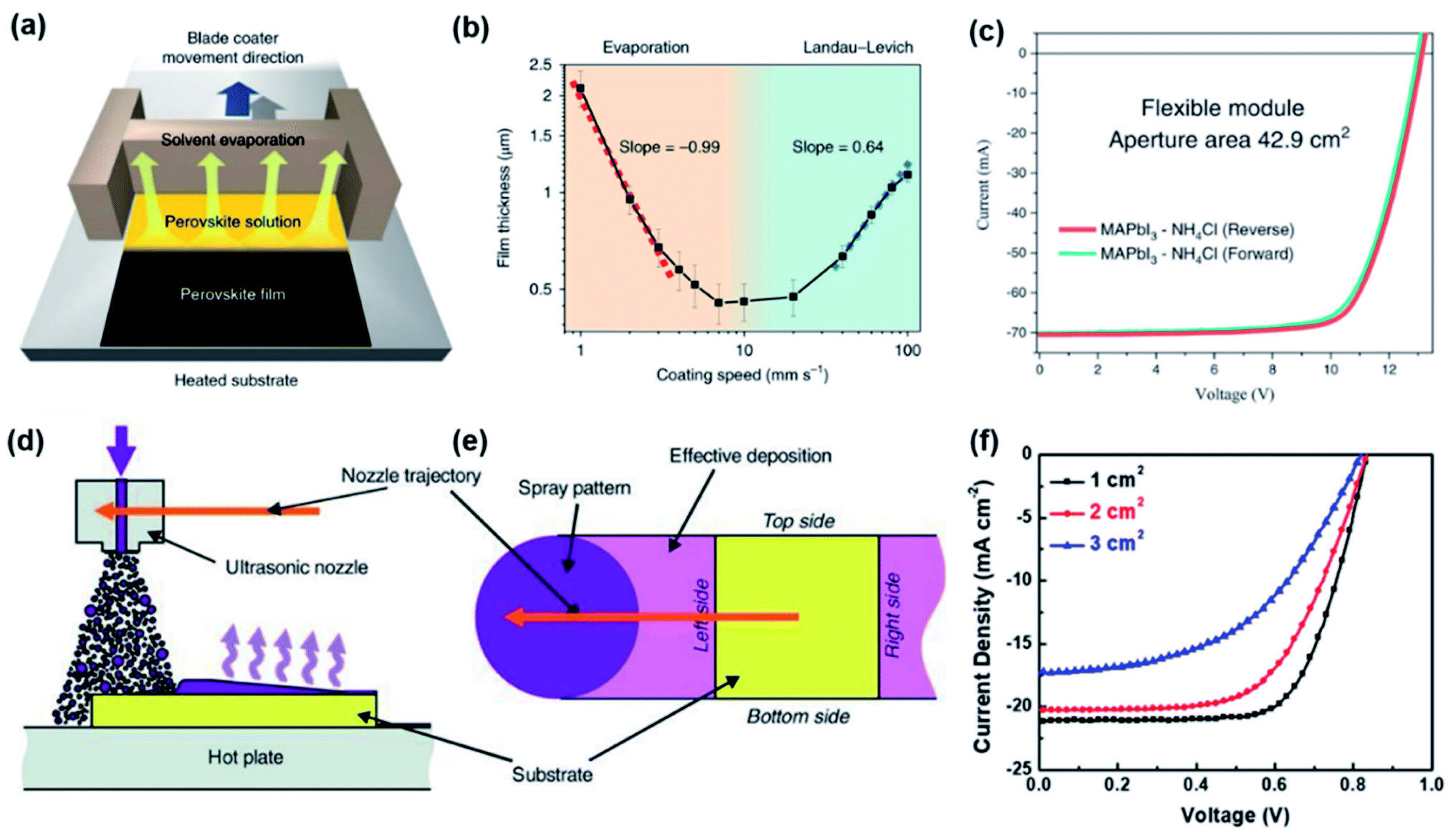 | ||
| Fig. 1 (a) Diagram of blade coating of PVK film29 (b) the film thickness as a function of coating speed for blade coating29 (c) J–V curves for flexible PSCs with a record aperture area of 42.9 cm2 and PCE of 15.86% (ref. 36) (d) diagram of the spray coating process49 (e) diagram of the magnified structure of nozzle trajectory49 (f) J–V curves for PSCs with different active areas.50 | ||
2.2 Vacuum based processes
As an alternative to solution-based processes, vacuum deposition has been explored to grow thin-film PVK from dry sources. There are two unique advantages of vacuum-based process. Firstly, the process does not involve the use of toxic solvents which may have a negative effect on the environment. The second advantage is the conformal growth onto rough substrates allowing, for example, the use of textured substrates in devices to improve light in-coupling.84 This opens the integration of PVK cells on textured c-Si bottom cells for further applications.85–87
 | ||
| Fig. 4 (a) Schematic diagram of the PLD configuration and deposition process103 (b) top view of PVK film on silicon wafer deposited with PLD103 (c) the cross-section of the PLD PVK film103 (d) schematic diagram of the HCVD configuration for MAI deposition onto PbI2 coated substrates109 (e) image of cells and modules prepared with HCVD approach demonstrating the up-scaling process.110 | ||
2.3 Hybrid chemical vapor deposition
Hybrid chemical vapour deposition (HCVD) method can avoid solvent-related complications, which are challenging to control in industrial large-scale fabrication,111 such as fast solvent removal and wettability issues. This method combines chemical vapour deposition (CVD) and other scalable deposition methods, such as thermal evaporation112 or spray coating.113 A typical PVK-based HCVD process consists of two steps: formation of inorganic film and organic/inorganic halide vapour deposition. The inorganic film is mainly deposited via thermal evaporation in reported works.213,216 As for the CVD process, the organic halide vapour is optimized by pressure and temperature to deposit on the inorganic film, following a gas–solid reaction and converting into uniform PVK films.114 The HCVD configuration and vapour deposition process for MAPbI3 are shown in Fig. 4d. Several works have reported a successful formation of scalable PVK films by combining thermal evaporation and CVD.109,110,115 Leyden et al.109 firstly prepared a planar MAPbCl3 device via HCVD method, achieving a PCE as high as 11.8%. Following the similar approach, Leyden et al.110 again indicated the device upscaling process via HCVD. They fabricated MAPbI3 based devices with a PCE of 9.5% (8.8 cm2) and obtained a PCE of 9.0% (12 cm2) for FAPbI3 based devices, the corresponding up-scaling processes are shown in Fig. 4e. However, similarly to solution-based film formation, mixed-cations and mixed-halides play a critical role in film optoelectronic properties and stability.115 Therefore, mixed cations/halides are commonly introduced in the first step by co-evaporation.116 Differently from this approach, Luo et al.112 prepared a mixed-cation PVK film by optimizing the second step. They replaced pure FAI vapour with FAI/FACl mixed vapour to optimize the vapour–solid reaction, resulting in improved phase stability. Consequently, the large-sized PSC modules (active area of 41.25 cm2) demonstrated champion PCE of 12.24%.3. Challenges for device upscaling
The abovementioned deposition techniques are all for large area PVK film formation. As for other methods (e.g. CVD, soft-cover deposition), detailed technical parameters and models can be found somewhere else.113,116–118 The device PCEs, deposition approaches, and corresponding areas are summarized in Fig. 5, which clearly shows that PCEs significantly decrease for large device areas. Therefore, the upscaling of PVK PV technology still faces challenges toward commercialization. In this section, we review the most significant challenges for processing high PCE devices from lab-scale to fab-scale.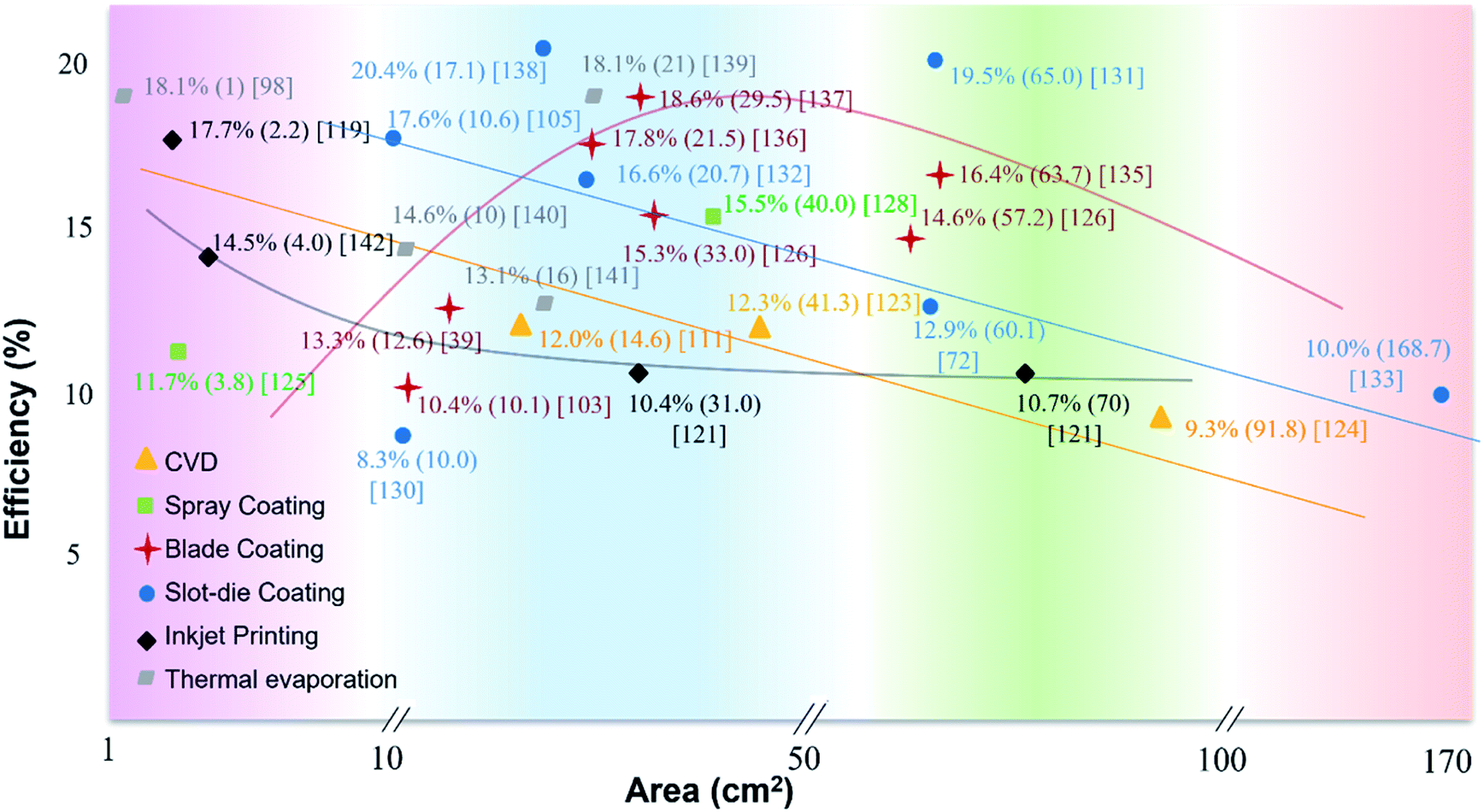 | ||
| Fig. 5 Summary of PCEs as a function of the device area for PSCs prepared by different fabrication methods.39,57,72,80,83,98,111,113,119–122,122–142 | ||
3.1 Precursors and absorber layer
Upscaling of PVK films emphasizes the suitable storage of precursors as well as film deposition process. For solution-based methods, the precursor solution ratio and storage may have impacts on film quality, influencing both the nucleation and the crystal growth. To address this question, many attempts have been performed to control the film morphology and photovoltaic performance starting from a non-stoichiometric precursor solution.143,144 As an example, excess of PbI2 can lead to higher PCEs suggesting that unreacted PbI2 improves the crystallinity of PVK films.145 The reported precursor engineering may have some differences based on different solution deposition methods, but most of them are related to introducing of additives as stabilizer or mixing solvents to optimize the precursor viscosity as well as boiling point.146Table 1 briefly shows the reported requirements, approaches and corresponding solution-based deposition methods. Besides, the detailed PVK precursor solution chemistry is reviewed by Jung et al.147 from fundamentals to industrialization.| Methods | Requirements | Approaches |
|---|---|---|
| Blade coating | Purified organic precursor148 | Reductant149,150 |
| High viscosity39 | Moisture barrier151 | |
| Material with synergistic effects152 | ||
| Spray coating | Low viscosity147 | Co-solvents153 |
| Suitable boiling point solvent51 | Low ink concentrations54,154 | |
| Material with synergistic effects155 | ||
| Slot die coating | — | Co-solvents156–158 |
| Lewis base additive71 | ||
| Material with synergistic effects134,159,160 | ||
| Inkjet printing | Slow solvent evaporation161 | Material with synergistic effects82,162–164 |
| Co-solvents165 |
Compared with solution-based methods, vacuum deposition can exactly control the deposited amount. However, one of the drawbacks is the lack of compatibility with additive engineering, which is an excellent approach to improve crystal quality, as shown in Table 2. Furthermore, this method shows less flexibility in the number of sources that can be incorporated in the final PVK material. For the deposition process, one of the most challenging part is to form a suitable interaction between substrate and precursors for both solution and vacuum related deposition approaches.166 A better interaction not only depresses formation of non-radiative centres in the interfacial, but also has an influence on PVK crystal growth.
| Advantages | Disadvantages | |
|---|---|---|
| Solution methods | • Simple | • Solvent usage168 |
| • Compatible with additive engineering167 | • Low material utilization169 | |
| Vacuum methods | • Uniformity control on large area | • limitation in number of sources evaporated |
| • Non-toxic solvent | • Long deposition process | |
| • Flexibility in substrate usage (low processing temperature)170 |
3.2 Charge transporting layers
For large area film fabrication, charge transporting layers (CTLs) should not only have appropriate energy alignment, thickness as well as conductivity, but also be suitable for scalable deposition. Furthermore, environmental stability, energy/time consumption, and costs, are also important aspects for up-scaling. Therefore, the selection of compatible materials and processes is important for PSC commercialization. In this section, CTLs will be briefly discussed focusing on challenges for both hole transporting layer (HTL) and electron transporting layer (ETL).3.3 Back electrode
Thermally or e-beam evaporated metals (Au, Ag, Al) are the mostly used materials for the back electrode in PSCs. Analogous to the metal electrode in c-Si solar cells, a scalable and industrial process for metallization is a critical aspect to address in terms of material consumption for large-area devices. Cheaper materials are needed in replacement of noble metals when looking into commercialization. Nickel (Ni) film is also applied as back electrode for scalable PVK application.201 One interesting aspect is that degraded PVK can be washed off from a device with Ni electrodes and then fresh PVK can be reloaded.201 This unique recycling technology shows a new way for further development of low-cost PSCs. Besides, the direct contact between a metal and the CTL or PVK may lead to additional reactions. To address this issue, TCO films (for example, indium-doped tin oxide (ITO), aluminum-doped zinc oxide (AZO), indium-doped zinc oxide (IZO)) can be inserted between metal and CTL to prevent the undesired ion immigration. Lee et al.202 fabricated large-scale PVK solar modules with application of multi-layered transparent electrodes, demonstrating excellent thermal stability. Carbon has also been proposed as electrode due to several advantages, such as high stability, low cost, excellent conductivity, and environmental protection.203,204 A large-area (70 cm2) PVK solar module with carbon electrode was fabricated, achieving a PCE of 10.74% (certified PCE 9.11%).64 Besides, graphene is also an excellent candidate as electrode due to its good conductivity, stability and transparency.205,206 Thus, it is commonly applied as electrode for PSC, especially for semi-transparent PSCs207,208 or flexible PSCs.209,210 Based on the above discussion, carbon electrodes show a potential application in PSC commercialization, especially because of their stability and low cost.3.4 Stability of large area PVK devices
For commercialization of PSCs, device stability is a critical factor that should be taken into consideration, since long-term applications require that PSCs must be stable enough to continuously operate under outdoor conditions. However, PVK materials are sensitive to temperature, light, and humidity, leading to material decomposition and ion migration,211 finally resulting in poor device stability. This part will highlight the potential instability of PSCs and strategies on the way towards industrialization.| Structure | PCE (%) | Area (cm2) | Stability | Ref. |
|---|---|---|---|---|
| Glass/ITO/NiOx/PVK/Nb2O5/Ag | 11.20 | 5.00 | 98% for 150 min, N2 glove box, 100 °C | 180 |
| Glass/FTO/TiO2/PVK/spiro-MeOTAD/Au | 14.60 | 12.00 | 96% for 1200 min, steady-state measurement by tracking the MPP in N2 | 111 |
| Glass/FTO/d-TiO2/m-TiO2/PVK/WBH/P3HT/Au | 16.00 | 24.97 | 85% for 1370 h, RH 85%, room temperature | 35 |
| Glass/FTO/c-TiO2/m-TiO2/ZrO2/PVK/carbon | 10.40 | 49.00 | 30 days for RH 80%, 30 °C | 80 |
| Glass/FTO/c-TiO2/m-TiO2/ZrO2/PVK/carbon | 10.75 | 70.00 | 95% 2000 h, RH 65–70%, T 25–30 °C | 243 |
| Glass/FTO/c-TiO2/m-TiO2/ZrO2/PVK/carbon | 6.40 | 100.00 | 96% for full sun light illumination at 35 °C, 1046 h | 244 |
4. Scaling up of two-terminal monolithic tandem devices
To overcome the SQ limit of single-junction solar cells, the multijunction (MJ) configuration has been developed. The MJ approach is certainly not new in the PV community. In fact, it has been intensively investigated for thin-film Si245–257 and III-V PV technologies.258–266 It consists of two or more sub-cells that absorb light of different energies. By tuning the bandgap (Eg) of these sub-cells, better utilization of solar photons can be achieved resulting in higher PCEs. The simplest example is a so-called ‘tandem’ device consisting of two sub-cells stacked one on top of the other with engineered absorber layers. In the monolithic configuration, also known as two-terminal (2T), the sub-cells are electrically connected in series, meaning that the absorber properties must be carefully designed for ‘current matching’, namely each sub-cell should deliver an equal photocurrent. There are also other configurations, such as the four-terminal (4T),267 which eliminates the current matching requirement and provides only a mechanical stacking, and the three-terminal (3T),268 which is suitable for back-contacted bottom cell architectures.269,270In this context, PVK/c-Si tandem device attracts much attention because of the stable and mature c-Si technology, the bandgap compatibility between the two absorbers, and the low processing temperature of the PVK top cell. Starting from the 1.12 eV of the Eg of c-Si and using a PVK top cell of 1.70 eV, the theoretical limit of PCE for PVK/c-Si monolithic tandem device is 44.1%.271 Considering the great variety of PVK compositions and the ease of integration of new elements in the PVK lattice, Eg can be varied in a wide range of energies from 1.2 eV (ref. 272) to 3.0 eV.273,274 Consequently, MJ solar cells fully consisting of PVK devices30–32 or combinations with CIGS bottom cells275–277 have been demonstrated. Independent of the deployed hybrid technologies, MJ devices using PVKs have shown a rapid PCE increase which can contribute to the acceleration towards the commercialization of PVK devices.
This section focuses on progress and challenges for PCE and stability, which is based on large area (≥1 cm2) PVK/c-Si two-terminal monolithic tandem devices. The detailed discussion based on material, technical and device levels of small area PVK/c-Si tandem devices can be found somewhere else.278–282
4.1 Conversion efficiency
The efficiency of tandem devices is related to the properties of bottom cell, top cell, and various anti-reflective, recombination, and contact layers. Homojunction and heterojunction silicon (SHJ) can be used as the bottom cell for both 4T283,284 and 2T tandem devices.97,285 SHJ solar cells are commonly chosen due to their high Voc and PCE, which have a positive effect on the tandem device performance. Homojunction cells are also excellent candidates because they currently dominate most parts of the PV market. Up to now, works reported on efficiency improvement of large area tandem devices can be classified into three areas: PVK sub-cell optimization, recombination layer optimization and optical design. Fig. 6 shows a summary of different tandem structures, which were reported to be used for large area tandem devices.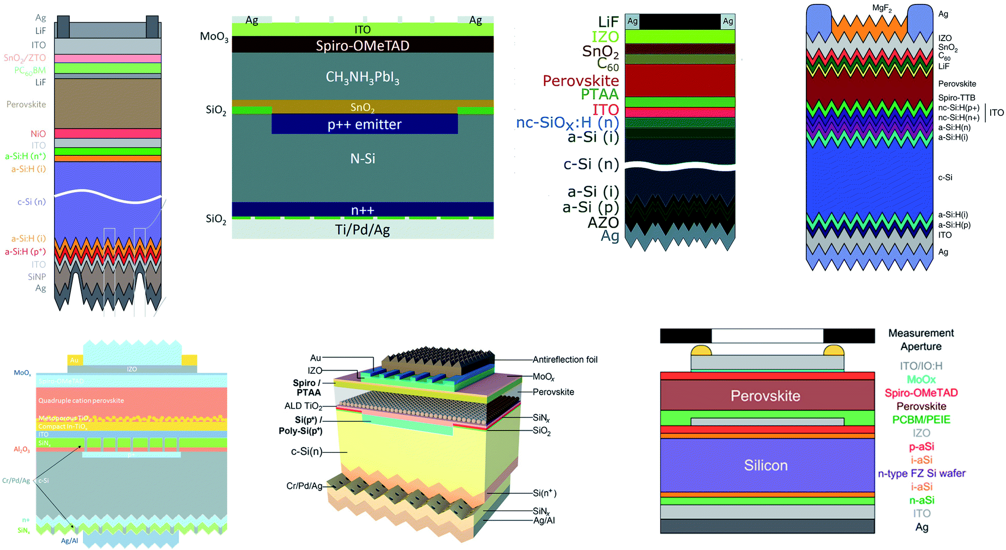 | ||
| Fig. 6 A summary of different 2T tandem structures for large area PVK-based tandem devices.31,97,285,289–293 | ||
| PVK/silicon | ||||||||
|---|---|---|---|---|---|---|---|---|
| Silicon | Perovskite | Top cell bandgap (eV) | Recombination layer | Efficiency (%) | Area (cm2) | Institute | Year | Ref. |
| Homo-junction | MAPbI3 | 1.55 | n++/p++ Si | 13.7 | 1.00 | MIT/stanford | 2015 | 304 |
| MAPbI3 | 1.55 | ZTO | 16.3 | 1.43 | EPFL/CSEM | 2016 | 305 | |
| CsRbFAMAPbI3−xBrx | 1.62 | ITO | 22.5 | 1.00 | ANU | 2017 | 292 | |
| MAPbI3 | 1.58 | — | 21.0 | 4.00 | UNSW | 2018 | 291 | |
| MAPbI3 | 1.58 | — | 17.6 | 16.00 | UNSW | 2018 | 291 | |
| (FAPbI3)0.83(MAPbBr3)0.17 | 1.59 | — | 21.8 | 16.00 | UNSW | 2018 | 291 | |
| CsRbFAMAPbI3−xBrx | 1.62 | — | 23.2 | 1.00 | ANU | 2018 | 285 | |
| FAMAPbI3−xBrx | 1.61 | — | 23.1 | 4.00 | UNSW | 2019 | 303 | |
| SHJ | MAPbI3 | 1.55 | IZO | 19.2 | 1.22 | EPFL/CSEM | 2015 | 290 |
| MAPbI3 | 1.55 | IZO | 20.5 | 1.43 | EPFL/CSEM | 2016 | 283 | |
| CsFAPbI3−xBrx | 1.63 | ITO | 23.6 | 1.00 | Stanford/ASU | 2017 | 289 | |
| CsFAPbI3−xBrx | 1.63 | nc-Si:H | 21.2 | 1.43 | EPFL/CSEM | 2017 | 296 | |
| CsFAPbI3−xBrx | 1.63 | nc-Si:H | 18.0 | 12.96 | EPFL/CSEM | 2017 | 296 | |
| CsFAPbI3−xBrx | 1.63 | nc-Si:H | 25.2 | 1.419 | EPFL/CSEM | 2018 | 97 | |
| CsRbFAMAPbI3−xBrx | 1.62 | — | 24.1 | 1.00 | ANU | 2018 | 285 | |
| CsFAPbI3−xBrx | 1.68 | ITO | 25.0 | 1.00 | Stanford/ASU | 2018 | 300 | |
| CsFAPbI3−xBrx | 1.63 | nc-Si:H | 25.4 | 1.43 | EPFL | 2019 | 306 | |
| Cs0.05(FA0.77MA0.23)0.95Pb(I0.77Br0.23)3 | 1.68 | ITO | 29.1 | 1.06 | HZB | 2020 | 307 | |
| (FA0.65MA0.2Cs0.15)Pb(I0.8Br0.2)3 | 1.68 | ITO | 26.2 | 1.00 | KAIST | 2020 | 308 | |
| FA0.75Cs0.25Pb(I0.8Br0.2)3 | 1.67 | ITO | 27.1 | 1.00 | CU-Boulder | 2020 | 309 | |
| (Cs0.06FA0.78MA0.16)Pb(Br0.17I0.83)3 | 1.64 | ITO | 26.3 | 1.43 | C.H.O.S.E | 2020 | 310 | |
| CsxFA1−xPbIyBr1−y | 1.63 | ITO | 22.6 | 57.4 | CSEM/EPFL | 2019 | 295 | |
| MAPb(I0.75Br0.25)3 | 1.68 | ITO | 23.8 | 1.00 | KSC | 2020 | 288 | |
4.2 Stability of large area PVK-based monolithic tandem devices
Currently, there are some works based on the stability of large-area monolithic tandem devices. The stability of PVK-based monolithic tandem devices is mainly determined by the PVK sub-cell. c-Si is stable enough to operate consistently for many years in ambient conditions. Therefore, the research based on large-area tandem device stability is mainly focused on the top-cell stability improvement. According to recent studies, pinholes are among the factors responsible for device instability. The existence of pinholes leads to film instability because of a decrease in carrier lifetime and mobility.308 To solve this problem, Bush et al.289 applied a bilayer SnO2/ZTO by ALD or pulsed-CVD deposition to prevent the formation of pinholes. The double-layer enables the device to withstand a 1000 hour damp heat test at 85 °C and 85% relative humidity. Another factor is the reaction between the electrode (Ag) and halogens in PVK. Reducing the reaction between PVK and the Ag electrode can also improve the device stability.309 Sahli et al.97 pointed out that buffer layers, as well as a transparent conductive electrode, can efficiently prevent ion migration and suppress the reaction of PVK with the Ag electrode. Besides, a stable carbon or gold electrode can largely improve the device's stability. A third factor impacting stability is moisture/light/temperature-induced environmental degradation. Inorganic materials can be applied to improve thermal stability, such as Cs+ for PVK289 and NiOx for the HTL. As for molecular water, dense buffer layers or transparent polymer layers are introduced to realize a moisture barrier.97,303 In addition, spectrum down-conversion materials are employed to transfer high-energy photons into low energy photons, realizing a device UV stability.303Table 5 summarizes the large area device stabilities in detail. Compared to c-Si solar cells, the stability of PVK-based large area 2T tandem solar cells still needs to be improved further.| Structure | PCE (%) | Area (cm2) | Stability | Ref. |
|---|---|---|---|---|
| CsFAPbI3−xBrxPVK/SHJ | 23.6 | 1.00 | 80% for 1000 h, 85% RH, 85 °C | 289 |
| FA0.75Cs0.25Pb(I0.8Br0.2)3PVK/SHJ | 27.1 | 1.00 | 96% for 1000 hours of MPP operation at 60 °C. | 309 |
| Cs5(MA17FA83)95Pb(I83Br17)3PVK/CIGS | 23.3 | 1.03 | 97% for 11 h, 40 °C, under constant illumination at MPP | 311 |
| CsFAPbI3−xBrxPVK/SHJ | 25.2 | 1.42 | 90% after 270 hours under constant illumination at MPP | 97 |
| FAMAPbI3−xBrxPVK/homojunction | 23.1 | 4.00 | 90% for 288 h, UV exposure | 303 |
| (FAPbI3)0.83(MAPbBr3)0.17PVK/homojunction Si | 21.8 | 16.00 | 91%, for 31 days, room temperature, N2 | 312 |
5. Other issues
5.1 Costs
PVK holds the potential for low-cost production due to the use of abundant material, low processing temperature, and simple deposition methods. The cost of modules is estimated to be around 2 US$ m−2.313 Therefore, the potentially low cost of PSCs has drawn a lot of attention in the PV market. However, the total industrialization costs, especially when the materials, the lifecycle, and energy consumption are taken into consideration, still don't have a conclusive assessment yet. This section will give a brief illustration of the industrialization cost, focusing on manufacturing cost and levelized cost of energy (LCOE).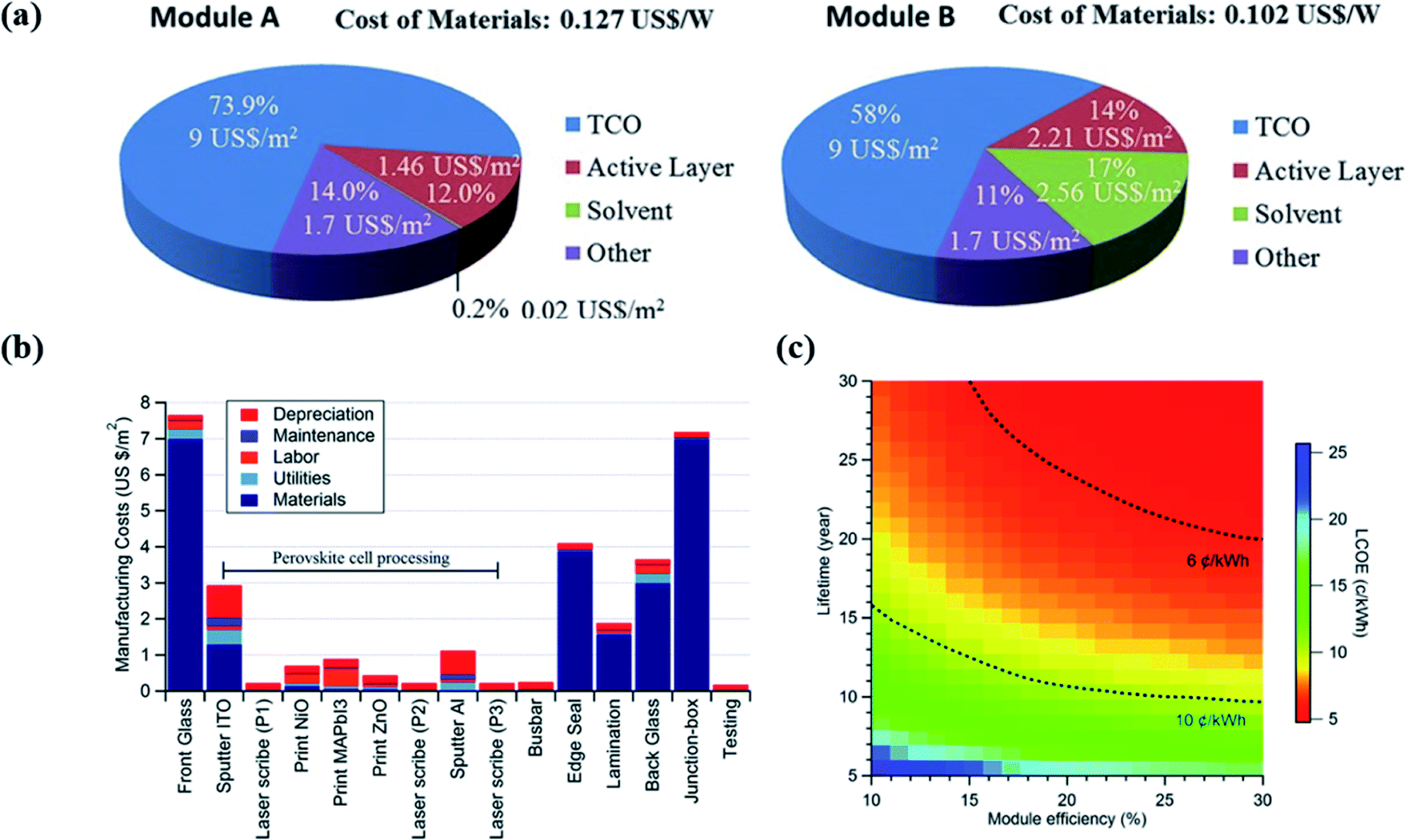 | ||
| Fig. 7 (a) Material cost analysis for two representative examples318 (b) cost contribution of each step for PVK solar modules manufacturing process.319 (c) The relationship between PCE, lifetime, and LCOE for PVK PV modules.314 | ||
Cost modelling is also applied to analyse the PVK/silicon tandem PV technology. Efficiency potential and cost evaluation are accessed in terms of tandem devices and modules. Based on six demonstrated tandem structures, Chang et al.320 found that the cost barriers are in PVK part because of the expensive transporting layer materials. In particular, the use of homojunction cells with p-type wafers helps to decrease the total costs. With similar approach, Messmer et al.321 has an assessment on both PCEs (optical and electrical) and costs based on four promising silicon bottom cell concepts. The detailed comparison between these structures is shown in ref. 321. All these tandem-based cost analysis points out that attentions should be directed to cheaper materials and feasible techniques in the recent future.
The LCOE of PVK/silicon tandem modules is also evaluated, normally together with a detailed comparison of silicon and PVK single junction in reported works.323 By applying this approach, Zafoschnig et al.324 find that PVK/silicon tandem devices have a promising application if the module has a long lifetime and the PCE can exceed 30% using low-cost industrial-scale processes in the next 5–6 years.324 Therefore, the short lifetime of PSCs (compared to more than 25 years for silicon solar cells) and low-cost processing should be especially addressed in near future.325,326
5.2 Perovskite solar cell reproducibility
Although many PSC-related articles have reported high PCEs and excellent stabilities, these data are usually the best or average value over many cells. For the PSC industrialization, efforts based on large-area PVK fabrication need to overcome the reproducibility problem. For different fabrication techniques, device reproducibility is mentioned. Vapor-assisted growth method is indicated to have high reproducibility. Gujar et al.327 demonstrated that 35 devices (36 in total) fabricated with vapor-assisted method worked with very little fluctuation of the photovoltaic parameters (Voc, Jsc, FF and PCE). Following a similar method, Leyden et al.328 and Borchert et al.329 also achieved high device reproducibility for large-area PSCs. In addition, spray coating56 and slot-die coating134 have also been discussed in detail based on large-area PSC reproducibility. Apart from the active layer, the reproducibility of CTLs is also reported.330 PSCs with e-beam evaporated NiOx as HTL show high uniformity and reproducibility.331 However, these studies emphasize the influence of the fabrication technique on reproducibility. Materials should also be taken into consideration for PSC fabrication. Odabası et al.332 assessed the reproducibility by comparing a large number of PSCs using pooled variances (Sp2) comparing different materials and methods. The Sp2 parameters are graphically reported in Fig. 8 and classified by materials that are commonly used in PSCs.332 The reproducibility is higher for lower Sp2 values. This figure provides guidance for identifying the most promising materials for PVK in PV applications. For the ETL, compact SnO2 is an excellent candidate compared with other materials. P3HT and PTAA show smaller Sp2 values compared with spiro-MeOTAD when looking at the HTL. It should be noted that HTL-free devices have also smaller Sp2 values when compared to inorganic HTLs for instance. For common electrode materials reported in this study, the use of carbon results in a higher device reproducibility.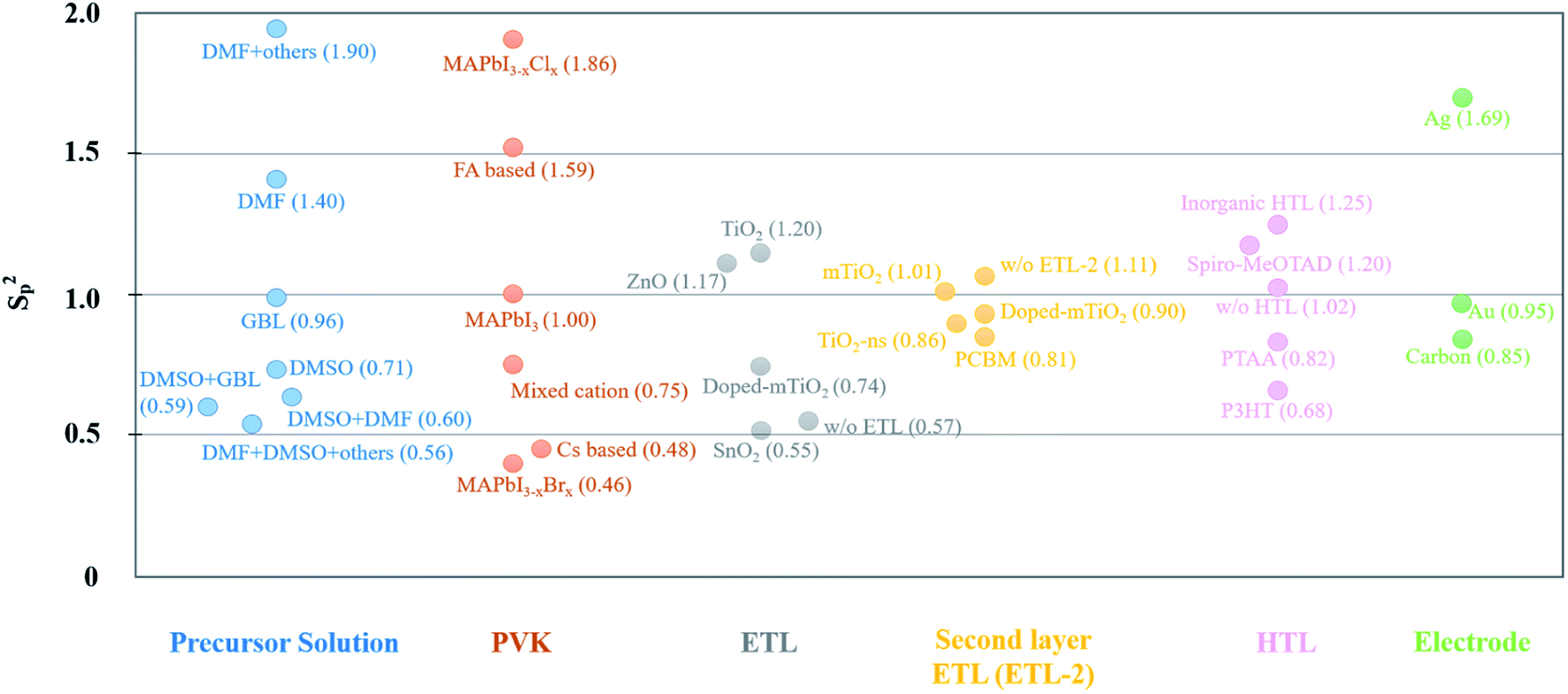 | ||
| Fig. 8 The Sp2 value of materials for each layer of PSCs. The data comes from ref. 332. | ||
5.3 Life cycle assessment
A life cycle assessment (LCA) is employed to evaluate the environmental profile and potential impact of PVK solar modules due to lead toxicity and fabrication exhaust.333 A detailed relationship between PCE, stability and environmental impacts based on PSCs is systematically reviewed by A. Urbina.334 In his work, the author reports different materials and configurations discussing the corresponding environmental impacts.334 Ibn-Mohammed et al.335 reported on the LCA of PVK solar modules based on MAPbX3 and CsFAPbX3. They provide a comparison of a PVK device to other existing PV technologies based on energy consumption, environmental profile and energy payback period (EPBP).335 They pointed out that not only the toxicity of lead, but also the processing of the operating emissions and used materials should be taken into consideration when evaluating the impact on environment. Besides, greenhouse gas emissions factor (GEF) of the PSC, as well as OPV, are much higher than other PV technologies because of their short lifetime, shown in Fig. 9a.335 Therefore, long-term stability indirectly affects energy consumption. In addition, a HTL-free device is also modelled providing excellent LCA results.336Fig. 9b shows the comparison of the PSCs with commercial PV technologies. Environmental impact of global warming potential and primary energy demand are shown as GWP and PED in Fig. 9b.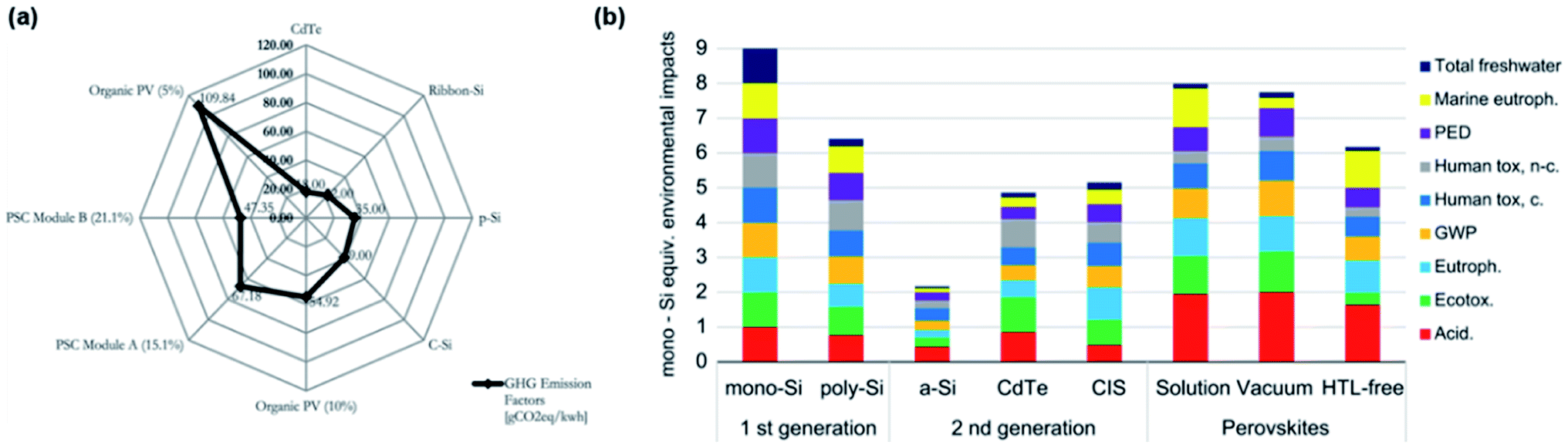 | ||
| Fig. 9 (a) A comparison of GEF based on different PV technologies335 (b) a comparison of environmental impacts based on different factors between PSC and other PV technologies.336 | ||
Moreover, a LCA of PVK-based tandem solar cells has also been modelled.337–339 Tian et al.340 performed a LCA on the EPBP, carbon footprint, and environmental impact scores for both PVK/silicon and PVK/PVK tandem devices. They emphasized that periodic module replacement and material recycling strategies should be implemented to accelerate the application of PVK/silicon tandem devices in PV market.340 To avoid the trouble of module replacement, a method was proposed by Barkhouse et al.341 in 2015. Their modelled results showed that it is important to maintain high infrared transparency and conductivity for the PVK layer after the top cell has stopped working. These properties could ensure that the underlying silicon cell can continue to work without requiring module replacement.341 The detailed discussion and comparison of LCA on PVK/silicon and other single-junctions can be found in Leccisi's review.342
5.4 Summary of companies
With the rapid development towards PSC scaling up, a few companies have been focussing on module fabrication. Most of these companies aim to realize large-area devices (area >100 cm2) mainly using screen printing,235 roll-to-roll printing,343 inkjet-printing344 for the PVK film formation. Besides, some companies fabricate flexible PVK solar modules, such as Toshiba,345 Saule Technologies344 and Energy Materials Corporation.343 Oxford PV has started a manufacturing line for PVK/c-Si tandem cells that are expected to commence production in the year 2021.346 Detailed company information and corresponding progress are summarized in Table 6.| Company name | Country | Efficiency (%) | Area (cm2) | Type of devices | Ref. |
|---|---|---|---|---|---|
| Oxford PV | United Kingdom | 28.0 | 1 | PVK/silicon tandem cells | 346 |
| 29.5 | — | PVK/silicon tandem cells | 352 | ||
| HZB | Germany | 29.8 | 1 | PVK/silicon tandem cells | 34 |
| Greatcell solar | Australia | — | 20 | Focusing on the solar enablement of two substrates: glass and steel, 20 cm2 PVK module | 347 |
| Weihua solar | China | 10.6 | 25 | PVK solar module, carbon electrode, HTL-free | 348 |
| Solliance solar research | Netherlands | 14.5 | 144 | PVK solar module | 66 |
| Microquanta semiconductor | China | 17.9 | 227 | PVK solar module | 235 |
| Solaronix | Switzerland | 12.0 | 500 | PVK solar module | 349 |
| Toshiba | Japan | 11.7 | 703 | PVK flexible solar module | 345 |
| Panasonic | Japan | 16.1 | 802 | PVK solar submodule (55 series cells) | 350 |
| Wonder solar | China | — | 110 × 104 (3600 cm2 for each module) | PVK PV system, screen-printed triple mesoscopic PVK solar modules | 9 |
| Saule Technologies | Poland | — | — | Inkjet-printed flexible PSCs | 344 |
| Energy materials Corporation | United States | — | — | High speed, roll-to-roll printing lines | 343 |
| Swift solar | United States | — | — | All-PVK tandem cells and modules | 351 |
6. Conclusion and outlook
In this review, the developments and challenges for PSCs from lab-to-fab are systematically discussed focusing on different relevant aspects. In the past years, key material processing, scalable device fabrication, and PSC properties have been investigated in depth. However, compared with other well-established PV technologies, both the efficiency and stability of PSCs show a large gap between small-area cells and large-area modules. To achieve the goals of PSCs upscaling and further industrialization, many issues need to be addressed, including not only the efficiency, but also stability, costs, reproducibility, and fabrication techniques. At present, the main challenges involving PSCs commercialization are: (1) long term stability. Modules should ensure durable outdoor operation under operative conditions such as long-term illumination and heat; (2) cost issues. More efforts should be devoted to identify alternative low-cost raw materials for each layer composing the cell, as well as simplifying the device process; (3) further applications. Broad the PSCs application market, for example, tandem device, flexible device, and indoor PV technology. Finally, we are still at the early stage of the PSCs industrialization. In the long term, can PVK realistically become a competitive candidate in the PV market to uptake silicon technology? How the research community will be able to come up with new ideas and solutions aiming at addressing the key challenges/problems we discussed in this review, will indicate the future paths, and define the success of the emerging PVK technology.Conflicts of interest
There are no conflicts to declare.References
- C. Szeles, Phys. Status Solidi B, 2004, 241, 783–790 CrossRef CAS.
- K. Yoshikawa, H. Kawasaki, W. Yoshida, T. Irie, K. Konishi, K. Nakano, T. Uto, D. Adachi, M. Kanematsu, H. Uzu and K. Yamamoto, Nat. Energy, 2017, 2, 17032 CrossRef CAS.
- A. Richter, et al., 10th Int. Conf. Cryst. Silicon Photovoltaics, Leuven, Belgium, Silicon PV, 2020 Search PubMed.
- F. Haase, C. Hollemann, S. Schäfer, A. Merkle, M. Rienäcker, J. Krügener, R. Brendel and R. Peibst, Sol. Energy Mater. Sol. Cells, 2018, 186, 184–193 CrossRef CAS.
- A. Kojima, K. Teshima, Y. Shirai and T. Miyasaka, J. Am. Chem. Soc., 2009, 131, 6050–6051 CrossRef CAS PubMed.
- N. R. E. L. (NREL), Best Research-Cell Efficiency Chart | Photovoltaic Research | NREL.
- S. Agarwal and P. R. Nair, J. Appl. Phys., 2017, 2, 163104 CrossRef.
- J. Yan, N. Li, Y. Ai, Z. Wang, W. Yang, M. Zhao, C. Shou, B. Yan, J. Sheng and J. Ye, Sustainable Energy Fuels, 2019, 3, 3448–3454 RSC.
- Y. Rong, Y. Hu, A. Mei, H. Tan, M. I. Saidaminov, S. Il Seok, M. D. McGehee, E. H. Sargent and H. Han, Science, 2018, 361, 1214–1221 CrossRef CAS PubMed.
- G. Divitini, S. Cacovich, F. Matteocci, L. Cinà, A. Di Carlo and C. Ducati, Nat. Energy, 2016, 1, 15012 CrossRef CAS.
- K. Domanski, E. A. Alharbi, A. Hagfeldt, M. Grätzel and W. Tress, Nat. Energy, 2018, 3, 61–67 CrossRef CAS.
- J. Yang, B. D. Siempelkamp, D. Liu and T. L. Kelly, ACS Nano, 2015, 9, 1955–1963 CrossRef CAS PubMed.
- M. Shirayama, M. Kato, T. Miyadera, T. Sugita, T. Fujiseki, S. Hara, H. Kadowaki, D. Murata, M. Chikamatsu and H. Fujiwara, J. Appl. Phys., 2016, 119, 115501 CrossRef.
- R. K. Misra, S. Aharon, B. Li, D. Mogilyansky, I. Visoly-Fisher, L. Etgar and E. A. Katz, J. Phys. Chem. Lett., 2015, 6, 326–330 CrossRef CAS PubMed.
- X. Tang, M. Brandl, B. May, I. Levchuk, Y. Hou, M. Richter, H. Chen, S. Chen, S. Kahmann, A. Osvet, F. Maier, H. P. Steinrück, R. Hock, G. J. Matt and C. J. Brabec, J. Mater. Chem. A, 2016, 4, 15896–15903 RSC.
- J. Wei, Q. Wang, J. Huo, F. Gao, Z. Gan, Q. Zhao and H. Li, Adv. Energy Mater., 2020, 2002326, 35–37 Search PubMed.
- S. Sun, A. Tiihonen, F. Oviedo, Z. Liu, J. Thapa, Y. Zhao, N. T. P. Hartono, A. Goyal, T. Heumueller, C. Batali, A. Encinas, J. J. Yoo, R. Li, Z. Ren, I. M. Peters, C. J. Brabec, M. G. Bawendi, V. Stevanovic, J. Fisher and T. Buonassisi, Matter, 2021, 4, 1–18 CrossRef.
- T. A. Berhe, W. N. Su, C. H. Chen, C. J. Pan, J. H. Cheng, H. M. Chen, M. C. Tsai, L. Y. Chen, A. A. Dubale and B. J. Hwang, Energy Environ. Sci., 2016, 9, 323–356 RSC.
- C. C. Boyd, R. Cheacharoen, K. A. Bush, R. Prasanna, T. Leijtens and M. D. McGehee, ACS Energy Lett., 2018, 3, 1772–1778 CrossRef CAS.
- J. Carolus, T. Merckx, Z. Purohit, B. Tripathi, H. G. Boyen, T. Aernouts, W. De Ceuninck, B. Conings and M. Daenen, Sol. RRL, 2019, 3, 1–3 Search PubMed.
- C. C. Boyd, R. Cheacharoen, T. Leijtens and M. D. McGehee, Chem. Rev., 2019, 119, 3418–3451 CrossRef CAS PubMed.
- J. Li, J. Huang, A. Zhao, Y. Li and M. Wei, J. Mater. Chem. C, 2020, 8, 8840–8845 RSC.
- R. Chen, Y. Wu, Y. Wang, R. Xu, R. He, Y. Fan, X. Huang, J. Yin, B. Wu, J. Li and N. Zheng, Adv. Funct. Mater., 2020, 2008760, 1–8 Search PubMed.
- G. Tong, D. Y. Son, L. K. Ono, Y. Liu, Y. Hu, H. Zhang, A. Jamshaid, L. Qiu, Z. Liu and Y. Qi, Adv. Energy Mater., 2021, 2003712, 1–11 Search PubMed.
- J. Yang, Q. Hong, Z. Yuan, R. Xu, X. Guo, S. Xiong, X. Liu, S. Braun, Y. Li, J. Tang, C. Duan, M. Fahlman and Q. Bao, Adv. Opt. Mater., 2018, 6, 1–8 Search PubMed.
- M. C. Brennan, S. Draguta, P. V. Kamat and M. Kuno, ACS Energy Lett., 2018, 3, 204–213 CrossRef CAS.
- T. Leijtens, G. E. Eperon, N. K. Noel, S. N. Habisreutinger, A. Petrozza and H. J. Snaith, Adv. Energy Mater., 2015, 5, 1–23 Search PubMed.
- M. Jeong, I. W. Choi, E. M. Go, Y. Cho, M. Kim, B. Lee, S. Jeong, Y. Jo, H. W. Choi, J. Lee, J. H. Bae, S. K. Kwak, D. S. Kim and C. Yang, Science, 2020, 369, 1615–1620 CrossRef CAS PubMed.
- Y. Deng, X. Zheng, Y. Bai, Q. Wang, J. Zhao and J. Huang, Nat. Energy, 2018, 3, 560–566 CrossRef CAS.
- K. Xiao, J. Wen, Q. Han, R. Lin, Y. Gao, S. Gu, Y. Zang, Y. Nie, J. Zhu, J. Xu and H. Tan, ACS Energy Lett., 2020, 5, 2819–2826 CrossRef CAS.
- K. Xiao, R. Lin, Q. Han, Y. Hou, Z. Qin, H. T. Nguyen, J. Wen, M. Wei, V. Yeddu, M. I. Saidaminov, Y. Gao, X. Luo, Y. Wang, H. Gao, C. Zhang, J. Xu, J. Zhu, E. H. Sargent and H. Tan, Nat. Energy, 2020, 5, 870–880 CrossRef CAS.
- J. Wang, V. Zardetto, K. Datta, D. Zhang, M. M. Wienk and R. A. J. Janssen, Nat. Commun., 2020, 11, 1–10 Search PubMed.
- W. Shockley and H. J. Queisser, J. Appl. Phys., 1961, 32, 510–519 CrossRef CAS.
- https://www.pv-magazine.com/2021/11/22/helmholtz-center-achieves-29-80-efficiency-for-perovskite-silicon-tandem-solar-cell/ .
- E. H. Jung, N. J. Jeon, E. Y. Park, C. S. Moon, T. J. Shin, T. Y. Yang, J. H. Noh and J. Seo, Nature, 2019, 567, 511–515 CrossRef CAS PubMed.
- X. Dai, Y. Deng, C. H. Van Brackle, S. Chen, P. N. Rudd, X. Xiao, Y. Lin, B. Chen and J. Huang, Adv. Energy Mater., 2020, 10, 1–7 Search PubMed.
- J. Zhong, W. Wu, L. Ding and D. Kuang, Energy Environ. Mater., 2021, 4, 277–283 CrossRef CAS.
- S. Razza, F. Di Giacomo, F. Matteocci, L. Cinà, A. L. Palma, S. Casaluci, P. Cameron, A. D'Epifanio, S. Licoccia, A. Reale, T. M. Brown and A. Di Carlo, J. Power Sources, 2015, 277, 286–291 CrossRef CAS.
- M. Yang, Z. Li, M. O. Reese, O. G. Reid, D. H. Kim, S. Siol, T. R. Klein, Y. Yan, J. J. Berry, M. F. A. M. Van Hest and K. Zhu, Nat. Energy, 2017, 2, 1–9 Search PubMed.
- A. T. Mallajosyula, K. Fernando, S. Bhatt, A. Singh, B. W. Alphenaar, J. C. Blancon, W. Nie, G. Gupta and A. D. Mohite, Appl. Mater. Today, 2016, 3, 96–102 CrossRef.
- Y. Zhong, R. Munir, J. Li, M.-C. Tang, M. R. Niazi, D.-M. Smilgies, K. Zhao and A. Amassian, ACS Energy Lett., 2018, 3, 1078–1085 CrossRef CAS.
- M. C. Tang, Y. Fan, D. Barrit, X. Chang, H. X. Dang, R. Li, K. Wang, D. M. Smilgies, S. F. Liu, S. De Wolf, T. D. Anthopoulos, K. Zhao and A. Amassian, J. Mater. Chem. A, 2020, 8, 1095–1104 RSC.
- J. Li, R. Munir, Y. Fan, T. Niu, Y. Liu, Y. Zhong, Z. Yang, Y. Tian, B. Liu, J. Sun, D. M. Smilgies, S. Thoroddsen, A. Amassian, K. Zhao and S. (Frank) Liu, Joule, 2018, 2, 1313–1330 CrossRef CAS.
- J. Yin, Y. Lin, C. Zhang, J. Li and N. Zheng, ACS Appl. Mater. Interfaces, 2018, 10, 23103–23111 CrossRef CAS PubMed.
- J. H. Kim, S. T. Williams, N. Cho, C. C. Chueh and A. K. Y. Jen, Adv. Energy Mater., 2015, 5, 2–7 Search PubMed.
- N. G. Park and K. Zhu, Nat. Rev. Mater., 2020, 5, 333–350 CrossRef CAS.
- Z. Ouyang, M. Yang, J. B. Whitaker, D. Li and M. F. A. M. van Hest, ACS Appl. Energy Mater., 2020, 3, 3714–3720 CrossRef CAS.
- S. Chen, X. Dai, S. Xu, H. Jiao, L. Zhao and J. Huang, Science, 2021, 373, 902–907 CrossRef CAS PubMed.
- C. Girotto, D. Moia, B. P. Rand and P. Heremans, Adv. Funct. Mater., 2011, 21, 64–72 CrossRef CAS.
- L. H. Chou, X. F. Wang, I. Osaka, C. G. Wu and C. L. Liu, ACS Appl. Mater. Interfaces, 2018, 10, 38042–38050 CrossRef CAS PubMed.
- A. T. Barrows, A. J. Pearson, C. K. Kwak, A. D. F. Dunbar, A. R. Buckley and D. G. Lidzey, Energy Environ. Sci., 2014, 7, 2944–2950 RSC.
- H. Chen, X. Ding, X. Pan, T. Hayat, A. Alsaedi, Y. Ding and S. Dai, J. Power Sources, 2018, 402, 82–90 CrossRef CAS.
- H. Ishihara, S. Sarang, Y. C. Chen, O. Lin, P. Phummirat, L. Thung, J. Hernandez, S. Ghosh and V. Tung, J. Mater. Chem. A, 2016, 4, 6989–6997 RSC.
- M. Habibi, A. Rahimzadeh, I. Bennouna and M. Eslamian, Coatings, 2017, 7, 42–57 CrossRef.
- Y. S. Chou, L. H. Chou, A. Z. Guo, X. F. Wang, I. Osaka, C. G. Wu and C. L. Liu, ACS Sustainable Chem. Eng., 2019, 7, 14217–14224 CrossRef CAS.
- M. Park, W. Cho, G. Lee, S. C. Hong, M. C. Kim, J. Yoon, N. Ahn and M. Choi, Small, 2019, 15, 1–7 Search PubMed.
- Z. Liang, S. Zhang, X. Xu, N. Wang, J. Wang, X. Wang, Z. Bi, G. Xu, N. Yuan and J. Ding, RSC Adv., 2015, 5, 60562–60569 RSC.
- Z. Bi, Z. Liang, X. Xu, Z. Chai, H. Jin, D. Xu, J. Li, M. Li and G. Xu, Sol. Energy Mater. Sol. Cells, 2017, 162, 13–20 CrossRef CAS.
- J. E. Bishop, J. A. Smith and D. G. Lidzey, ACS Appl. Mater. Interfaces, 2020, 12, 48237–48245 CrossRef CAS PubMed.
- J. H. Heo, F. Zhang, C. Xiao, S. J. Heo, J. K. Park, J. J. Berry, K. Zhu and S. H. Im, Joule, 2021, 5, 481–494 CrossRef CAS.
- D. K. Mohamad, J. Griffin, C. Bracher, A. T. Barrows and D. G. Lidzey, Adv. Energy Mater., 2016, 6, 1–7 Search PubMed.
- E. Bi, W. Tang, H. Chen, Y. Wang, J. Barbaud, T. Wu, W. Kong, P. Tu, H. Zhu, X. Zeng, J. He, S. I. Kan, X. Yang, M. Grätzel and L. Han, Joule, 2019, 3, 2748–2760 CrossRef CAS.
- M. Fievez, P. J. Singh Rana, T. M. Koh, M. Manceau, J. H. Lew, N. F. Jamaludin, B. Ghosh, A. Bruno, S. Cros, S. Berson, S. G. Mhaisalkar and W. L. Leong, Sol. Energy Mater. Sol. Cells, 2021, 230, 111189 CrossRef CAS.
- G. Cotella, J. Baker, D. Worsley, F. De Rossi, C. Pleydell-Pearce, M. Carnie and T. Watson, Sol. Energy Mater. Sol. Cells, 2017, 159, 362–369 CrossRef CAS.
- Solliance, Solliance sets more world records for R2R perovskite solar cells and modules, https://www.solliance.eu/2017/solliance-sets-more-world-records-for-r2r-perovskite-solar-cells-and-modules/.
- F. Di Giacomo, H. Fledderus, H. Gorter, G. Kirchner, I. De Vries, I. Dogan, W. Verhees, V. Zardetto, M. Najafi, D. Zhang, H. Lifka, Y. Galagan, T. Aernouts, S. Veenstra, P. Groen and R. Andriesse, 2018 IEEE 7th World Conf. Photovolt. Energy Conversion, WCPEC 2018-A Jt. Conf. 45th IEEE PVSC, 28th PVSEC 34th EU PVSEC, 2018, pp. 2795–2798 Search PubMed.
- F. Xu, J. Liu, A. S. Subbiah, W. Liu, J. Kang, G. T. Harrison, X. Yang, F. H. Isikgor, E. Aydin, M. De Bastiani and S. De Wolf, Small Sci., 2021, 1, 2000044 CrossRef.
- S. Bernard, S. Jutteau, S. Mejaouri, S. Cacovich, I. Zimmermann, A. Yaiche, S. Gbegnon, D. Loisnard, S. Collin, A. Duchatelet, F. Sauvage and J. Rousset, Sol. RRL, 2021, 5, 1–10 Search PubMed.
- J. Wang, M. R. Squillante, S. Sidhik, A. Mohite and M. S. J. Marshall, 2021 IEEE 48th Photovoltaic Specialists Conference (PVSC), 2021, pp. 1128–1130 Search PubMed.
- I. Zimmermann, M. Al Atem, O. Fournier, S. Bernard, S. Jutteau, L. Lombez and J. Rousset, Adv. Mater. Interfaces, 2021, 8, 1–9 Search PubMed.
- Z. Yang, W. Zhang, S. Wu, H. Zhu, Z. Liu, Z. Liu, Z. Jiang, R. Chen, J. Zhou, Q. Lu, Z. Xiao, L. Shi, H. Chen, L. K. Ono, S. Zhang, Y. Zhang, Y. Qi, L. Han and W. Chen, Sci. Adv., 2021, 7, 1–14 Search PubMed.
- M. Xu, W. Ji, Y. Sheng, Y. Wu, H. Cheng, J. Meng, Z. Yan, J. Xu, A. Mei, Y. Hu, Y. Rong and H. Han, Nano Energy, 2020, 74, 1–8 Search PubMed.
- M. Mercuri, K. Pierpauli, M. G. Bellino and C. L. A. Berli, Langmuir, 2017, 33, 152–157 CrossRef CAS PubMed.
- T. Bu, J. Li, H. Li, C. Tian, J. Su, G. Tong, L. K. Ono, C. Wang, Z. Lin, N. Chai, X. L. Zhang, J. Chang, J. Lu, J. Zhong, W. Huang, Y. Qi, Y. B. Cheng and F. Huang, Science, 2021, 372, 1327–1332 CrossRef CAS PubMed.
- S. H. Huang, C. K. Guan, P. H. Lee, H. C. Huang, C. F. Li, Y. C. Huang and W. F. Su, Adv. Energy Mater., 2020, 10, 1–9 Search PubMed.
- K. Hwang, Y. S. Jung, Y. J. Heo, F. H. Scholes, S. E. Watkins, J. Subbiah, D. J. Jones, D. Y. Kim and D. Vak, Adv. Mater., 2015, 27, 1241–1247 CrossRef CAS PubMed.
- L. Gao, K. Huang, C. Long, F. Zeng, B. Liu and J. Yang, Appl. Phys. A: Mater. Sci. Process., 2020, 126, 1–7 CrossRef.
- F. Di Giacomo, S. Shanmugam, H. Fledderus, B. J. Bruijnaers, W. J. H. Verhees, M. S. Dorenkamper, S. C. Veenstra, W. Qiu, R. Gehlhaar, T. Merckx, T. Aernouts, R. Andriessen and Y. Galagan, Sol. Energy Mater. Sol. Cells, 2018, 181, 53–59 CrossRef CAS.
- R. Patidar, D. Burkitt, K. Hooper, D. Richards and T. Watson, Mater. Today Commun., 2020, 22, 100808 CrossRef CAS.
- Y. Hu, S. Si, A. Mei, Y. Rong, H. Liu, X. Li and H. Han, Sol. RRL, 2017, 1, 2–7 Search PubMed.
- P. Li, C. Liang, B. Bao, Y. Li, X. Hu, Y. Wang, Y. Zhang, F. Li, G. Shao and Y. Song, Nano Energy, 2018, 46, 203–211 CrossRef CAS.
- Z. Li, P. Li, G. Chen, Y. Cheng, X. Pi, X. Yu, D. Yang, L. Han, Y. Zhang and Y. Song, ACS Appl. Mater. Interfaces, 2020, 12, 39082–39091 CrossRef CAS PubMed.
- C. Liang, P. Li, H. Gu, Y. Zhang, F. Li, Y. Song, G. Shao, N. Mathews and G. Xing, Sol. RRL, 2018, 2, 1–9 CAS.
- L. Gil-Escrig, M. Roß, J. Sutter, A. Al-Ashouri, C. Becker and S. Albrecht, Sol. RRL, 2021, 5, 1–9 Search PubMed.
- L. Gil-Escrig, M. Roß, J. Sutter, A. Al-Ashouri, C. Becker and S. Albrecht, Sol. RRL, 2020, 2000553, 1–9 Search PubMed.
- L. Cojocaru, K. Wienands, T. W. Kim, S. Uchida, A. J. Bett, S. Rafizadeh, J. C. Goldschmidt and S. W. Glunz, ACS Appl. Mater. Interfaces, 2018, 10, 26293–26302 CrossRef CAS PubMed.
- P. S. C. Schulze, K. Wienands, A. J. Bett, S. Rafizadeh, L. E. Mundt, L. Cojocaru, M. Hermle, S. W. Glunz, H. Hillebrecht and J. C. Goldschmidt, Thin Solid Films, 2020, 704, 137970 CrossRef CAS.
- C. Gao, J. Liu, C. Liao, Q. Ye, Y. Zhang, X. He, X. Guo, J. Mei and W. Lau, RSC Adv., 2015, 5, 26175–26180 RSC.
- M. Liu, M. B. Johnston and H. J. Snaith, Nature, 2013, 501, 395–398 CrossRef CAS PubMed.
- C.-W. Chen, H.-W. Kang, S.-Y. Hsiao, P.-F. Yang, K.-M. Chiang and H.-W. Lin, Adv. Mater., 2014, 26, 6647–6652 CrossRef CAS PubMed.
- J. Borchert, R. L. Milot, J. B. Patel, C. L. Davies, A. D. Wright, L. Martínez Maestro, H. J. Snaith, L. M. Herz and M. B. Johnston, ACS Energy Lett., 2017, 2, 2799–2804 CrossRef CAS.
- J. Li, H. Wang, X. Y. Chin, H. A. Dewi, K. Vergeer, T. W. Goh, J. W. M. Lim, J. H. Lew, K. P. Loh, C. Soci, T. C. Sum, H. J. Bolink, N. Mathews, S. Mhaisalkar and A. Bruno, Joule, 2020, 4, 1035–1053 CrossRef CAS.
- S. Wang, X. Li, J. Wu, W. Wen and Y. Qi, Curr. Opin. Electrochem., 2018, 11, 130–140 CrossRef CAS.
- J. Werner, F. Sahli, F. Fu, J. J. Diaz Leon, A. Walter, B. A. Kamino, B. Niesen, S. Nicolay, Q. Jeangros and C. Ballif, ACS Energy Lett., 2018, 3, 2052–2058 CrossRef CAS.
- L. Gil-Escrig, C. Dreessen, F. Palazon, Z. Hawash, E. Moons, S. Albrecht, M. Sessolo and H. J. Bolink, ACS Energy Lett., 2021, 6, 827–836 CrossRef CAS PubMed.
- J. Feng, Y. Jiao, H. Wang, X. Zhu, Y. Sun, M. Du, Y. Cao, D. Yang and S. F. Liu, Energy Environ. Sci., 2021, 14, 3035–3043 RSC.
- F. Sahli, J. Werner, B. A. Kamino, M. Bräuninger, R. Monnard, B. Paviet-Salomon, L. Barraud, L. Ding, J. J. Diaz Leon, D. Sacchetto, G. Cattaneo, M. Despeisse, M. Boccard, S. Nicolay, Q. Jeangros, B. Niesen and C. Ballif, Nat. Mater., 2018, 17, 820–826 CrossRef CAS PubMed.
- M. M. Tavakoli and R. Tavakoli, Phys. Status Solidi RRL, 2021, 15, 1–8 Search PubMed.
- Y. Choi, D. Koo, M. Jeong, G. Jeong, J. Lee, B. Lee, K. J. Choi, C. Yang and H. Park, Sol. RRL, 2021, 5, 1–10 Search PubMed.
- T. Lei, F. Li, X. Zhu, H. Dong, Z. Niu, S. Ye, W. Zhao, J. Xi, B. Jiao, L. Ding and Z. Wu, Sol. RRL, 2020, 2000292, 1–9 Search PubMed.
- H. M. Christen and G. Eres, J. Phys.: Condens. Matter, 2008, 20, 264005–264021 CrossRef CAS PubMed.
- S. Hoffmann-Urlaub, Y. Zhang, Z. Wang, B. Kressdorf and T. Meyer, Appl. Phys. A: Mater. Sci. Process., 2020, 126, 1–11 CrossRef.
- U. Bansode and S. Ogale, J. Appl. Phys., 2017, 121, 0021–8979 CrossRef.
- H. Wang, Y. Wu, M. Ma, S. Dong, Q. Li, J. Du, H. Zhang and Q. Xu, ACS Appl. Energy Mater., 2019, 2, 2305–2312 CrossRef CAS.
- V. M. Kiyek, Y. A. Birkhölzer, Y. Smirnov, M. Ledinsky, Z. Remes, J. Momand, B. J. Kooi, G. Koster, G. Rijnders and M. Morales-Masis, Adv. Mater. Interfaces, 2020, 7, 5–9 Search PubMed.
- W. A. Dunlap-Shohl, Y. Zhou, N. P. Padture and D. B. Mitzi, Chem. Rev., 2019, 119, 3193–3295 CrossRef CAS PubMed.
- R. Pate and A. D. Stiff-Roberts, Chem. Phys. Lett., 2009, 477, 406–410 CrossRef CAS.
- T. Soto-Montero, W. Soltanpoor and M. Morales-Masis, APL Mater., 2020, 8, 110903 CrossRef CAS.
- M. R. Leyden, L. K. Ono, S. R. Raga, Y. Kato, S. Wang and Y. Qi, J. Mater. Chem. A, 2014, 2, 18742–18745 RSC.
- M. R. Leyden, Y. Jiang and Y. Qi, J. Mater. Chem. A, 2016, 4, 13125–13132 RSC.
- Y. Jiang, M. R. Leyden, L. Qiu, S. Wang, L. K. Ono, Z. Wu, E. J. Juarez-Perez and Y. Qi, Adv. Funct. Mater., 2018, 28, 1703835 CrossRef.
- L. Luo, Y. Zhang, N. Chai, X. Deng, J. Zhong, F. Huang, Y. Peng, Z. Ku and Y. B. Cheng, J. Mater. Chem. A, 2018, 6, 21143–21148 RSC.
- Y. Jiang, M. Remeika, Z. Hu, E. J. Juarez-Perez, L. Qiu, Z. Liu, T. Kim, L. K. Ono, D. Y. Son, Z. Hawash, M. R. Leyden, Z. Wu, L. Meng, J. Hu and Y. Qi, Adv. Energy Mater., 2019, 9, 1–12 Search PubMed.
- X. Liu, L. Cao, Z. Guo, Y. Li, W. Gao and L. Zhou, Materials, 2019, 12, 1–17 Search PubMed.
- L. Liu, A. Mei, X. Li, H. Han, Y. Dkhissi, A. D. Scully, R. A. Caruso, Y. B. Cheng, I. Jeong, J. Lee, M. J. Ko, K. Yong, B. S. Richards, T. L. Kelly, N. Pellet, M. Levi and S. Turri, Research|reports, 354, 2016.
- L. Qiu, S. He, Y. Jiang, D. Y. Son, L. K. Ono, Z. Liu, T. Kim, T. Bouloumis, S. Kazaoui and Y. Qi, J. Mater. Chem. A, 2019, 7, 6920–6929 RSC.
- H. Chen, F. Ye, W. Tang, J. He, M. Yin, Y. Wang, F. Xie, E. Bi, X. Yang, M. Grätzel and L. Han, Nature, 2017, 550, 92–95 CrossRef CAS PubMed.
- F. Ye, H. Chen, F. Xie, W. Tang, M. Yin, J. He, E. Bi, Y. Wang, X. Yang and L. Han, Energy Environ. Sci., 2016, 9, 2295–2301 RSC.
- P. Li, C. Liang, B. Bao, Y. Li, X. Hu, Y. Wang and Y. Zhang, Nano Energy, 2018, 46, 203–211 CrossRef CAS.
- Z. Li, P. Li, G. Chen, Y. Cheng, X. Pi, X. Yu, D. Yang, L. Han, Y. Zhang and Y. Song, ACS Appl. Mater. Interfaces, 2020, 12, 39082–39091 CrossRef CAS PubMed.
- A. Priyadarshi, L. J. Haur, P. Murray, D. Fu, S. Kulkarni, G. Xing, T. C. Sum, N. Mathews and S. G. Mhaisalkar, Energy Environ. Sci., 2016, 3687–3692 RSC.
- M. R. Leyden, Y. Jiang and Y. Qi, J. Mater. Chem. A, 2016, 4, 13125 RSC.
- L. Luo, Y. Zhang, N. Chai, X. Deng, J. Zhong, F. Huang, Y. Peng, Z. Ku and Y. B. Cheng, J. Mater. Chem. A, 2018, 6, 21143–21148 RSC.
- L. Qiu, S. He, Y. Jiang, D. Son, L. K. Ono, Z. Liu, T. Kim, T. Bouloumis, S. Kazaoui and Y. Qi, J. Mater. Chem. A, 2019, 7, 6920–6929 RSC.
- C. A. M. De Huerta, U. W. Paetzold, R. Gehlhaar, D. Cheyns and P. Heremans, J. Mater. Chem. A, 2016, 4, 3792–3797 RSC.
- Y. Deng, X. Zheng, Y. Bai, Q. Wang, J. Zhao and J. Huang, Nat. Energy, 2018, 3, 560–566 CrossRef CAS.
- H. Huang, J. Shi, L. Zhu, D. Li, Y. Luo and Q. Meng, Nano Energy, 2016, 27, 352–358 CrossRef CAS.
- S. Hyuk, J. Mater. Chem. A, 2016, 4, 17636 RSC.
- L. Cai, L. Liang, J. Wu, B. Ding, L. Gao and B. Fan, J. Semicond., 2017, 38, 014006 CrossRef.
- D. Lee, Y. Jung, Y. Heo, S. Lee, K. Hwang and Y. Jeon, ACS Appl. Mater. Interfaces, 2018, 10, 16133–16139 CrossRef CAS PubMed.
- D. Vak, K. Hwang, A. Faulks, Y. S. Jung, N. Clark, D. Y. Kim, G. J. Wilson and S. E. Watkins, Adv. Energy Mater., 2015, 5, 1–8 Search PubMed.
- Z. Yang, W. Zhang, S. Wu, H. Zhu, Z. Liu, Z. Liu, Z. Jiang, R. Chen, J. Zhou, Q. Lu, Z. Xiao, L. Shi, H. Chen, L. K. Ono, S. Zhang, Y. Zhang, Y. Qi, L. Han and W. Chen, Sci. Adv., 2021, 7, 1–14 Search PubMed.
- F. Di, S. Shanmugam, H. Fledderus, B. J. Bruijnaers, W. J. H. Verhees, M. S. Dorenkamper, S. C. Veenstra and W. Qiu, Sol. Energy Mater. Sol. Cells, 2018, 181, 53–59 CrossRef.
- D. Lee, Y. S. Jung, Y. J. Heo, S. Lee, K. Hwang, Y. J. Jeon, J. E. Kim, J. Park, G. Y. Jung and D. Y. Kim, ACS Appl. Mater. Interfaces, 2018, 10, 16133–16139 CrossRef CAS PubMed.
- Y. Deng, C. H. van Brackle, X. Dai, J. Zhao, B. Chen and J. Huang, Sci. Adv., 2019, 5, 1–9 Search PubMed.
- Y. Deng, Z. Ni, F. Axel and X. Xiao, Joule, 2020, 4, 1949–1960 CrossRef CAS.
- Y. Deng, S. Xu, S. Chen, X. Xiao, J. Zhao and J. Huang, Nat. Energy, 2021, 6, 633–641 CrossRef CAS.
- T. Bu, J. Li, H. Li, C. Tian, J. Su, G. Tong, L. K. Ono, C. Wang, Z. Lin, N. Chai, X. Zhang, J. Chang, J. Lu, J. Zhong, W. Huang, Y. Qi, Y. Cheng and F. Huang, Science, 2021, 372, 1327–1332 CrossRef CAS PubMed.
- J. Li, H. Wang, X. Yu, J. Li, H. Wang, X. Y. Chin, H. A. Dewi, K. Vergeer and T. W. Goh, Joule, 2020, 4, 1035–1053 CrossRef CAS.
- J. Feng, Y. Jiao, H. Wang, X. Zhu, Y. Sun, M. Du, Y. Cao, D. Yang and S. F. Liu, Energy Environ. Sci., 2021, 14, 3035–3043 RSC.
- T. Lei, F. Li, X. Zhu, H. Dong, Z. Niu, S. Ye, W. Zhao, J. Xi, B. Jiao, L. Ding and Z. Wu, Sol. RRL, 2020, 2000292, 1–9 Search PubMed.
- Z. Yang, S. Zhang, L. Li and W. Chen, J Materiomics., 2017, 3, 231–244 CrossRef.
- Y. Rong, S. Venkatesan, R. Guo, Y. Wang, J. Bao, W. Li, Z. Fan and Y. Yao, Nanoscale, 2016, 8, 12892–12899 RSC.
- G. Longo, A. Wong, M. Sessolo and H. J. Bolink, J. Lumin., 2017, 189, 120–125 CrossRef CAS.
- C. Roldán-Carmona, P. Gratia, I. Zimmermann, G. Grancini, P. Gao, M. Graetzel and M. K. Nazeeruddin, Energy Environ. Sci., 2015, 8, 3550–3556 RSC.
- D. H. Kim, J. B. Whitaker, Z. Li, M. F. A. M. van Hest and K. Zhu, Joule, 2018, 2, 1437–1451 CrossRef CAS.
- M. Jung, S. G. Ji, G. Kim and S. Il Seok, Chem. Soc. Rev., 2019, 48, 2011–2038 RSC.
- Y. Deng, E. Peng, Y. Shao, Z. Xiao, Q. Dong and J. Huang, Energy Environ. Sci., 2015, 8, 1544–1550 RSC.
- Q. Wang, M. Eslamian, T. Zhao and A. K. Y. Jen, IEEE J. Photovoltaics, 2018, 8, 1662–1669 Search PubMed.
- S. Chen, X. Xiao, H. Gu and J. Huang, Sci. Adv., 2021, 7, 1–7 Search PubMed.
- W. Q. Wu, Z. Yang, P. N. Rudd, Y. Shao, X. Dai, H. Wei, J. Zhao, Y. Fang, Q. Wang, Y. Liu, Y. Deng, X. Xiao, Y. Feng and J. Huang, Sci. Adv., 2019, 5, 1–10 Search PubMed.
- Z. Xu, R. Chen, Y. Wu, R. He, J. Yin, W. Lin, B. Wu, J. Li and N. Zheng, J. Mater. Chem. A, 2019, 7, 26849–26857 RSC.
- J. Su, H. Cai, J. Yang, X. Ye, R. Han, J. Ni, J. Li and J. Zhang, ACS Appl. Mater. Interfaces, 2020, 12, 3531–3538 CrossRef CAS PubMed.
- J. E. Bishop, T. J. Routledge and D. G. Lidzey, J. Phys. Chem. Lett., 2018, 9, 1977–1984 CrossRef CAS PubMed.
- J. H. Heo, M. H. Lee, M. H. Jang and S. H. Im, J. Mater. Chem. A, 2016, 4, 17636–17642 RSC.
- J. Li, J. Dagar, O. Shargaieva, M. A. Flatken, H. Köbler, M. Fenske, C. Schultz, B. Stegemann, J. Just, D. M. Többens, A. Abate, R. Munir and E. Unger, Adv. Energy Mater., 2021, 11, 2003460 CrossRef CAS.
- Y. Galagan, F. Di Giacomo, H. Gorter, G. Kirchner, I. de Vries, R. Andriessen and P. Groen, Adv. Energy Mater., 2018, 8, 1–7 Search PubMed.
- D. Burkitt, R. Patidar, P. Greenwood, K. Hooper, J. McGettrick, S. Dimitrov, M. Colombo, V. Stoichkov, D. Richards, D. Beynon, M. Davies and T. Watson, Sustainable Energy Fuels, 2020, 4, 3340–3351 RSC.
- G. Cotella, J. Baker, D. Worsley, F. De Rossi, C. Pleydell-Pearce, M. Carnie and T. Watson, Sol. Energy Mater. Sol. Cells, 2017, 159, 362–369 CrossRef CAS.
- D. Burkitt, R. Swartwout, J. McGettrick, P. Greenwood, D. Beynon, R. Brenes, V. Bulović and T. Watson, RSC Adv., 2019, 9, 37415–37423 RSC.
- F. Mathies, T. Abzieher, A. Hochstuhl, K. Glaser, A. Colsmann, U. W. Paetzold, G. Hernandez-Sosa, U. Lemmer and A. Quintilla, J. Mater. Chem. A, 2016, 4, 19207–19213 RSC.
- C. Zuo, D. Vak, D. Angmo, L. Ding and M. Gao, Nano Energy, 2018, 46, 185–192 CrossRef CAS.
- L. Zhang, S. Chen, X. Wang, D. Wang, Y. Li, Q. Ai, X. Sun, J. Chen, Y. Li, X. Jiang, S. Yang and B. Xu, Sol. RRL, 2021, 5, 1–11 Search PubMed.
- A. Giuri, E. Saleh, A. Listorti, S. Colella, A. Rizzo, C. Tuck and C. E. Corcione, Nanomaterials, 2019, 9, 582–594 CrossRef CAS PubMed.
- B. Dou, J. B. Whitaker, K. Bruening, D. T. Moore, L. M. Wheeler, J. Ryter, N. J. Breslin, J. J. Berry, S. M. Garner, F. S. Barnes, S. E. Shaheen, C. J. Tassone, K. Zhu and M. F. A. M. Van Hest, ACS Energy Lett., 2018, 3, 2558–2565 CrossRef CAS.
- L. Qiu, S. He, L. K. Ono, S. Liu and Y. Qi, ACS Energy Lett., 2019, 4, 2147–2167 CrossRef CAS.
- D. K. Lee, K. S. Lim, J. W. Lee and N. G. Park, J. Mater. Chem. A, 2021, 9, 3018–3028 RSC.
- M. Zhang, D. Xin, X. Zheng, Q. Chen and W. H. Zhang, ACS Sustainable Chem. Eng., 2020, 8, 13126–13138 CrossRef CAS.
- Y. Vaynzof, Adv. Energy Mater., 2020, 10, 2003073 CrossRef CAS.
- C. Roldán-Carmona, O. Malinkiewicz, A. Soriano, G. Mínguez Espallargas, A. Garcia, P. Reinecke, T. Kroyer, M. I. Dar, M. K. Nazeeruddin and H. J. Bolink, Energy Environ. Sci., 2014, 7, 994–997 RSC.
- M. H. Li, C. W. Hsu, P. S. Shen, H. M. Cheng, Y. Chi, P. Chen and T. F. Guo, Chem. Commun., 2015, 51, 15518–15521 RSC.
- Z. Hawash, L. K. Ono and Y. Qi, Adv. Mater. Interfaces, 2018, 5, 1700623 CrossRef.
- D. Luo, W. Yang, Z. Wang, A. Sadhanala, Q. Hu, R. Su, R. Shivanna, G. F. Trindade, J. F. Watts, Z. Xu, T. Liu, K. Chen, F. Ye, P. Wu, L. Zhao, J. Wu, Y. Tu, Y. Zhang, X. Yang, W. Zhang, R. H. Friend, Q. Gong, H. J. Snaith and R. Zhu, Science, 2018, 360, 1442–1446 CrossRef CAS PubMed.
- M. M. Tavakoli and R. Tavakoli, Phys. Status Solidi RRL, 2020, 2000449, 2000449 Search PubMed.
- A. C. Nkele, A. C. Nwanya, N. M. Shinde, S. Ezugwu, M. Maaza, J. S. Shaikh and F. I. Ezema, Int. J. Energy Res., 2020, 44, 9839–9863 CrossRef CAS.
- K. Cao, Z. Zuo, J. Cui, Y. Shen, T. Moehl, S. M. Zakeeruddin, M. Grätzel and M. Wang, Nano Energy, 2015, 17, 171–179 CrossRef CAS.
- X. Yin, M. Que, Y. Xing and W. Que, J. Mater. Chem. A, 2015, 3, 24495–24503 RSC.
- W. J. Scheideler, N. Rolston, O. Zhao, J. Zhang and R. H. Dauskardt, Adv. Energy Mater., 2019, 9, 1–8 Search PubMed.
- T. Abzieher, S. Moghadamzadeh, F. Schackmar, H. Eggers, F. Sutterlüti, A. Farooq, D. Kojda, K. Habicht, R. Schmager, A. Mertens, R. Azmi, L. Klohr, J. A. Schwenzer, M. Hetterich, U. Lemmer, B. S. Richards, M. Powalla and U. W. Paetzold, Adv. Energy Mater., 2019, 9, 1–13 Search PubMed.
- X. Liu, Y. Xiao, Q. Zeng, J. Jiang and Y. Li, J. Phys. Chem. Lett., 2019, 10, 6382–6388 CrossRef CAS PubMed.
- B. S. Kim, T. M. Kim, M. S. Choi, H. S. Shim and J. J. Kim, Org. Electron., 2015, 17, 102–106 CrossRef CAS.
- B. Xie, Y. Zhang, Y. Li, W. Chen, X. Hu and S. Zhang, J. Mater. Sci.: Mater. Electron., 2020, 31, 6248–6254 CrossRef CAS.
- A. M. Igual-Muñoz, J. Ávila, P. P. Boix and H. J. Bolink, Sol. RRL, 2020, 4, 1–5 Search PubMed.
- Q. Zeng, Z. Xu, C. Zheng, Y. Liu, W. Chen, T. Guo, F. Li, C. Xiang, Y. Yang, W. Cao, X. Xie, X. Yan, L. Qian and P. H. Holloway, ACS Appl. Mater. Interfaces, 2018, 10, 8258–8264 CrossRef CAS PubMed.
- W. Zhang, H. Li, C. J. Firby, M. Al-Hussein and A. Y. Elezzabi, ACS Appl. Mater. Interfaces, 2019, 11, 20378–20385 CrossRef CAS PubMed.
- A. Ng, Z. Ren, Q. Shen, S. H. Cheung, H. C. Gokkaya, G. Bai, J. Wang, L. Yang, S. K. So, A. B. Djurišić, W. W. F. Leung, J. Hao, W. K. Chan and C. Surya, J. Mater. Chem. A, 2015, 3, 9223–9231 RSC.
- Y. Zhao, A. M. Nardes and K. Zhu, Appl. Phys. Lett., 2014, 104, 213906 CrossRef.
- P. Schulz, J. O. Tiepelt, J. A. Christians, I. Levine, E. Edri, E. M. Sanehira, G. Hodes, D. Cahen and A. Kahn, ACS Appl. Mater. Interfaces, 2016, 8, 31491–31499 CrossRef CAS PubMed.
- I. S. Yang, M. R. Sohn, S. Do Sung, Y. J. Kim, Y. J. Yoo, J. Kim and W. I. Lee, Nano Energy, 2017, 32, 414–421 CrossRef CAS.
- J. A. Raiford, R. A. Belisle, K. A. Bush, R. Prasanna, A. F. Palmstrom, M. D. McGehee and S. F. Bent, Sustainable Energy Fuels, 2019, 3, 1517–1525 RSC.
- S. Chu, R. Zhao, R. Liu, Y. Gao, X. Wang, C. Liu, J. Chen and H. Zhou, Semicond. Sci. Technol., 2018, 33, 115016 CrossRef.
- D. Forgács, L. Gil-Escrig, D. Pérez-Del-Rey, C. Momblona, J. Werner, B. Niesen, C. Ballif, M. Sessolo and H. J. Bolink, Adv. Energy Mater., 2017, 7, 1–6 Search PubMed.
- Y. Zheng, J. Kong, D. Huang, W. Shi, L. Mcmillon-Brown, H. E. Katz, J. Yu and A. D. Taylor, Nanoscale, 2018, 10, 11342–11348 RSC.
- Z. Yang, C. C. Chueh, F. Zuo, J. H. Kim, P. W. Liang and A. K. Y. Jen, Adv. Energy Mater., 2015, 5, 1–6 CAS.
- Z. Ku, Y. Rong, M. Xu, T. Liu and H. Han, Sci. Rep., 2013, 3, 3132–3137 CrossRef PubMed.
- Y. Yang, K. Ri, A. Mei, L. Liu, M. Hu, T. Liu, X. Li and H. Han, J. Mater. Chem. A, 2015, 3, 9103–9107 RSC.
- B. Su, H. A. Caller-Guzman, V. Körstgens, Y. Rui, Y. Yao, N. Saxena, G. Santoro, S. V. Roth and P. Müller-Buschbaum, ACS Appl. Mater. Interfaces, 2017, 9, 43724–43732 CrossRef CAS PubMed.
- K. S. Keremane, S. Prathapani, L. J. Haur, A. Bruno, A. Priyadarshi, A. V. Adhikari and S. G. Mhaisalkar, ACS Appl. Energy Mater., 2021, 2–11 Search PubMed.
- P. Chen, Z. Wang, S. Wang, M. Lyu, M. Hao, M. Ghasemi, M. Xiao, J. H. Yun, Y. Bai and L. Wang, Nano Energy, 2020, 69, 104392 CrossRef CAS.
- Q. Jiang, Y. Zhao, X. Zhang, X. Yang, Y. Chen, Z. Chu, Q. Ye, X. Li, Z. Yin and J. You, Nat. Photonics, 2019, 13, 460–466 CrossRef CAS.
- Z. Ku, X. Xia, H. Shen, N. H. Tiep and H. J. Fan, Nanoscale, 2015, 7, 13363–13368 RSC.
- S. H. Lee, G. Kim, J. W. Lim, K. S. Lee and M. G. Kang, Sol. Energy Mater. Sol. Cells, 2018, 186, 378–384 CrossRef CAS.
- C. Tian, A. Mei, S. Zhang, H. Tian, S. Liu, F. Qin, Y. Xiong, Y. Rong, Y. Hu, Y. Zhou, S. Xie and H. Han, Nano Energy, 2018, 53, 160–167 CrossRef CAS.
- H. Chen and S. Yang, Adv. Mater., 2017, 29, 1603994 CrossRef PubMed.
- T. Mahmoudi, Y. Wang and Y. B. Hahn, Nano Energy, 2018, 47, 51–65 CrossRef CAS.
- E. L. Lim, C. C. Yap, M. H. H. Jumali, M. A. M. Teridi and C. H. Teh, Nano-Micro Lett., 2018, 10, 27–39 CrossRef PubMed.
- Z. Liu, P. You, C. Xie, G. Tang and F. Yan, Nano Energy, 2016, 28, 151–157 CrossRef CAS.
- H. Sung, N. Ahn, M. S. Jang, J. K. Lee, H. Yoon, N. G. Park and M. Choi, Adv. Energy Mater., 2016, 6, 2–7 Search PubMed.
- J. Yoon, H. Sung, G. Lee, W. Cho, N. Ahn, H. S. Jung and M. Choi, Energy Environ. Sci., 2017, 10, 337–345 RSC.
- C. Zhang, S. Wang, H. Zhang, Y. Feng, W. Tian, Y. Yan, J. Bian, Y. Wang, S. Jin, S. M. Zakeeruddin, M. Grätzel and Y. Shi, Energy Environ. Sci., 2019, 12, 3585–3594 RSC.
- Y. Yuan and J. Huang, Acc. Chem. Res., 2016, 49, 286–293 CrossRef CAS PubMed.
- M. I. Asghar, J. Zhang, H. Wang and P. D. Lund, Renewable Sustainable Energy Rev., 2017, 77, 131–146 CrossRef CAS.
- N. A. N. Ouedraogo, Y. Chen, Y. Y. Xiao, Q. Meng, C. B. Han, H. Yan and Y. Zhang, Nano Energy, 2020, 67, 104249 CrossRef CAS.
- Y. Wang, Y. Zhou, T. Zhang, M. G. Ju, L. Zhang, M. Kan, Y. Li, X. C. Zeng, N. P. Padture and Y. Zhao, Mater. Horiz., 2018, 5, 868–873 RSC.
- A. Agresti, S. Pescetelli, A. L. Palma, B. Martín-García, L. Najafi, S. Bellani, I. Moreels, M. Prato, F. Bonaccorso and A. Di Carlo, ACS Energy Lett., 2019, 4, 1862–1871 CrossRef CAS.
- J. Liu, Y. Xue, Z. Wang, Z. Q. Xu, C. Zheng, B. Weber, J. Song, Y. Wang, Y. Lu, Y. Zhang and Q. Bao, ACS Nano, 2016, 10, 3536–3542 CrossRef CAS PubMed.
- J. Wu, J. Shi, Y. Li, H. Li, H. Wu and Y. Luo, Adv. Energy Mater., 2019, 1901352, 1–9 Search PubMed.
- X. Ren, L. Zhang, Y. Yuan and L. Ding, J. Semicond., 2021, 42, 010201 CrossRef CAS.
- H. Yu, Q. Sun, T. Zhang, X. Zhang, Y. Shen and M. Wang, Mater. Today Energy, 2021, 19, 1–12 Search PubMed.
- E. Zheng, Z. Niu, G. A. Tosado, H. Dong, Y. Albrikan and Q. Yu, J. Phys. Chem. C, 2020, 124, 18805–18815 CrossRef CAS.
- K. J. Xu, R. T. Wang, A. F. Xu, J. Y. Chen and G. Xu, ACS Appl. Mater. Interfaces, 2020, 12, 48882–48889 CrossRef CAS PubMed.
- S. P. Russo and N. V Medhekar, J. Mater. Chem. A, 2020, 8, 17765–17779 RSC.
- S. Fang, W. Yao, Z. Hu, L. Huang, X. Liu, H. Zhang, J. Zhang and Y. Zhu, J. Phys. Chem. C, 2021, 125, 21370–21380 CrossRef CAS.
- S. Bae, S. Kim, S. Lee, K. J. Cho, S. Park, S. Lee, Y. Kang, H. Lee and D. Kim, J. Phys. Chem. Lett., 2016, 7, 3091–3096 CrossRef CAS PubMed.
- P. Bastos, W. Song, L. Rakocevic, R. T. Eachambadi, W. Qiu, R. Gehlhaar, Y. Kuang, A. Hadipour, T. Aernouts and J. Poortmans, ACS Appl. Mater. Interfaces, 2021, 13, 44294–44301 CrossRef PubMed.
- F. Wan, X. Qiu, H. Chen, Y. Liu, H. Xie, J. Shi and H. Huang, Org. Electron., 2018, 59, 184–189 CrossRef CAS.
- W. Ming, D. Yang, T. Li, L. Zhang and M. Du, Adv. Sci., 2018, 5, 1700662 CrossRef PubMed.
- O. A. Syzgantseva, M. Saliba, M. Gra and U. Rothlisberger, Sci. Rep., 2017, 7, 6–11 CrossRef PubMed.
- S. Tang, S. Huang, G. J. Wilson and A. Ho-baillie, Trends Chem., 2006, 2, 638–653 CrossRef.
- S. Bi, X. Leng, Y. Li, Z. Zheng, X. Zhang and Y. Zhang, Adv. Mater., 2019, 31, 1–8 CrossRef PubMed.
- A. Agresti, S. Pescetelli, A. L. Palma, B. Mart, L. Naja, S. Bellani, I. Moreels, M. Prato, F. Bonaccorso and A. Di Carlo, ACS Energy Lett., 2019, 4, 1862–1871 CrossRef CAS.
- J. You, L. Meng, T. Bin Song, T. F. Guo, W. H. Chang, Z. Hong, H. Chen, H. Zhou, Q. Chen, Y. Liu, N. De Marco and Y. Yang, Nat. Nanotechnol., 2016, 11, 75–81 CrossRef CAS PubMed.
- W. Sun, Y. Li, S. Ye, H. Rao, W. Yan, H. Peng, Y. Li, Z. Liu, S. Wang, Z. Chen, L. Xiao, Z. Bian and C. Huang, Nanoscale, 2016, 8, 10806–10813 RSC.
- S. Ye, W. Sun, Y. Li, W. Yan, H. Peng, Z. Bian, Z. Liu and C. Huang, Nano Lett., 2015, 15, 3723–3728 CrossRef CAS PubMed.
- Microquanta demonstrates high stability beyond IEC standards, http://www.microquanta.com/en/newsinfo/112E5B4ABC180F9D/.
- M. V. Khenkin, E. A. Katz, A. Abate, G. Bardizza, J. J. Berry, C. Brabec, F. Brunetti, V. Bulović, Q. Burlingame, A. Di Carlo, R. Cheacharoen, Y. B. Cheng, A. Colsmann, S. Cros, K. Domanski, M. Dusza, C. J. Fell, S. R. Forrest, Y. Galagan, D. Di Girolamo, M. Grätzel, A. Hagfeldt, E. von Hauff, H. Hoppe, J. Kettle, H. Köbler, M. S. Leite, S. (Frank) Liu, Y. L. Loo, J. M. Luther, C. Q. Ma, M. Madsen, M. Manceau, M. Matheron, M. McGehee, R. Meitzner, M. K. Nazeeruddin, A. F. Nogueira, Ç. Odabaşı, A. Osherov, N. G. Park, M. O. Reese, F. De Rossi, M. Saliba, U. S. Schubert, H. J. Snaith, S. D. Stranks, W. Tress, P. A. Troshin, V. Turkovic, S. Veenstra, I. Visoly-Fisher, A. Walsh, T. Watson, H. Xie, R. Yıldırım, S. M. Zakeeruddin, K. Zhu and M. Lira-Cantu, Nat. Energy, 2020, 5, 35–49 CrossRef.
- Z. Yang, S. Zhang, L. Li and W. Chen, J. Mater., 2017, 3, 231–244 Search PubMed.
- N. Li, X. Niu, Q. Chen and H. Zhou, Chem. Soc. Rev., 2020, 49, 8235–8286 RSC.
- Q. Wali, F. J. Iftikhar, M. E. Khan, A. Ullah, Y. Iqbal and R. Jose, Org. Electron., 2020, 78, 105590 CrossRef CAS.
- S. Zhang, Z. Liu, W. Zhang, Z. Jiang, W. Chen, R. Chen, Y. Huang, Z. Yang, Y. Zhang, L. Han and W. Chen, Adv. Energy Mater., 2020, 10, 1–49 Search PubMed.
- M. K. Rao, D. N. Sangeetha, M. Selvakumar, Y. N. Sudhakar and M. G. Mahesha, Sol. Energy, 2021, 218, 469–491 CrossRef.
- U. Krishnan, J. Photonics Energy, 2019, 9, 1 Search PubMed.
- A. Priyadarshi, L. J. Haur, P. Murray, D. Fu, S. Kulkarni, G. Xing, T. C. Sum, N. Mathews and S. G. Mhaisalkar, Energy Environ. Sci., 2016, 9, 3687–3692 RSC.
- A. Mei, X. Li, L. Liu, Z. Ku, T. Liu, Y. Rong, M. Xu, M. Hu, J. Chen, Y. Yang, M. Grätzel and H. Han, Science, 2014, 345, 295–298 CrossRef CAS PubMed.
- H. Tan, E. Moulin, T. F. Si, J.-W. Schüttauf, M. Stuckelberger, O. Isabella, F. J. Haug, C. Ballif, M. Zeman and A. H. M. Smets, Prog. Photovolt. Res. Appl., 2015, 23, 949–963 CrossRef CAS.
- T. Matsui, K. Maejima, A. Bidiville, H. Sai, T. Koida, T. Suezaki, M. Matsumoto, K. Saito, I. Yoshida and M. Kondo, Jpn. J. Appl. Phys., 2015, 54, 10–14 Search PubMed.
- J. S. Cashmore, M. Apolloni, A. Braga, O. Caglar, V. Cervetto, Y. Fenner, S. Goldbach-Aschemann, C. Goury, J. E. Hötzel, T. Iwahashi, J. Kalas, M. Kitamura, M. Klindworth, M. Kupich, G. F. Leu, J. Lin, M. H. Lindic, P. A. Losio, T. Mates, D. Matsunaga, B. Mereu, X. V. Nguyen, I. Psimoulis, S. Ristau, T. Roschek, A. Salabas, E. L. Salabas and I. Sinicco, Sol. Energy Mater. Sol. Cells, 2016, 144, 84–95 CrossRef CAS.
- S. Kim, J. W. Chung, H. Lee, J. Park, Y. Heo and H. M. Lee, Sol. Energy Mater. Sol. Cells, 2013, 119, 26–35 CrossRef CAS.
- B. Liu, L. Bai, Z. Chen, X. Zhang, D. Zhang, J. Ni, Q. Huang, C. Wei, J. Sun, X. Chen, H. Ren, G. Hou, G. Wang and Y. Zhao, Prog. Photovolt. Res. Appl., 2015, 23, 1313–1322 CrossRef CAS.
- K. Söderström, G. Bugnon, R. Biron, C. Pahud, F. Meillaud, F. J. Haug and C. Ballif, J. Appl. Phys., 2012, 112, 114503 CrossRef.
- B. Yan, G. Yue, L. Sivec, J. Yang, S. Guha and C. S. Jiang, Appl. Phys. Lett., 2011, 99, 113512 CrossRef.
- H. Sai, T. Matsui and K. Matsubara, Appl. Phys. Lett., 2016, 109, 1–6 Search PubMed.
- F. J. Haug and C. Ballif, Energy Environ. Sci., 2015, 8, 824–837 RSC.
- O. Isabella, A. H. M. Smets and M. Zeman, Sol. Energy Mater. Sol. Cells, 2014, 129, 82–89 CrossRef CAS.
- F. T. Si, D. Y. Kim, R. Santbergen, H. Tan, R. A. C. M. M. Van Swaaij, A. H. M. Smets, O. Isabella and M. Zeman, Appl. Phys. Lett., 2014, 105, 063902 CrossRef.
- S. Kirner, S. Neubert, C. Schultz, O. Gabriel, B. Stannowski, B. Rech and R. Schlatmann, Jpn. J. Appl. Phys., 2015, 54, 03 CrossRef.
- M. Konagai, H. Noge and R. Ishikawa, Prog. Photovolt. Res. Appl., 2020, 1–7 Search PubMed.
- T. Takamoto, H. Washio and H. Huso, Proc. 40 th IEEE PVSC, 2014, pp. 5–9 Search PubMed.
- N. Jain, K. L. Schulte, J. F. Geisz, D. J. Friedman, R. M. France, E. E. Perl, A. G. Norman, H. L. Guthrey and M. A. Steiner, Appl. Phys. Lett., 2018, 112, 053905 CrossRef.
- F. Dimroth, T. N. D. Tibbits, M. Niemeyer, F. Predan, P. Beutel, C. Karcher, E. Oliva, G. Siefer, D. Lackner, P. Fus-Kailuweit, A. W. Bett, R. Krause, C. Drazek, E. Guiot, J. Wasselin, A. Tauzin and T. Signamarcheix, IEEE J. Photovoltaics, 2016, 6, 343–349 Search PubMed.
- J. F. Geisz, M. A. Steiner, N. Jain, K. L. Schulte, R. M. France, W. E. McMahon, E. E. Perl and D. J. Friedman, IEEE J. Photovoltaics, 2018, 8, 626–632 Search PubMed.
- K. Sasaki, T. Agui, K. Nakaido, N. Takahashi, R. Onitsuka and T. Takamoto, AIP Conf. Proc., 2013, 1556, 22–25 CrossRef CAS.
- P. T. Chiu, D. C. Law, R. L. Woo, S. B. Singer, D. Bhusari, W. D. Hong, A. Zakaria, J. Boisvert, S. Mesropian, R. R. King and N. H. Karam, 2014 IEEE 40th Photovolt. Spec. Conf. PVSC 2014, 2014, pp. 11–13 Search PubMed.
- MicroLink Device Inc, MicroLink AFWERX Phase I Projects, 2021 Search PubMed.
- NREL, News Release: NREL Demonstrates 45.7% Efficiency for Concentrator Solar Cell, 2014 Search PubMed.
- SHARP, Sharp Develops Concentrator Solar Cell with World's Highest Conversion Efficiency of 43.5%, 2012 Search PubMed.
- Z. Yu, M. Leilaeioun and Z. Holman, Nat. Energy, 2016, 1, 16137 CrossRef.
- E. L. Warren, W. E. Mcmahon, M. Rienäcker, K. T. Vansant, R. C. Whitehead, R. Peibst and A. C. Tamboli, ACS Energy Lett., 2020, 5, 1233–1242 CrossRef CAS.
- M. Rienäcker, E. L. Warren, M. Schnabel, H. Schulte-Huxel, R. Niepelt, R. Brendel, P. Stradins, A. C. Tamboli and R. Peibst, Prog. Photovolt. Res. Appl., 2019, 27, 410–423 CrossRef.
- J. P. Connolly, K. Ahanobge, J.-P. Kleider, J. Alvarez, H. Kanda, M. Nazeeruddin, V. Mihailetchi, P. Baranek, M. Vogt, R. Santbergen, J. P. Kleider, M. K. Nazeeruddin, V. Mihailetchi, P. Baranek and O. Isabella, 37th European Photovoltaic Solar Energy Conference and Exhibition (EU PVSEC), 2020 Search PubMed.
- B. Ehrler, E. Alarcón-Lladó, S. W. Tabernig, T. Veeken, E. C. Garnett and A. Polman, ACS Energy Lett., 2020, 5, 3029–3033 CrossRef CAS.
- T. C. J. Yang, P. Fiala, Q. Jeangros and C. Ballif, Joule, 2018, 2, 1421–1436 CrossRef CAS.
- R. Comin, G. Walters, E. S. Thibau, O. Voznyy, Z. H. Lu and E. H. Sargent, J. Mater. Chem. C, 2015, 3, 8839–8843 RSC.
- N. Yaghoobi Nia, D. Saranin, A. L. Palma and A. Di Carlo, Sol. Cells Light Manag. Mater. Strateg. Sustain., 2019, pp. 163–228 Search PubMed.
- H. Shen, T. Duong, J. Peng, D. Jacobs, N. Wu, J. Gong, Y. Wu, S. K. Karuturi, X. Fu, K. Weber, X. Xiao, T. P. White and K. Catchpole, Energy Environ. Sci., 2018, 11, 394–406 RSC.
- T. J. Jacobsson, A. Hultqvist, S. Svanström, L. Riekehr, U. B. Cappel, E. Unger, H. Rensmo, E. M. J. Johansson, M. Edoff and G. Boschloo, Sol. Energy, 2020, 207, 270–288 CrossRef CAS.
- Breakthrough: thin-film solar cells generate as much energy as traditional solar cells for the first time, https://www.imec-int.com/en/articles/breakthrough-thin-film-solar-cells-generate-as-much-energy-as-traditional-solar-cells-for-the-first-time.
- Y. Cheng and L. Ding, SusMat, 2021, 1, 324–344 CrossRef.
- S. Chauhan and R. Singh, Preprints, 2021, 1–25 Search PubMed.
- N. N. Lal, Y. Dkhissi, W. Li, Q. Hou, Y. B. Cheng and U. Bach, Adv. Energy Mater., 2017, 7, 1–18 Search PubMed.
- L. L. Yan, C. Han, B. Shi, Y. Zhao and X. D. Zhang, Mater. Today Nano, 2019, 7, 100045 CrossRef.
- Q. Wali, N. K. Elumalai, Y. Iqbal, A. Uddin and R. Jose, Renewable Sustainable Energy Rev., 2018, 84, 89–110 CrossRef CAS.
- J. Werner, L. Barraud, A. Walter, M. Bräuninger, F. Sahli, D. Sacchetto, N. Tétreault, B. Paviet-Salomon, S. J. Moon, C. Allebé, M. Despeisse, S. Nicolay, S. De Wolf, B. Niesen and C. Ballif, ACS Energy Lett., 2016, 1, 474–480 CrossRef CAS.
- Z. Wang, X. Zhu, S. Zuo, M. Chen, C. Zhang, C. Wang, X. Ren, Z. Yang, Z. Liu, X. Xu, Q. Chang, S. Yang, F. Meng, Z. Liu, N. Yuan, J. Ding, S. Liu and D. Yang, Adv. Funct. Mater., 2020, 30, 1–8 Search PubMed.
- H. Shen, S. T. Omelchenko, D. A. Jacobs, S. Yalamanchili, Y. Wan, D. Yan, P. Phang, T. Duong, Y. Wu, Y. Yin, C. Samundsett, J. Peng, N. Wu, T. P. White, G. G. Andersson, N. S. Lewis and K. R. Catchpole, Sci. Adv., 2018, 4, DOI:10.1126/sciadv.aau9711.
- Y. Hou, E. Aydin, M. De Bastiani, C. Xiao, F. H. Isikgor, D. J. Xue, B. Chen, H. Chen, B. Bahrami, A. H. Chowdhury, A. Johnston, S. W. Baek, Z. Huang, M. Wei, Y. Dong, J. Troughton, R. Jalmood, A. J. Mirabelli, T. G. Allen, E. Van Kerschaver, M. I. Saidaminov, D. Baran, Q. Qiao, K. Zhu, S. De Wolf and E. H. Sargent, Science, 2020, 367, 1135–1140 CrossRef CAS PubMed.
- J. K. Hwang, S. W. Lee, W. Lee, S. Bae, K. Cho, S. Kim, S. Lee, J. Y. Hyun, Y. Kang, H. S. Lee and D. Kim, Thin Solid Films, 2020, 693, 137694 CrossRef CAS.
- A. S. Subbiah, F. H. Isikgor, C. T. Howells, M. De Bastiani, J. Liu, E. Aydin, F. Furlan, T. G. Allen, F. Xu, S. Zhumagali, S. Hoogland, E. H. Sargent, I. McCulloch and S. De Wolf, ACS Energy Lett., 2020, 5, 3034–3040 CrossRef CAS.
- K. A. Bush, A. F. Palmstrom, Z. J. Yu, M. Boccard, R. Cheacharoen, J. P. Mailoa, D. P. McMeekin, R. L. Z. Hoye, C. D. Bailie, T. Leijtens, I. M. Peters, M. C. Minichetti, N. Rolston, R. Prasanna, S. Sofia, D. Harwood, W. Ma, F. Moghadam, H. J. Snaith, T. Buonassisi, Z. C. Holman, S. F. Bent and M. D. McGehee, Nat. Energy, 2017, 2, 1–7 Search PubMed.
- J. Werner, C. H. Weng, A. Walter, L. Fesquet, J. P. Seif, S. De Wolf, B. Niesen and C. Ballif, J. Phys. Chem. Lett., 2016, 7, 161–166 CrossRef CAS PubMed.
- J. Zheng, C. F. J. Lau, H. Mehrvarz, F. J. Ma, Y. Jiang, X. Deng, A. Soeriyadi, J. Kim, M. Zhang, L. Hu, X. Cui, D. S. Lee, J. Bing, Y. Cho, C. Chen, M. A. Green, S. Huang and A. W. Y. Ho-Baillie, Energy Environ. Sci., 2018, 11, 2432–2443 RSC.
- Y. Wu, D. Yan, J. Peng, T. Duong, Y. Wan, S. P. Phang, H. Shen, N. Wu, C. Barugkin, X. Fu, S. Surve, D. Grant, D. Walter, T. P. White, K. R. Catchpole and K. J. Weber, Energy Environ. Sci., 2017, 10, 2472–2479 RSC.
- E. Köhnen, M. Jošt, A. B. Morales-Vilches, P. Tockhorn, A. Al-Ashouri, B. Macco, L. Kegelmann, L. Korte, B. Rech, R. Schlatmann, B. Stannowski and S. Albrecht, Sustainable Energy Fuels, 2019, 3, 1995–2005 RSC.
- M. De Bastiani, A. S. Subbiah, E. Aydin, F. H. Isikgor, T. G. Allen and S. De Wolf, Mater. Horiz., 2020, 7, 2791–2809 RSC.
- B. A. Kamino, B. Paviet-Salomon, S. J. Moon, N. Badel, J. Levrat, G. Christmann, A. Walter, A. Faes, L. Ding, J. J. Diaz Leon, A. Paracchino, M. Despeisse, C. Ballif and S. Nicolay, ACS Appl. Energy Mater., 2019, 2, 3815–3821 CrossRef CAS.
- F. Sahli, B. A. Kamino, J. Werner, M. Bräuninger, B. Paviet-Salomon, L. Barraud, R. Monnard, J. P. Seif, A. Tomasi, Q. Jeangros, A. Hessler-Wyser, S. De Wolf, M. Despeisse, S. Nicolay, B. Niesen and C. Ballif, Adv. Energy Mater., 2018, 8, 1–8 Search PubMed.
- M. Singh, Nanophotonics, 2021 Search PubMed , accepted for publication..
- D. A. Jacobs, M. Langenhorst, F. Sahli, B. S. Richards, T. P. White, C. Ballif, K. R. Catchpole and U. W. Paetzold, J. Phys. Chem. Lett., 2019, 10, 3159–3170 CrossRef CAS PubMed.
- F. Hou, C. Han, O. Isabella, L. Yan, B. Shi, J. Chen, S. An, Z. Zhou, W. Huang, H. Ren, Q. Huang, G. Hou, X. Chen, Y. Li, Y. Ding, G. Wang, C. Wei, D. Zhang, M. Zeman, Y. Zhao and X. Zhang, Nano Energy, 2019, 56, 234–240 CrossRef CAS.
- K. A. Bush, S. Manzoor, K. Frohna, Z. J. Yu, J. A. Raiford, A. F. Palmstrom, H. P. Wang, R. Prasanna, S. F. Bent, Z. C. Holman and M. D. McGehee, ACS Energy Lett., 2018, 3, 2173–2180 CrossRef CAS.
- M. Jošt, E. Köhnen, A. B. Morales-Vilches, B. Lipovšek, K. Jäger, B. Macco, A. Al-Ashouri, J. Krč, L. Korte, B. Rech, R. Schlatmann, M. Topič, B. Stannowski and S. Albrecht, Energy Environ. Sci., 2018, 11, 3511–3523 RSC.
- L. Mazzarella, Y. H. Lin, S. Kirner, A. B. Morales-Vilches, L. Korte, S. Albrecht, E. Crossland, B. Stannowski, C. Case, H. J. Snaith and R. Schlatmann, Adv. Energy Mater., 2019, 9, 1–9 Search PubMed.
- J. Zheng, H. Mehrvarz, C. Liao, J. Bing, X. Cui, Y. Li, V. R. Goncąles, C. F. J. Lau, D. S. Lee, Y. Li, M. Zhang, J. Kim, Y. Cho, L. G. Caro, S. Tang, C. Chen, S. Huang and A. W. Y. Ho-Baillie, ACS Energy Lett., 2019, 4, 2623–2631 CrossRef CAS.
- J. P. Mailoa, C. D. Bailie, E. C. Johlin, E. T. Hoke, A. J. Akey, W. H. Nguyen, M. D. McGehee and T. Buonassisi, Appl. Phys. Lett., 2015, 106, 121105 CrossRef.
- J. Werner, A. Walter, E. Rucavado, S. J. Moon, D. Sacchetto, M. Rienaecker, R. Peibst, R. Brendel, X. Niquille, S. De Wolf, P. Löper, M. Morales-Masis, S. Nicolay, B. Niesen and C. Ballif, Appl. Phys. Lett., 2016, 109, 233902 CrossRef.
- G. Nogay, F. Sahli, J. Werner, R. Monnard, M. Boccard, M. Despeisse, F. J. Haug, Q. Jeangros, A. Ingenito and C. Ballif, ACS Energy Lett., 2019, 4, 844–845 CrossRef CAS.
- A. Al-Ashouri, E. Köhnen, B. Li, A. Magomedov, H. Hempel, P. Caprioglio, J. A. Márquez, A. B. M. Vilches, E. Kasparavicius, J. A. Smith, N. Phung, D. Menzel, M. Grischek, L. Kegelmann, D. Skroblin, C. Gollwitzer, T. Malinauskas, M. Jošt, G. Matič, B. Rech, R. Schlatmann, M. Topič, L. Korte, A. Abate, B. Stannowski, D. Neher, M. Stolterfoht, T. Unold, V. Getautis and S. Albrecht, Science, 2020, 370, 1300–1309 CrossRef CAS PubMed.
- D. Kim, H. J. Jung, I. J. Park, B. W. Larson, S. P. Dunfield, C. Xiao, J. Kim, J. Tong, P. Boonmongkolras, S. G. Ji, F. Zhang, S. R. Pae, M. Kim, S. B. Kang, V. Dravid, J. J. Berry, J. Y. Kim, K. Zhu, D. H. Kim and B. Shin, Science, 2020, 368, 155–160 CrossRef CAS PubMed.
- J. Xu, C. C. Boyd, Z. J. Yu, A. F. Palmstrom, D. J. Witter, B. W. Larson, R. M. France, J. Werner, S. P. Harvey, E. J. Wolf, W. Weigand, S. Manzoor, M. F. A. M. Van Hest, J. J. Berry, J. M. Luther, Z. C. Holman and M. D. McGehee, Science, 2020, 367, 1097–1104 CrossRef CAS PubMed.
- E. Lamanna, F. Matteocci, E. Calabrò, L. Serenelli, E. Salza, L. Martini, F. Menchini, M. Izzi, A. Agresti, S. Pescetelli, S. Bellani, A. E. Del Río Castillo, F. Bonaccorso, M. Tucci and A. Di Carlo, Joule, 2020, 4, 865–881 CrossRef CAS.
- A. Al-Ashouri, A. Magomedov, M. Roß, M. Jošt, M. Talaikis, G. Chistiakova, T. Bertram, J. A. Márquez, E. Köhnen, E. Kasparavičius, S. Levcenco, L. Gil-Escrig, C. J. Hages, R. Schlatmann, B. Rech, T. Malinauskas, T. Unold, C. A. Kaufmann, L. Korte, G. Niaura, V. Getautis and S. Albrecht, Energy Environ. Sci., 2019, 12, 3356–3369 RSC.
- J. Zheng, H. Mehrvarz, F. J. Ma, C. F. J. Lau, M. A. Green, S. Huang and A. W. Y. Ho-Baillie, ACS Energy Lett., 2018, 3, 2299–2300 CrossRef CAS.
- N. G. Park, M. Grätzel, T. Miyasaka, K. Zhu and K. Emery, Nat. Energy, 2016, 1, 16152 CrossRef CAS.
- Z. Song, C. L. McElvany, A. B. Phillips, I. Celik, P. W. Krantz, S. C. Watthage, G. K. Liyanage, D. Apul and M. J. Heben, Energy Environ. Sci., 2017, 10, 1297–1305 RSC.
- NREL, https://www.nrel.gov/pv/news.html.
- K. A. W. Horowitz, R. Fu and M. Woodhouse, Sol. Energy Mater. Sol. Cells, 2016, 154, 1–10 CrossRef CAS.
- N. L. Chang, A. W. Y. Ho-Baillie, D. Vak, M. Gao, M. A. Green and R. J. Egan, Sol. Energy Mater. Sol. Cells, 2018, 174, 314–324 CrossRef CAS.
- M. Cai, Y. Wu, H. Chen, X. Yang, Y. Qiang and L. Han, Adv. Sci., 2017, 4, 1600269 CrossRef PubMed.
- N. L. Chang, A. W. Yi Ho-Baillie, P. A. Basore, T. L. Young, R. Evans and R. J. Egan, Prog. Photovolt. Res. Appl., 2017, 25, 390–405 CrossRef.
- N. L. Chang, J. Zheng, Y. Wu, H. Shen, F. Qi, K. Catchpole, A. Ho-Baillie and R. J. Egan, Prog. Photovolt. Res. Appl., 2021, 29, 401–413 CrossRef CAS.
- C. Messmer, B. S. Goraya, S. Nold, P. S. C. Schulze, V. Sittinger, J. Schön, J. C. Goldschmidt, M. Bivour, S. W. Glunz and M. Hermle, Prog. Photovolt. Res. Appl., 2021, 29, 744–759 CrossRef CAS.
- F. Ise, ISE, Photovoltaics Report, 2020.
- Z. Li, Y. Zhao, X. Wang, Y. Sun, Z. Zhao, Y. Li, H. Zhou and Q. Chen, Joule, 2018, 2, 1559–1572 CrossRef CAS.
- L. A. Zafoschnig, S. Nold and J. C. Goldschmidt, IEEE J. Photovoltaics, 2020, 10, 1632–1641 Search PubMed.
- S. E. Sofia, H. Wang, A. Bruno, J. L. Cruz-Campa, T. Buonassisi and I. M. Peters, Sustainable Energy Fuels, 2020, 4, 852–862 RSC.
- S. E. Sofia, H. Wang, A. Bruno, T. Buonassisi and I. M. Peters, Conf. Rec. IEEE Photovolt. Spec. Conf., 2019, pp. 572–576 Search PubMed.
- T. P. Gujar and M. Thelakkat, Energy Technol., 2016, 4, 449–457 CrossRef CAS.
- M. R. Leyden, M. V. Lee, S. R. Raga and Y. Qi, J. Mater. Chem. A, 2015, 3, 16097–16103 RSC.
- J. Borchert, I. Levchuk, L. C. Snoek, M. U. Rothmann, R. Haver, H. J. Snaith, C. J. Brabec, L. M. Herz and M. B. Johnston, ACS Appl. Mater. Interfaces, 2019, 11, 28851–28857 CrossRef CAS PubMed.
- H. Zhang, J. Cheng, F. Lin, H. He, J. Mao, K. S. Wong, A. K. Y. Jen and W. C. H. Choy, ACS Nano, 2016, 10, 1503–1511 CrossRef CAS PubMed.
- S. R. Pae, S. Byun, J. Kim, M. Kim, I. Gereige and B. Shin, ACS Appl. Mater. Interfaces, 2018, 10, 534–540 CrossRef CAS PubMed.
- Ç. Odabaşı and R. Yıldırım, Energy Technol., 2020, 1901449, 1–12 Search PubMed.
- J. Gong, S. B. Darling and F. You, Energy Environ. Sci., 2015, 8, 1953–1968 RSC.
- A. Urbina, J. Phys.: Energy, 2020, 2, 022001 CAS.
- T. Ibn-Mohammed, S. C. L. Koh, I. M. Reaney, A. Acquaye, G. Schileo, K. B. Mustapha and R. Greenough, Renewable Sustainable Energy Rev., 2017, 80, 1321–1344 CrossRef CAS.
- I. Celik, Z. Song, A. J. Cimaroli, Y. Yan, M. J. Heben and D. Apul, Sol. Energy Mater. Sol. Cells, 2016, 156, 157–169 CrossRef CAS.
- M. Green, K. Emery, Y. Hishikawa, W. Warta, E. Dunlop, D. Barkhouse, O. Gunawan, T. Gokmen, T. Todorov and D. Mitzi, IEEE Trans. Fuzzy Syst., 2012, 20, 1114–1129 Search PubMed.
- J. Qian, M. Ernst, N. Wu and A. Blakers, Sustainable Energy Fuels, 2019, 3, 1439–1447 RSC.
- R. Itten and M. Stucki, Energies, 2017, 10, 841 CrossRef.
- X. Tian, S. D. Stranks and F. You, Sci. Adv., 2020, 6, 55–65 Search PubMed.
- D. A. R. Barkhouse, O. Gunawan, T. Gokmen, T. K. Todorov and D. B. Mitzi, Prog. Photovolt. Res. Appl., 2015, 20, 6–11 CrossRef.
- E. Leccisi and V. Fthenakis, Prog. Energy, 2020, 2, 032002 CrossRef.
- Energy Materials Corporation (n.d.), https://www.perovskite-info.com/energy-materials-corp-emc.
- Saule Technologies (n.d.), https://www.perovskite-info.com/inkjet-printed-flexible-perovskite-leds-could-open-door-new-applications.
- M. A. Green, Y. Hishikawa, E. D. Dunlop, D. H. Levi, J. Hohl-Ebinger and A. W. Y. Ho-Baillie, Prog. Photovolt. Res. Appl., 2018, 26, 427–436 CrossRef.
- Oxford Photovoltaics (n.d.), https://www.oxfordpv.com/news/oxford-pv-hits-new-world-record-solar-cell.
- Greatcell Solar. (n.d.), http://www.osadirect.com/news/article/2154/greatcell-solar-has-receives-eu-horizon-2020-project-award-of-500000/.
- L. Cai, L. Liang, J. Wu, B. Ding, L. Gao and B. Fan, J. Semicond., 2017, 38, 014006 CrossRef.
- Solaronix. (n.d.), https://www.solaronix.com/news/solaronix-achieves-major-breakthrough-toward-perovskite-solar-cell-industrialization/.
- M. A. Green, E. D. Dunlop, J. Hohl-Ebinger, M. Yoshita, N. Kopidakis and A. W. Y. Ho-Baillie, Prog. Photovolt. Res. Appl., 2020, 28, 3–15 CrossRef.
- Swift Solar Looks to Reinvigorate and Push the Perovskite Market Forward, 2020, https://pv-magazine-usa.com/2020/10/08/swift-solar-looks-to-reinvigorate-and-push-the-perovskite-market-forward/ Search PubMed.
- Oxford PV, 2020, https://www.oxfordpv.com/.
| This journal is © The Royal Society of Chemistry 2022 |