
 Open Access Article
 This Open Access Article is licensed under a
 Creative Commons Attribution 3.0 Unported Licence
Fabrication of microfluidic chips using laser click deposition†
Mengqi
Lv
 ,
Xinyu
He
,
Kai
Zhou
,
Ben
Niu
,
Wei
Wei
,
Haoran
Li
,
Shasha
Liu
,
Hua
Su
and
Wei
Wang
*
,
Xinyu
He
,
Kai
Zhou
,
Ben
Niu
,
Wei
Wei
,
Haoran
Li
,
Shasha
Liu
,
Hua
Su
and
Wei
Wang
*
State Key Laboratory of Analytical Chemistry for Life Science, Chemistry and Biomedicine Innovation Center (ChemBIC), School of Chemistry and Chemical Engineering, Nanjing University, 210023, China. E-mail: wei.wang@nju.edu.cn
First published on 25th May 2022
Abstract
Here we proposed a programmable and low-cost laser click deposition (LCD) method to form complicated CuO patterns as master templates for fabricating microfluidic chips. It was based on the heat-induced micro-hydrolysis reaction of Cu(Ac)2 under laser irradiation. The relationship between laser parameters and microstructure size was investigated in detail by monitoring the deposition and growth processes with bright field microscopy. By optimizing the deposition conditions, high-quality patterned structures were produced via additive manufacturing strategy, which subsequently acted as master molds for fabricating the corresponding microfluidic chips. Multiple microchannel structures exhibit outstanding performance, indicating that LCD is a promising technique for fabricating microfluidic devices for use in sensors and diagnostics.
Introduction
During recent years, microfluidic chips have been widely used in many emerging fields from biological analysis1–3 and drug discovery4 to nanoparticle preparation.5,6 Microfluidic chips can help reduce sample consumption, improve efficiency, and facilitate integration.7–9 As a result, they have shown great brilliance in a range of applications, such as reactions,10,11 separations,12,13 and detections14,15 of various compounds. Recently, polymers have been a popular choice for microfluidic chip fabrication due to their low cost and rapid manufacturing.16 Electron beam lithography (EBL)17 and photolithography18 are used to generate master molds for polymer-based microfluidic chips, both requiring the fabrication or purchase of photomasks to create the desired patterns.19 The original master molds determine the well-defined features and great spatial resolution of microfluidic chips made of polymer.20,21 The introduction of intermediate static photomasks coincides with the emergence of numerous parametric modifications and functionality verifications, indicating that traditional lithography is constrained by high costs and low degrees of flexibility.Direct laser writing22,23 provides alternative solutions for reliably creating arbitrary patterns at the micron scale. The laser beam is precisely focused on the surface of the substrate. Without using photomasks, one can pattern any arbitrary features on the substrate by moving the beam or the stage along a defined path.24,25 Hence, direct laser writing provides a flexible and straightforward alternative for prototyping of features. Direct laser writing techniques for microfluidic chip fabrication fall into two categories:26 laser subtractive manufacturing and laser additive manufacturing. Laser subtractive manufacturing employs CO2 lasers or excimer lasers to ablate the targeted microchannels or other cavities on the surface of polymer microfluidic platforms directly and precisely.27,28 Meanwhile, cost-effective laser additive manufacturing techniques have also been proposed and adopted.29,30 Liu and co-workers31 employed a direct ultraviolet laser writing system to trigger photochemical reactions on the master mold substrate. Within eight hours, the microfluidic chip for microparticle separation was created from concept to final pattern. LaFratta et al.32 developed a homebuilt direct laser writing system based on a fluorescence microscope, which enabled the fabrication of pattern features with linewidths ranging from 1 μm to 1 mm on the same microfluidic chip while significantly reducing the total modification cost. In general, by simplifying the photomask fabrication process, these direct laser writing techniques may enable the low-cost and rapid fabrication of microfluidic platforms, offering promising alternatives to the existing mask-based lithography techniques.
Herein, a novel direct laser writing additive technique called laser click deposition (LCD), which is based on local hydrothermal synthesis, is proposed to fabricate the master molds for microfluidic chips. In this study, the near-infrared laser beam was focused on the surface of an ultra-thin metal film. As a result of photo-thermal effect, the spatiotemporal distribution of the temperature inside the precursor solution can be precisely regulated, enabling on-demand access to local hydrothermal synthesis. Unlike other direct laser writing additive techniques, the LCD technique does not require highly toxic solvents or high-energy beams. Furthermore, we used a CCD camera to monitor the dynamic progress of direct laser writing and the quality of microstructures in real time, and we accomplished a set of complex micron-scale pattern structures. This technique, which is based on precisely regulating laser parameters such as power density and scanning speed, allows the fabrication of the master mold and its associated microfluidic chip in flexible and programmable manners.
Experimental
Materials and characterization
The gold film was made by consecutively coating a coverslip (BK-7 No.1 glass, Fisher Scientific) with a 3 nm Cr layer and a 47 nm Au layer using high-power impulse magnetron sputtering to achieve the desired thickness (HIPIMS, MSI50X6-L, GCEMarket).SEM (JEOL, JSM-7800F) and AFM (Bruker, ICON) were used to characterize the deposition materials produced.
Sample preparation
Cupric acetate (Cu(Ac)2, 182 mg, Wuhan Arkpharmchem Co., Ltd.) was dissolved in 50 mL of 25 °C deionized water (DIW, 18.2 MΩ cm, Thermo Fisher). Each gold film was washed for 30 minutes with ethanol and DIW, respectively. After drying with nitrogen gas, the gold film was assembled with a polydimethylsiloxane cell (PDMS, FlexiPERM, micro 12) as the reaction chamber. Cu(Ac)2 aqueous solution (100 μL, 20 mmol L−1) was added into the PDMS chamber.Optical apparatus
The optical images were captured by an inverted bright-field microscope (Eclipse Ti-U, Nikon), which was equipped with an oil-immersed objective lens (N.A. = 1.49, 60×, Nikon), and a halogen lamp (LV-LH50PC, Nikon) as the light source. The transmission light was collected by a charge-coupled device camera (PIKE F-032B, Allied Vision Technology). The 1064 nm continuous-wave near-infrared laser beam was used as the reaction beam in the optical tweezers system (Aresis, Tweez 250si).Results and discussion
Laser click deposition method
Fig. 1a shows the schematic configuration of the experimental setup for LCD. The apparatus comprised an optical transmission microscope system, an optical tweezers system, and a precursor solution chamber. The optical tweezers system was integrated with the transmission microscope. A near-infrared laser beam (λ = 1064 nm) was focused on the gold film through a high numerical aperture (N.A. = 1.49) objective lens. The deposition process was recorded using a CCD camera with a short-pass filter (720 nm) to prevent near-infrared light from entering the camera. The halogen lamp was used as a bright field illumination light with a power density of 1 × 10⁻⁵ mW μm−2, which was far lower than the power density of the laser beam, so the illumination beam had neglectable effect on the LCD process. When the focal spot of the laser beam coincides with the thin metal layer, the temperature of the metal film surrounding the focal spot increases (Fig. 1b). The localized heat generated by laser photoirradiation can initiate an extremely rapid hydrothermal reaction.33 In the LCD experiment, we built a chemical reaction chamber on the surface of the metal that contained the precursor solution of copper(II) acetate. When the micro-area is heated, the transition metal cation Cu2+ hydrolyzes into the corresponding transition metal oxide CuO. The hydrolysis reaction can be expressed as the following equation:34| Cu2+(aq) + H2O → CuO(s) + 2H+(aq) |
The experiment demonstrates that the LCD technique can deposit copper(II) oxide in a few milliseconds, which is attributed to the rapid rise in temperature of a targeted micro-area caused by the laser beam. According to the Arrhenius formula,35 the rate constant of a hydrolysis reaction is proportional to exp(Ea/RT), where Ea is the activation energy for the reaction, R is the universal gas constant, and T is the absolute temperature in Kelvin. As a result, the laser-induced temperature rise of the precursor solution at the focal spot increases the rate constant of the hydrolysis reaction. On the other hand, heat absorption within the micro-area results in a non-uniform temperature and related convective flows.36 The induced convective flows significantly contribute to the mass transfer of the reactants Cu2+ and the products H+. Cu2+ ions are continuously and rapidly delivered to the substrate/solution interface, while the H+ ion concentration in the micro-flow field is nearly equivalent to that in macro-scale surroundings. Namely, the laser heating system exerts the stirring effect in micro-scale manipulation. Thus, in comparison to the conventional bulk hydrothermal synthesis, the thermal environment of the micro-area created by the LCD process enables the chemical equilibrium to shift towards the side of the products.
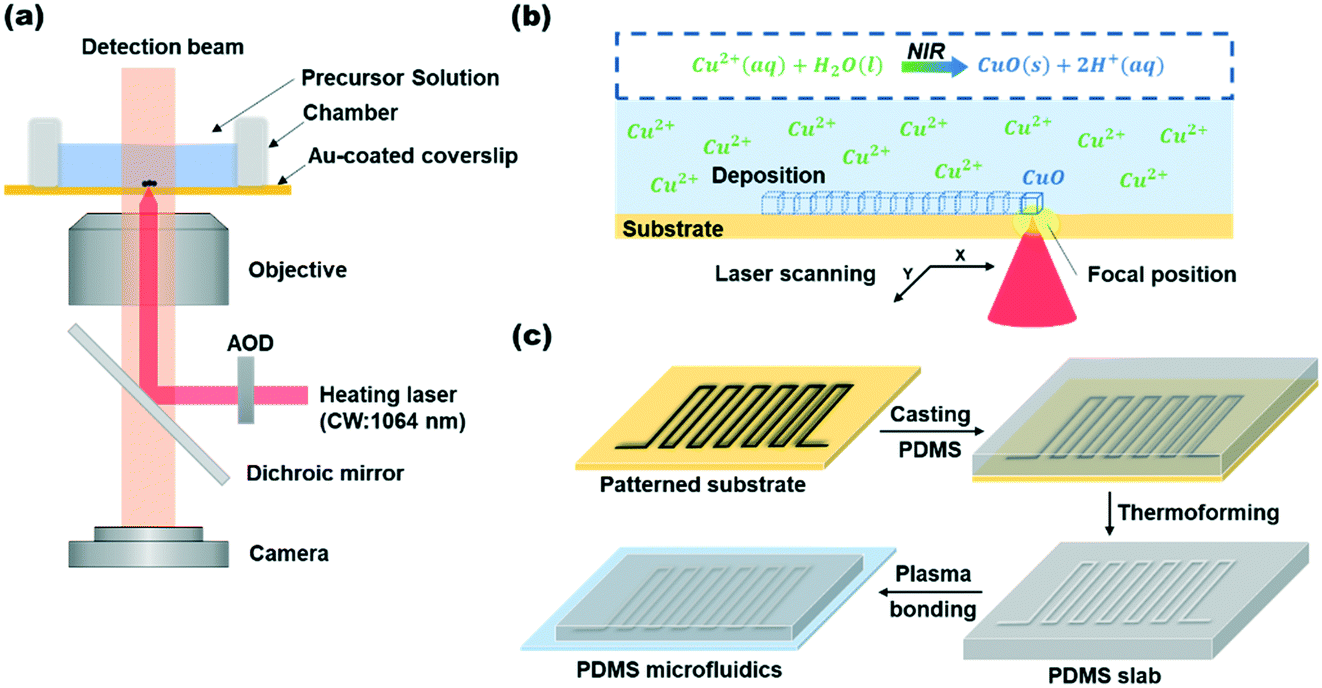 | ||
| Fig. 1 (a) Schematic configuration of the experimental setup for laser click deposition (LCD). (b) Illustration of the proposed LCD process for metal-oxide micro/nano-structure synthesis on the Au substrate. (c) Flow process for fabricating microfluidic chips using LCD method. | ||
We precisely manipulated the position and intensity of the optical trap using an acousto-optic modulator (AOD) in the optical tweezers system. The computer program controlled the spatial coordinate movement of the optical trap, resulting in the highly precise positioning of the near-infrared laser beam in two dimensions. It then enabled the deposition of microstructures on the substrate. In the experiments, we scanned the laser beam in the defined steps using the AOD with 10 nm accuracy. As illustrated in Fig. 1b, a series of spots with a specified interval on the substrate were sequentially selected along the horizontal position. By successively focusing the near-infrared laser beam on the center of each position, a dense linear structure can be formed on the substrate. On this premise, the general procedures of the LCD technique for fabricating microfluidic chips were similar to those molding methods, and the overall process was separated into four steps (Fig. 1c). To begin with, the computer software program created the desired pattern. Thus, by using the LCD technique, the patterned transition metal oxide can be directly printed on the master template made of endothermic materials. The second step was to coat the template with a mixture of polydimethylsiloxane (PDMS)37 and its corresponding cross-linking agent, which can be plasticized when heated to a high temperature. Thirdly, after the PDMS polymer material had been cured, we peeled it off from the master mold. Then, a microfluidic platform with precisely defined microstructures was obtained. Finally, a glass slide was used to bond with the microfluidic platform, yielding a sealed microfluidic chip for further uses.
To assess the quality of the master mold fabricated by the LCD technique, the surface morphology of the deposition materials was characterized by scanning electron microscopy (SEM) and atomic force microscopy (AFM). The research object discussed in Fig. 2 is CuO, which is obtained via LCD using 20 mmol L−1 Cu(Ac)2 precursor solution. Fig. 2a provides the SEM image of the deposition array. Each laser click event deposits a round CuO dot with smooth surface and sharp edge, indicating the potential of CuO materials to be used as the templates for fine microfluidic channels. Fig. S1† displays the SEM images of a single CuO dot with higher magnification. Elemental mapping using energy dispersive X-ray spectroscopy (EDS) shows that oxygen and copper element are uniformly distributed throughout the deposition material. Meanwhile, in situ Raman spectroscopy of the deposition (Fig. 2b) provides further information about its chemical composition at the micro level. The Raman spectrum shows multiple sharp peaks at 294 cm−1, 344 cm−1 and 625 cm−1, which correspond to the Ag, Bg1 and Bg2 modes of the full hydrolysate CuO, respectively.38 In addition, when comparing to the standard spectra of Cu(Ac)2 and Cu(OH)2 (Fig. 2c), one finds the absence of the characteristic peaks at 950 cm−1 and 321 cm−1 in Cu(Ac)2, and at 487 cm−1 in Cu(OH)2. In summary, under the influence of the micro-scale thermal effect, the aqueous solution of Cu(Ac)2 completely hydrolyzes into CuO.
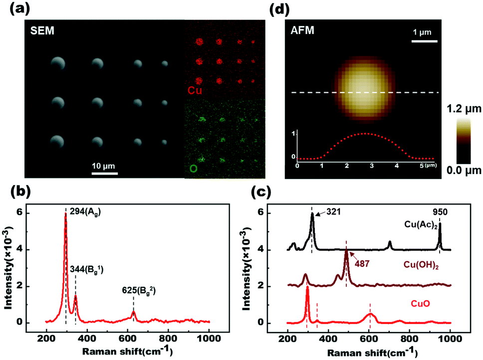 | ||
| Fig. 2 Characterization of material deposited from cupric acetate aqueous precursor. (a) SEM image of resulting deposition array obtained from LCD, and the element mapping of Cu and O. The scale bar is 10 μm. (b) Raman spectra of deposition materials on the Au substrate with Cu(Ac)2 as the precursor solution (red). The peaks at the position of the black dash line belong to Ag, Bg1, Bg2, respectively. (c) Standard Raman spectra of Cu(Ac)2 powder (i), Cu(OH)2 powder (ii) and CuO powder (iii) from bottom to up, respectively. (d) AFM image of CuO microstructure on Au substrate. Insert: Height profiles of the corresponding dash line. The scale bar is 1 μm. | ||
Interestingly, several precursors may be used to modify the chemical composition of the deposited materials throughout the LCD process (ESI,† Fig. S2). Acetate salts are employed as precursor solutions for depositing metal oxides, because they stimulate hydrolysis reactions more than other salts. For example, zinc oxide deposits directly from the zinc acetate solution. Thus, the LCD technique offers a generic path for the direct writing of various metal oxides.
The AFM image of the deposition material is shown in Fig. 2d. The microstructure is shaped like a spherical cap, with a higher altitude at the center than at the edge. It is consistent with the two-dimensional Gaussian distribution of the laser spot, in which heat distribution is concentrated toward the center of the region. This feature implies that the LCD process is influenced by the laser intensity, which will be discussed later. The beam energy at the focal spot shows a Gaussian distribution, which results in heat being accumulated at the center point and spreading to the surrounding area by a certain temperature gradient. When the temperature falls below the nucleation temperature, the hydrolysis reaction ceases, leaving a weaker degree of hydrolysis at the edges than at the center of the deposition.
Regulating and monitoring of direct laser writing system
To further understand the impact of processing parameters, we use the CuO material as an example to illustrate the relationship of the deposited particle size with the laser power and the exposure time. In this study, stable structures were generated using a continuous laser beam (λ = 1064 nm). The deposition materials were arranged in a rectangular array according to their deposition conditions. Fig. 3a shows the size of the deposition material under different exposure times, and the deposition power is kept constant at 5.9 mW. It is clear that longer exposure time results in larger particle sizes. The diameter of the deposited particle increases rapidly with time during the first 5 seconds. When the exposure time is raised to 20 seconds, the diameter tends to reach its maximum value and then changes slowly. The minimal exposure time required to build a stable structure at such laser power is 10 ms, and the spatial resolution in the horizontal plane achieved at the threshold time is 500 nm. By controlling the exposure time, we can generate the deposited particle with a diameter smaller than the laser spot (∼1 μm). This indicates that the LCD technique can achieve sub-micron spatial resolution in applications.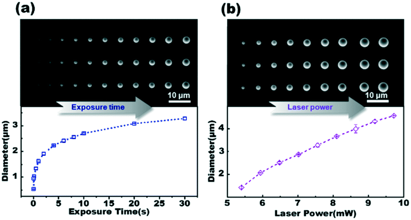 | ||
| Fig. 3 (a) Graph of grown cupric oxide micro/nano-structure diameter under various exposure times. Upper: SEM images of deposited particle array at various exposure times; Lower: the dependence of grown CuO particle diameter on exposure time. (b) Graph of grown copper oxide micro/nano-structure diameter at various laser powers. Upper: SEM images of CuO particle array at various laser powers; Lower: the dependence of grown CuO particle diameter on laser powers. The growth conditions change horizontally, while the growth conditions in each column are identical. The error bars represent the standard error range. The scale bar is 10 μm. | ||
Fig. 3b illustrates the change in particle sizes as a function of laser power, with a constant deposition time of 2 s. The diameter of the deposited particles rises linearly as the laser intensity increases. When the laser power increases to 9.7 mW, water vapor bubbles are formed at the surface of the superheated Au film.39 Consequently, the maximum diameter obtained by the LCD technique is 4.6 μm under the aforementioned condition. It's also worth mentioning that the thickness of the deposited particle is consistent with the changing trend of its diameter. The thickness of the deposited material rises in direct proportion to the lengthening of the exposure time and the increase in laser power. When the exposure time reaches a certain level, the thickness of the deposited material reaches its maximum value and remains constant (ESI,† Fig. S3 and S4).
The precise settings of exposure time and laser power are critical for depositing CuO of an expected size at the designated position. When the temperature approaches the critical point for the hydrolysis reaction, the metal cations at the focal spot begin rapidly hydrolyzing to form metal oxide materials. The range of the high temperature region is expanded as laser power increases. The size of the deposition material grows in response to a significant increase in accumulated heat. A shorter exposure time would result in insufficient heat accumulation on the Au film, leaving a smaller diameter for the deposition material. Additionally, the dot array in Fig. 3 displays the ability to edit each pixel in the pattern. Thus, we can fabricate the desired patterns on the master template by optimizing the parameters of the laser system, which will be discussed in more detail later. It is worth noting that the LCD technique has excellent repeatability. In Fig. 3, the deposited particles from each vertical column are obtained under identical conditions. For example, the average diameter of the three deposited particles in the first vertical column of Fig. 3b is 1.42 μm, with a standard deviation of 0.01 μm. The stability and controllability of the LCD method meet the requirements for high-throughput and high-precision fabrication of microfluidic chip masters.
Through real-time optical imaging of the deposition process, we can collect essential information on growth kinetics. On this basis, the experiment may then alter the laser settings in real time in response to the growth status shown by the bright field microscope. We recorded the entire LCD process using a CCD camera with a frame rate of 10 frames per second (Fig. 4a and Movie S1†). The laser is activated at a predetermined time (t = 0 s) when the metal cations have not hydrolyzed near the focal spot, and the background signal is displayed in the upper left image. When the laser irradiation lasts for 1 s, the corresponding deposition material covers the Au film, forming a perfectly circular pattern. The diameter steadily increases in bright field image once the particle is formed due to continuous heating. To extract real-time information on material growth during deposition process, we analyzed 400 sequential bright field photos. The first step is to identify the particle edge in the bright field image. We extracted the pixels along the particle edge according to the threshold and change in brightness of the particle. The second stage involves applying the least squares algorithm for circle fitting to estimate the curve parameters of the hemispherical particle,40 such as the center coordinate (x, y) and radius of the particle. On this premise, we see that the radius R of the dot-like deposition particle grows with time in the manner of power-law. This tendency is compatible with the classical growth kinetic model, which is in good agreement with the theory of Lifshitz–Slyozov–Wagner (LSW).41 It indicates that the LCD process is fundamentally a thermo-driving spontaneous process.
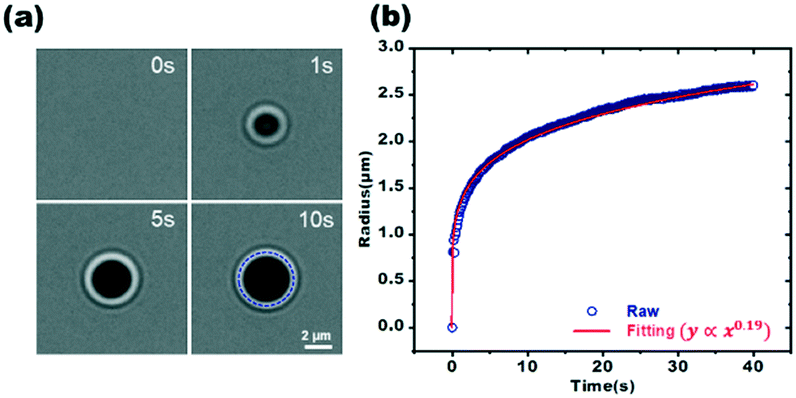 | ||
| Fig. 4 (a) In situ bright field microscope image of CuO microstructure growth at different growth time (0 s, 1 s, 5 s, 10 s). (b) The evolution of the instantaneous radius of CuO microstructure with time (blue). The particle radius is calculated according to Circle Fit. The power law fitting (red) shows the on-demand capability of tuning the patterning size using the bright field microscope. | ||
Master mold design and microfluidic chip validation
After understanding the processing parameters, we may program the scan of the laser beam to create more complex patterns. Fig. 5 shows three complex master mold patterns prepared by the LCD technique, which are then characterized by SEM. A micro-QR code with dimensions of 50 μm × 50 μm is shown in Fig. 5a. Here, we integrated the on/off state of the laser beam with its displacement to arrange a dot array in a two-dimensional plane with some regularity (Movie S2†). The pattern was formed at a laser power of 7.6 mW with an exposure time of 50 ms per position. This high-resolution miniature two-dimensional QR code can be applied in the field of microstructure anti-counterfeiting. Fig. 5b shows how the LCD technique can write line patterns directly on the substrate. The pattern was written under the setting of a laser power of 7.6 mW and a scan speed of 2 μm s−1. Each section in number 2 is approximately 10 μm in length and 1 μm in width. The lines have outstanding structure and morphology, with sharp edge at the intersections of two lines. Fig. 5c exhibits a miniature pattern of the logo of Nanjing University. As seen, the four characters are precisely designed without deformation or omission. Additionally, the morphology of the fine structures patterned by the LCD process is fairly apparent. It demonstrates that, by modifying the laser beam parameters like position and power in real time, the LCD process is capable of rapidly constructing arbitrary patterns with high spatial resolution. Along with Au film, we have observed that the laser click deposition process may be initiated on other photothermal substrates, including glass with Au film edges, ITO, and FTO conductive glass (ESI,† Fig. S5). The ability to pattern CuO microstructures on various substrates may lower the cost of manufacturing master molds of microfluidic chips via LCD.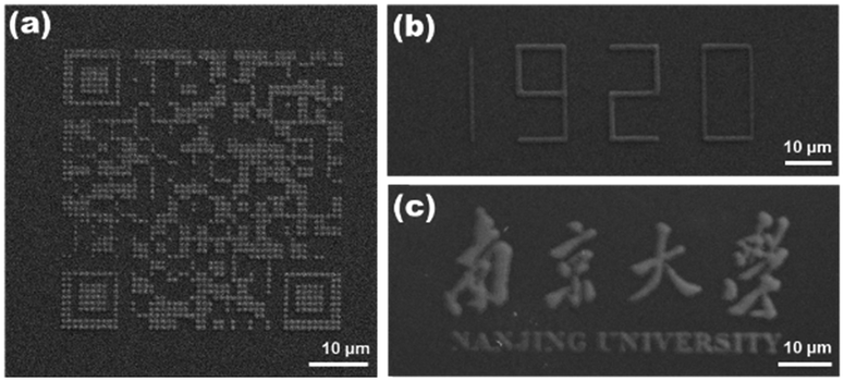 | ||
| Fig. 5 SEM images of patterned CuO structures by applying programmed LCD processes: (a) microscale 2-dimensional bar code, (b) Arabic numerals 1920, and (c) Nanjing University logo. The scale bar is 10 μm. | ||
The master mold can define multiple types of microfluidic chips. The channel structure is critical for the design of microfluidic chips. Fig. 6 shows the top views of three different microfluidic channel structures. The upper row displays the bright-field image of the master mold. The channel was then filled with Rhodamine 6G solution, which had fluorescent characteristics that allowed us to see the details of the microfluidic channel against a dark background with greater clarity under fluorescence microscope. Cross-shaped and Y-shaped junctions are the common structural patterns in microfluidic devices to complete the mixing procedure.42 The Y-channel structure is 25 μm in width, as seen in the top panel of Fig. 6a. The laser beam is now focused by a 4× objective lens, resulting in a larger size of laser spot and thus the increased width of channel. Therefore, the LCD technique can provide a larger field of effective action area while maintaining the writing speed by switching to the low magnification objective lens. It is found that the CuO structure exhibits high adherence (ESI,† Fig. S6 and S7). The key features of the channel did not deform or fall away from the substrate after 10 cycles of the cast, cure, and peel processes.
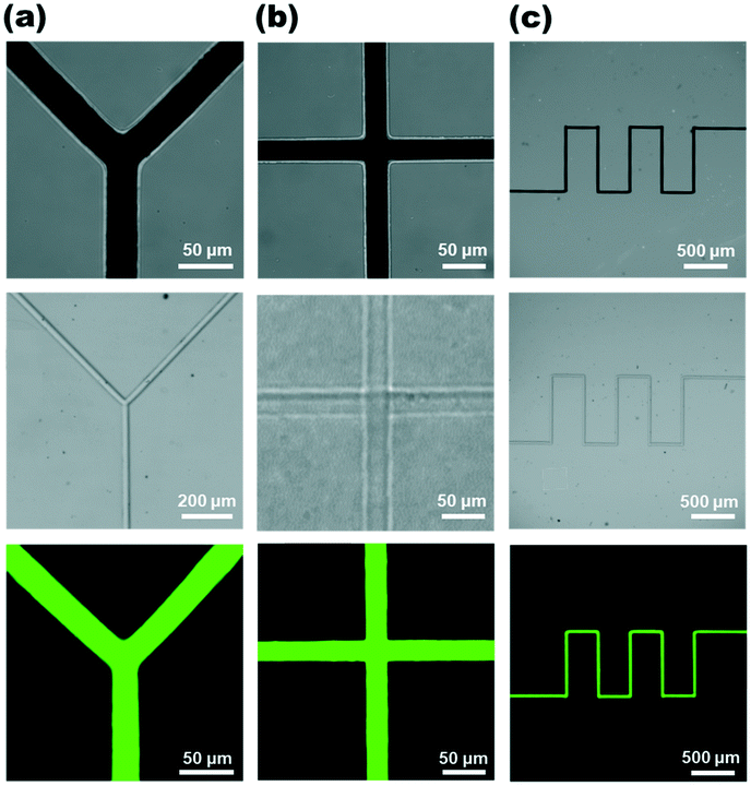 | ||
| Fig. 6 The bright field images of the master molds (upper image) and the microchannels (middle image), and the fluorescence microscope images of the microchannels filled with the solution of fluorescent rhodamine 6G (lower image). (a) Y-shaped structure. The scale bars are 50 μm, 200 μm and 50 μm, respectively. (b) Cross-shaped structure. The scale bars are 50 μm. (c) Snake-shaped structure. The scale bars are 500 μm. | ||
Furthermore, Fig. 6c displays the serpentine structure that is often used in microfluidic systems. In capillary electrophoresis-based microfluidic devices, the serpentine structure extends the length of the separation channel and hence enhances overall separation efficiency.43 The injection width of the rhodamine 6G fluorescent solution was commensurate with the channel width of the microfluidic chip, and repeated trials revealed no leakage. The microfluidic chip formed by the master mold was capable of performing the injection operation while the liquid flowed freely in the microchannel. The LCD technique, as a result, has the potential to create the master molds of microfluidic chips on a massive scale. The method allows for the manufacture of the master mold without the need for a photomask, as well as the transfer of the designed pattern without the use of photoresist as an intermediate. By directly manipulating the power and position of the laser beam, it is possible to fabricate CuO structures at any arbitrary location on the master template, allowing the pattern to be directly transferred to the microfluidic chip through the master mold.
Conclusions
In this study, we proposed a LCD technique for manufacturing master molds of microfluidic chips. This technique uses a laser beam focused on the substrate that has been covered with the transition metal salt solution, resulting in the formation of microstructures of CuO within the confined space surrounding the laser spot. Thanks to the management of the custom program over the laser beam's location, intensity, and illumination time, complex microstructures on the master template are generated with high quality. Since the size and structure of the deposition material can be adjusted by modifying the process parameters, we explored the relationship of the microstructure size with the illumination time and power of the laser beam in order to optimize the deposition process. Finally, we successfully fabricated a range of microfluidics and validated their application potential in microfluidic systems using fluorescent solution. Unlike other direct laser writing additive techniques, LCD relies on the micro-scale temperature effect to drive the hydrothermal reaction, which avoids the need for high-energy lasers and highly toxic solvents. This technique enables quick prototyping and low-cost manufacture of microfluidic chips with significant implications for applications in sensors and diagnostics.Author contributions
M. Lv performed the experiments and wrote the manuscript. M. Lv and K. Zhou designed the research and analysed the data. W. Wei and B. Niu assisted to characterize the deposition materials. X. He, H. Li, S. Liu and H. Su helped to discuss the results. W. Wang conceived and supervised this research.Conflicts of interest
There are no conflicts to declare.Acknowledgements
We thank the National Natural Science Foundation of China (Grants No. 21874070, 22004066) for financial support.References
- Y. G. Shen, Y. Yalikun and Y. Tanaka, Sens. Actuators, B, 2019, 282, 268–281 CrossRef CAS.
- H. Zhang, G. Chen, Y. Yu, J. Guo, Q. Tan and Y. Zhao, Adv. Sci., 2020, 7, 2000789 CrossRef CAS PubMed.
- S. Roy, F. Arshad, S. Eissa, M. Safavieh, S. G. Alattas, M. U. Ahmed and M. Zourob, Sens. Diagn., 2022, 1, 87–105 RSC.
- S. T. Sanjay, W. Zhou, M. Dou, H. Tavakoli, L. Ma, F. Xu and X. Li, Adv. Drug Delivery Rev., 2018, 128, 3–28 CrossRef CAS PubMed.
- J. W. Choi, Y. J. Kim, J. M. Lee, J. H. Choi, J. W. Choi and B. G. Chung, BioChip J., 2020, 14, 298–307 CrossRef CAS.
- Y. Nie, C. Jin and J. X. J. Zhang, ACS Sens., 2021, 6, 2584–2592 CrossRef CAS PubMed.
- Y. Xie, S. Yang, Z. Mao, P. Li, C. Zhao, Z. Cohick, P. H. Huang and T. J. Huang, ACS Nano, 2014, 8, 12175–12184 CrossRef CAS PubMed.
- L. Y. Sun, F. K. Bian, Y. Wang, Y. T. Wang, X. X. Zhang and Y. J. Zhao, Proc. Natl. Acad. Sci. U. S. A., 2020, 117, 4527–4532 CrossRef CAS PubMed.
- S. Zahertar, H. Torun, R. Tao, P. Canyelles-Pericas, J. Luo, Q. Wu and Y. Fu, Sens. Diagn., 2022, 1, 270–279 RSC.
- J. Baek, Y. Shen, I. Lignos, M. G. Bawendi and K. F. Jensen, Angew. Chem., 2018, 57, 10915–10918 CrossRef CAS PubMed.
- Y. Yu, J. Guo, B. Ma, D. Zhang and Y. Zhao, Sci. Bull., 2020, 65, 1752–1759 CrossRef CAS.
- C. Liu, J. Guo, F. Tian, N. Yang, F. Yan, Y. Ding, J. Wei, G. Hu, G. Nie and J. Sun, ACS Nano, 2017, 11, 6968–6976 CrossRef CAS PubMed.
- Y. Y. Hao, Y. J. Bao, X. Y. Huang, Y. J. Hu and B. Xiong, RSC Adv., 2018, 8, 39811–39817 RSC.
- H. Zhang, J. J. Wang, J. Fan and Q. Fang, Talanta, 2013, 116, 946–950 CrossRef CAS PubMed.
- C. M. Huang, Y. Zhu, D. Q. Jin, R. T. Kelly and Q. Fang, Anal. Chem., 2017, 89, 9009–9016 CrossRef CAS PubMed.
- S. R. Gao, W. T. Tung, D. S. H. Wong, L. M. Bian and A. P. Zhang, J. Micromech. Microeng., 2018, 28, 095011 CrossRef.
- P. Mali, A. Sarkar and R. Lal, Lab Chip, 2006, 6, 310–315 RSC.
- D. Huh, B. D. Matthews, A. Mammoto, M. Montoya-Zavala, H. Y. Hsin and D. E. Ingber, Science, 2010, 328, 1662–1668 CrossRef CAS PubMed.
- S. Hector and P. Mangat, J. Vac. Sci. Technol., B, 2001, 19, 2612–2616 CrossRef CAS.
- D. C. Duffy, J. C. McDonald, O. J. Schueller and G. M. Whitesides, Anal. Chem., 1998, 70, 4974–4984 CrossRef CAS PubMed.
- X. Zhang, H. T. Li, Z. X. Wang, X. Y. Chen and Q. Li, Biomed. Microdevices, 2018, 20, 1–6 CrossRef PubMed.
- J. Yeo, S. Hong, M. Wanit, H. W. Kang, D. Lee, C. P. Grigoropoulos, H. J. Sung and S. H. Ko, Adv. Funct. Mater., 2013, 23, 3316–3323 CrossRef CAS.
- T. Trantidou, M. S. Friddin, K. B. Gan, L. Y. Han, G. Bolognesi, N. J. Brooks and O. Ces, Anal. Chem., 2018, 90, 13915–13921 CrossRef CAS PubMed.
- S. S. Chou, B. S. Swartzentruber, M. T. Janish, K. C. Meyer, L. B. Biedermann, S. Okur, D. B. Burckel, C. B. Carter and B. Kaehr, J. Phys. Chem. Lett., 2016, 7, 3736–3741 CrossRef CAS PubMed.
- L. D. Zarzar, B. S. Swartzentruber, B. F. Donovan, P. E. Hopkins and B. Kaehr, ACS Appl. Mater. Interfaces, 2016, 8, 21134–21139 CrossRef CAS PubMed.
- B. B. Xu, Y. L. Zhang, H. Xia, W. F. Dong, H. Ding and H. B. Sun, Lab Chip, 2013, 13, 1677–1690 RSC.
- T. F. Hong, W. J. Ju, M. C. Wu, C. H. Tai, C. H. Tsai and L. M. Fu, Microfluid. Nanofluid., 2010, 9, 1125–1133 CrossRef CAS.
- L. M. Wang, R. Kodzius, X. Yi, S. B. Li, Y. S. Hui and W. J. Wen, Sens. Actuators, B, 2012, 168, 214–222 CrossRef CAS.
- G. Kumi, C. O. Yanez, K. D. Belfield and J. T. Fourkas, Lab Chip, 2010, 10, 1057–1060 RSC.
- A. Singh, G. Scotti, T. Sikanen, V. Jokinen and S. Franssila, Micromachines, 2014, 5, 472–485 CrossRef.
- Z. Liu, W. Xu, Z. Hou and Z. Wu, Micromachines, 2016, 7, 201 CrossRef PubMed.
- C. N. LaFratta, O. Simoska, I. Pelse, S. Weng and M. Ingram, Microfluid. Nanofluid., 2015, 19, 419–426 CrossRef CAS.
- J. Yeo, S. Hong, G. Kim, H. Lee, Y. D. Suh, I. Park, C. P. Grigoropoulos and S. H. Ko, ACS Nano, 2015, 9, 6059–6068 CrossRef CAS PubMed.
- S. Fujii, R. Fukano, Y. Hayami, H. Ozawa, E. Muneyuki, N. Kitamura and M. A. Haga, ACS Appl. Mater. Interfaces, 2017, 9, 8413–8419 CrossRef CAS PubMed.
- K. J. Laidler, J. Chem. Educ., 1984, 61, 494–498 CrossRef CAS.
- J. Kwon, S. Hong, G. Kim, Y. D. Suh, H. Lee, S. Y. Choo, D. Lee, H. Kong, J. Yeo and S. H. Ko, Appl. Surf. Sci., 2018, 447, 1–7 CrossRef CAS.
- M. P. Wolf, G. B. Salieb-Beugelaar and P. Hunziker, Prog. Polym. Sci., 2018, 83, 97–134 CrossRef CAS.
- Y. Deng, A. D. Handoko, Y. Du, S. Xi and B. S. Yeo, ACS Catal., 2016, 6, 2473–2481 CrossRef CAS.
- J. Chen, K. Zhou, Y. J. Wang, J. Gao, T. L. Yuan, J. Pang, S. Tang, H. Y. Chen and W. Wang, Proc. Natl. Acad. Sci. U. S. A., 2019, 116, 12678–12683 CrossRef CAS PubMed.
- T. Lu, X. Deng, X. Chang and X. Liu, Science of Surveying and Mapping, 2019, 44, 33–37 Search PubMed.
- T. J. Woehl, J. E. Evans, I. Arslan, W. D. Ristenpart and N. D. Browning, ACS Nano, 2012, 6, 8599–8610 CrossRef CAS PubMed.
- F. Y. Ushikubo, F. S. Birribilli, D. R. B. Oliveira and R. L. Cunha, Microfluid. Nanofluid., 2014, 17, 711–720 CrossRef CAS.
- D. Cai, Q. Yi, C. Shen, Y. Lan, G. Urban and W. Du, Biomicrofluidics, 2018, 12, 014109 CrossRef PubMed.
Footnote |
| † Electronic supplementary information (ESI) available: Characterization of the deposition materials, the influence of the precursor solution on the composition of the deposited materials, the dependence of the deposition thickness on laser parameters, the feasibility of constructing the laser click deposition process on various substrates, bright field microscope image of the designated pattern and its corresponding microchannel, and description of movies. See DOI: https://doi.org/10.1039/d2sd00060a |
| This journal is © The Royal Society of Chemistry 2022 |