
 Open Access Article
 This Open Access Article is licensed under a Creative Commons Attribution-Non Commercial 3.0 Unported Licence
The holy grail of pyrene-based surface ligands on the sensitivity of graphene-based field effect transistors
Vladyslav
Mishyn†
a,
Adrien
Hugo†
 a,
Teresa
Rodrigues
b,
Patrik
Aspermair
b,
Henri
Happy
a,
Leonel
Marques
c,
Charlotte
Hurot
c,
Riadh
Othmen
c,
Vincent
Bouchiat
c,
Rabah
Boukherroub
a,
Wolfgang
Knoll
bd and
Sabine
Szunerits
*a
a,
Teresa
Rodrigues
b,
Patrik
Aspermair
b,
Henri
Happy
a,
Leonel
Marques
c,
Charlotte
Hurot
c,
Riadh
Othmen
c,
Vincent
Bouchiat
c,
Rabah
Boukherroub
a,
Wolfgang
Knoll
bd and
Sabine
Szunerits
*a
aUniv. Lille, CNRS, Centrale Lille, Univ. Polytechnique Hauts-de-France, UMR 8520 – IEMN, F-59000 Lille, France. E-mail: sabine.szunerits@univ-lille.fr
bAIT Austrian Institute of Technology GmbH, Biosensor Technologies, 3430 Tulln, Austria
cGRAPHEAL SAS, 25 avenue des Martyrs, 38042 Grenoble CEDEX 09, France
dDepartment of Scientific Coordination and Management, Danube Private University, A-3500 Krems, Austria
First published on 5th January 2022
Abstract
Graphene has received intensive research interest due to its remarkable charge mobility, and the efforts in the use of graphene-based field effect transistors (GFETs) for the sensing of biological biomarkers is on the rise. Because of the high non-specific protein adsorption on graphene, well-defined surface modification strategies have to be implemented to benefit from the excellent electronic transfer characteristics of GFET devices for specific detection of biomarkers. Surprisingly, while pyrene-based ligands are the most widely used graphene surface anchors for sensing-related applications, no systematic investigation on the reaction conditions employed and the influence of pyrene functionalities has been reported so far. As this is one of the essential steps for efficient receptor integration and sensitive sensing, by using GFET-based analysis of cardiac troponin I (cTnI) as the model compound we will show that an optimized pyrene–maleimide ligand incubation time on graphene of 2 h gives the best sensing performance. This study not only will be a guideline for researchers interested in GFET biosensors but also will hopefully allow industrial GFET development in a faster path.
Introduction
In the past years, we have witnessed an overwhelming research interest in graphene.1–5 To fully harness the potential of graphene for sensing-related applications and allow a controlled tuning of its physical and chemical properties, surface functionalization became an important topic in graphene research.6–10 While covalent functionalization has become by far the most promising approach for reaching robust and stable interfaces,7,11–13 this strategy causes the most significant change in the electric band structure of graphene due to the rehybridization of sp2 carbons to sp3 carbons not only on graphene edges but also on the basal plane of a graphene lattice. This has promoted the use of non-covalent modifications mostly relying on π–π stacking interactions of aromatic ligands with graphene, with an obvious benefit of retaining the structures and electrical properties of graphene with this approach.11,14 Pyrene-based surface ligands have been most widely employed, as van der Waals forces between graphene and the pyrene backbone ensure their tight binding via π stacking.14–19 For receptor-based analyte sensing, anchoring surface ligands to a graphene channel is an important part of designing a functional GFET biosensor. Pyrene-modified nitriloacetic acid was proposed, for example by Singh et al., to further attach biotinylated cholera toxin via biotin–copper coordination.16 Ingrosso et al. used 1-pyrenebutyric acid (PBA) to anchor PbS nanocrystals to graphene sheets.20 Our group used PBA for the covalent grafting of an aptamer specific to the human papillomavirus HPV-16 E7 protein.15 Poly(ethylene glycol) modified pyrene (pyrene-PEG) was used for inhibiting the surface fouling of reduced graphene oxide matrices and for a selective isolation of E. coli associated with urinary tract infections,21 or electrochemical sensing of cardiac troponin I.22 The use of 1-pyrenebutanoic acid succinimidyl ester (PBASE) became particularly popular for non-covalent modification of graphene.1,23–25 As a heterobifunctional linker, it contains a pyrene group that stacks onto graphene by π–π overlapping and an N-hydroxysuccinimide (NHS) ester that reacts with primary amines. As has been lately stated by Wang et al., the conditions used for modification of graphene with PBASE are crucial in maximizing the device performance.1 They optimized this process by incubating graphene in dry dimethylformamide (DMF) solutions of 50 mM PBASE for 1–8 h at room temperature. A time of 4 h was identified as optimal, as longer times resulted in aggregation of pyrene groups onto monolayer graphene forming a structure similar to that of bilayer graphene.In spite of the importance of PBASE, the question of knowing if PBASE is the most suitable surface ligand for obtaining optimal receptor integration via post-functionalization can be raised due to the labile character of the reactive ester function. How does PBASE integration onto graphene compare to other pyrene-based surface ligands such as 1-pyrenebutyric acid (PBA) or a pyrene–maleimide linker, where the maleimide unit is separated from the pyrene unit by 7-carbon units and the bulk cyclic maleimide tail is orientated perpendicular to pyrene? Thodkar et al. have investigated self-assembled pyrene stacks and their influence on electrolyte-gated GFET transistors lately.19 Their data suggests that when incubating for 1.5 h in a mixture of PBA/pyrene–maleimide (1 mM/0.5 mM) in DMF, a right shift of the Dirac point is observed with a decrease of charge mobility by 5% due to the formation of dense, ordered multilayers on graphene as evidenced by AFM. For the use of GFETs as biosensors, next to understanding how pyrene stacks on graphene, the ultimate integration of a controlled amount of a bioreceptor is required. How will different pyrene derivatives and interaction times with graphene influence the final grafting density and sensor performance?
Table 1 highlights different GFET biosensors where various aromatic surface linkers were employed for receptor integration. The key advantages of using the π–π stacking interaction capability of aromatic ligands with graphene for introducing surface functions are that they do not alter the graphene band structure, conserve the initial electronic properties and show a binding energy of EB = −48 meV per C strong enough to link a bioreceptor and perform sensing. The group of Chappell et al. has demonstrated using DFT calculations that the binding energy for benzene, naphthalene, anthracene and pyrene increases with the increase in the C/H ratio making the pyrene-based molecules the top performer in the row.26 Interestingly, substituents in the aromatic molecules enhance the binding to graphene due to secondary attractive interactions with graphene. Compared to other non-covalent bioprobes (e.g. BSA,27 Au NPs,28 polymers29etc.), pyrene-based ligands are small in size and are attached in close vicinity to the graphene interface. This is especially important for electrical biosensors, since the ionic strength of the solution greatly reduces the Debye sensing range and makes these sensors sensitive only in the immediate vicinity of the graphene surface.30
| Target analyte | Electrode architecture | Surface chemistry | Probe | Ref. |
|---|---|---|---|---|
| G: graphene; BSA: bovine serum albumin; Ab: antibody; DNA: deoxyribonucleic acid; GOD: glucose oxidase; JR2EC: de novo designed synthetic polypeptide for MMP-7. | ||||
| SARS-CoV-2 | G/PBASE-Ab | π–π stacking | PBASE | 31 |
| E. coli bacteria | G/PBASE-Ab | π–π stacking | PBASE | 32 |
| Papillomavirus | G/PBA-aptamer | π–π stacking | PBA | 15 |
| Glucose | G/PBA-GOD | π–π stacking | PBA | 33 |
| T4 lysozyme | G/PMAL | π–π stacking | PMAL | 34 |
| Matrilysin MMP-7 | G/PMAL-JR2EC | π–π stacking | PMAL | 35 |
To shed more light on this apparently trivial reaction, three different pyrene ligands were integrated for different time intervals onto the graphene-based interfaces (Fig. 1) in this work. Using Raman spectroscopy and cyclic voltammetry (CV), the impact of the incubation time (2 h to 24 h) for each linker on the final graphene–pyrene interface was probed, and a surface coverage value was obtained using a ferrocene redox probe covalently attached to each linker. Our results show the benefits of using pyrene-propanoic amid ethylmaleimide (PMAL) and how tailoring incubation conditions is crucial to promote an optimal GFET sensing response using cardiac troponin I (cTnI) protein as a model analyte for sensing.
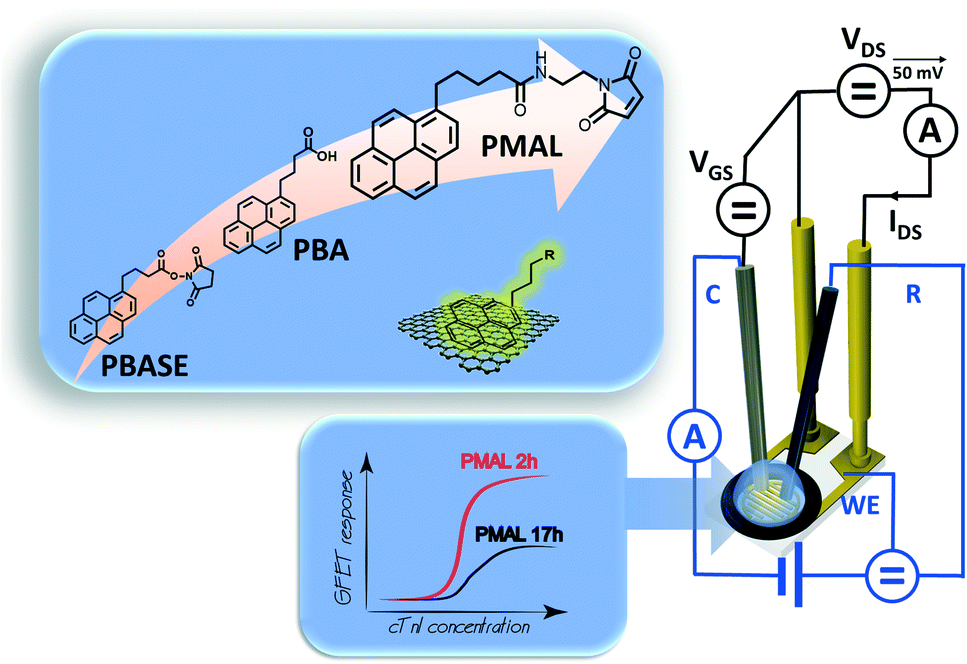 | ||
| Fig. 1 Liquid gated graphene-based field effect transistor combined with a classical three-electrode electrochemical setup. The graphene surface is modified with three different pyrene ligands. | ||
Results and discussion
Graphene modification with 1-pyrenebutanoic acid succinimidyl ester (PBASE)
1-Pyrenebutanoic acid succinimidyl ester (PBASE) is the most widely used pyrene-based graphene anchor as it allows the linking of molecules containing lysine and NH2 residues readily via the formation of amide bonds. The graphene-based interfaces used in this study are interdigitated gold electrode (IDE) arrays of 90 pairs, each with a width of 10 μm, and separated by 10 μm as used earlier by us,15 with the main difference in the channel material, in which CVD grown graphene was used instead of reduced graphene oxide (Fig. 1).36 The Raman spectra recorded after wet-chemical transfer of graphene on different areas of the device underline the homogenous character of the interface (Fig. 2a) with a dominating band at 1580 cm−1 assigned to the G band of graphene sp2 carbon lattice and contributions at 1350 cm−1 (D band), 2706 cm−1 (2D secondary D band) and ∼2450 cm−1 (low-intensity D + D′′ contribution) due to defects in the graphene sheet introduced during the transfer. The intensity ratios I2D/IG = 2.04 ± 0.07 and ID/IG = 0.35 indicate a high-quality graphene monolayer with low disorder.37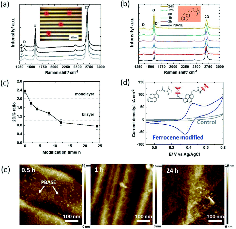 | ||
| Fig. 2 1-Pyrenebutanoic acid succinimidyl ester (PBASE) modified GFET devices: (a) Raman spectra at different areas of the initial GFET interface after wet-chemical transfer of graphene onto the IDE (inset: optical image of the GFET device and the spots where the Raman spectra were taken). (b) Raman spectra recorded at different time intervals (0, 2, 4, 8, 12 & 24 h) upon immersion of the GFET device into PBASE (5 mM, DMF). (c) I2D/IG ratio extracted from Fig. 2b. (d) Cyclic voltammograms of the ferrocene modified GFET (4 h) in acetonitrile/NBu4PF6 (0.1 M) (blue) and the unmodified GFET interface immersed in ferrocene-NH2 (control; grey), scan rate = 100 mV s−1 (inset: interaction of PBASE with ferrocene-NH2). (e) AFM images of the GFETs having been immersed for 0.5, 1 and 24 h into PBASE (5 mM) solutions. | ||
The recorded Raman spectra of graphene coated interdigitated electrodes when immersed in PBASE (5 mM) for increasing times (up to 24 h) (Fig. 2b) show the appearance of a defect induced D′ band at 1620 cm−2 after 2 h immersion, with its intensity increasing with time. The mechanism giving rise to the D′ band is due to the interaction of the localized vibration modes of PBASE with the extended phonon modes of graphene.1 The I2D/IG ratio (Fig. 2c) gradually decreases to an I2D/IG value <2 after 2 h modification, and approaches 1 after 6 h of PBASE/graphene interactions. The decrease of the I2D/IG ratio is related to multilayer formation on graphene, with an I2D/IG ratio equal to 1 for bilayer graphene.37 For incubation time longer than 12 h, aggregation of pyrene groups has therefore taken place onto the monolayer graphene sheets, structurally similar to bilayer graphene. To reach a sufficient coverage while limiting the introduction of defects, an optimal modification time would be below the 6 h time span using 5 mM PBASE in DMF.
To estimate the amount of receptor ligands which can be integrated into the PBASE modified GFET at different incubation times, post-treatment of the ester groups with ferrocene-amide was performed readily after (inset in Fig. 2d). From the cyclic voltammogram of the ferrocene modified GFET (Fig. 2d) the amount of surface linked ferrocene was evaluated using eqn (1)
| Γ = Q/nFA | (1) |
| Time [h] | Γ [mol cm−2] | |
|---|---|---|
| a Non-specific interaction as deduced from Fig. 2d: Γ = 1.81 ± 0.35 × 10⁻¹¹ mol cm−2. b Non-specific interaction as deduced from Fig. 3d: Γ = 1.84 ± 0.87 × 10⁻¹¹ mol cm−2. c Non-specific interaction as deduced from Fig. 4d: Γ = 3.07 ± 0.37 × 10⁻¹¹ mol cm−2. | ||
| PBASEa | 2 | 6.04 ± 1.01 × 10⁻¹¹ |
| 4 | 6.44 ± 1.52 × 10⁻¹¹ | |
| 6 | 8.02 ± 2.36 × 10⁻¹³ | |
| 12 | 0 | |
| 24 | 0 | |
| PBAb | 2 | 4.14 ± 0.34 × 10⁻¹⁰ |
| 4 | 4.11 ± 0.52 × 10⁻¹⁰ | |
| 6 | 4.13 ± 0.37 × 10⁻¹⁰ | |
| 12 | 4.17 ± 0.29 × 10⁻¹⁰ | |
| 24 | 4.17 ± 0.51 × 10⁻¹⁰ | |
| PMALc | 2 | 4.18 ± 0.25 × 10⁻¹⁰ |
| 4 | 3.96 ± 0.18 × 10⁻¹⁰ | |
| 6 | 1.77 ± 0.28 × 10⁻¹⁰ | |
| 12 | 1.13 ± 0.48 × 10⁻¹⁰ | |
| 24 | 1.11 ± 0.33 × 10⁻¹⁰ | |
Considering the maximum possible surface coverage density of PBASE as Γ = 4.76 × 10⁻¹⁰ mol cm−2,18 the surface coverage of ferrocene (Table 2) is less than a quarter after 2–4 h and only a fraction after 6 h. Only a small portion of the ester groups of PBASE seems to have reacted with the ferrocene ligand. The use of longer interaction times might also result in hydrolysation of the labile ester functions. The limited accessibility of the ester function is most likely not the reason for these findings. The water contact angle measurements before and after PBASE modification indicate a decrease in the water contact angle by 29% from 85 ± 1° to 60 ± 2°. The graphene surface without PBASE is largely hydrophobic, while PBASE modified graphene is hydrophilic if the ester groups are facing out of the surface.17 From the AFM images of PBASE modified GFETs for increased time spans (Fig. 2e), the PBASE deposits which formed a dense pyrene layer after 2 h are clearly visible. The labile character of the ester groups is clearly the reason for the lower grafting density of ferrocene molecules at long immersion times rather than the presence of poor pyrene stacks.
Graphene modification with 1-pyrenebutyric acid (PBA)
To study the hydrolysis of the ester functions in PBASE over time, the graphene channel was further modified with 1-pyrenebutyric acid (PBA) for 2–24 h in the same manner as that with PBASE (Fig. 3a). Similar to the trend observed for the PBASE linker, the I2D/IG ratio (Fig. 3b) decreases below 2 after 2 h modification, eventually reaching a value below 1 after 24 h of modification, suggesting a similar non-specific pyrene multilayer formation when increasing the incubation time.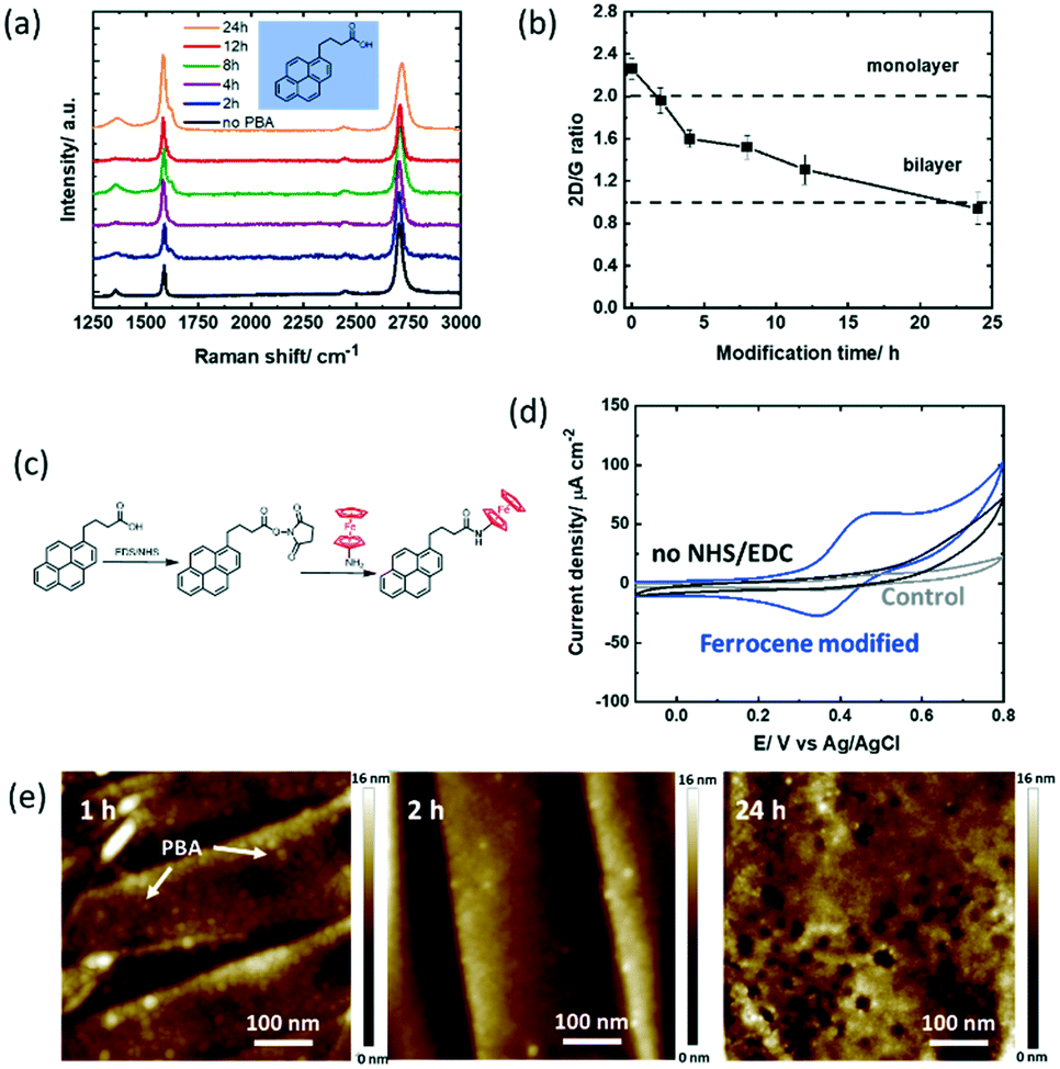 | ||
| Fig. 3 1-Pyrenebutyric acid (PBA) modified GFET devices: (a) Raman spectra recorded at different time intervals (0, 2, 4, 8, 12 & 24 h) upon immersion of the GFET device into PBA (5 mM, DMF). (b) I2D/IG ratio extracted from Fig. 3a. (c) Interaction scheme with ferrocene-NH2 utilizing NHS/EDC activation of carboxyl groups. (d) Cyclic voltammograms of the GFET modified with PBA for 4 h and post-modified with ferrocene-NH2 through NHS/EDC activation, solvent: acetonitrile/NBu4PF6 (0.1 M) (blue), the PBA modified interface immersed in ferrocene-NH2 without NHS/EDC activation, (control 2; black) and the unmodified GFET interface immersed in ferrocene-NH2 (control 1; grey), scan rate = 100 mV s−1. (e) AFM images of the GFETs modified for 1, 2 and 24 h with PBA. | ||
The surface coverage of ferrocene largely increased to Γ = 4.14 ± 0.34 × 10⁻¹⁰ mol cm−2 in 2 h, reaching 4.17 ± 0.51 × 10⁻¹⁰ mol cm−2 after 12 h (Table 2). In a first control experiment to see non-specific interaction phenomena, the unmodified GFET device was incubated in the ferrocene-NH2 redox probe. From Fig. 3d (grey curve), a surface coverage of Γ = 1.78 × 10⁻¹¹ mol cm−2 is extracted, corresponding to 3% of the maximum coverage. The noise resulting from the eventual non-specific adsorption of the redox probe directly on graphene is therefore not significant in our experiments. In a second control experiment, the GFET device modified with PBA for 4 h was immersed in ferrocene-NH2 without NHS/EDC activation (Fig. 3d). No ferrocene bound molecules were observed, similar to the those for 12–24 h of PBASE incubation. This result suggests that the low coverage ferrocene on the PBASE-modified devices is indeed due to the hydrolysis of the NHS-ester group.
In addition, the AFM images were acquired at 1 h, 2 h and 24 h (Fig. 3e). Compared to PBASE, PBA is following a faster reaction kinetic with pyrene stacks clearly observed after 1 h. However, PBA pyramids (local PBA stacking) rather than complete GFET coverage is observed at longer times. Some graphene remains uncovered with pyrene ligands in this case. For sensing based applications this will lead to increased surface fouling, which has to be avoided.
Graphene modification with pyrene-propanoic amid ethylmaleimide (PMAL)
We were intrigued to understand how a different hetero-bifunctional linker such as pyrene-propanoic amid ethylmaleimide (PMAL) would behave when in contact with a GFET device. The interest in PMAL is because cysteine and thiol carrying receptors can be readily attached to graphene using thiol–maleimide linkage via the PMAL linker. Different to PBASE (Fig. 2a), modification of the GFET with PMAL for longer than 12 h gives rise to increased D′ band contributions (Fig. 4a). Bilayer formation with I2D/IG = 1 is reached after 12 h modification (Fig. 4b).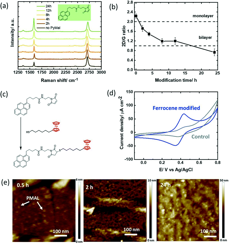 | ||
| Fig. 4 Pyrene-propanoic amid ethylmaleimide (PMAL) modified GFET devices: (a) Raman images recorded at different time intervals upon immersion of the GFET device into PMAL (5 mM, DMF). (b) I2D/IG ratio extracted from Fig. 4a. (c) Interaction scheme with ferrocene–thiol. (d) Cyclic voltammograms of the ferrocene modified GFET (4 h) in acetonitrile/NBu4PF6 (0.1 M), scan rate = 100 mV s−1 (blue) and the GFET interface immersed with ferrocene–thiol without PMAL (control; grey). (e) AFM images of GFET modified for 0.5, 2 and 24 h with PMAL. | ||
Chemical linkage of the thiolated ferrocene derivative (Fig. 4c) followed by electrochemical investigation reveals a ferrocene coverage as high as Γ = 4.18 ± 0.25 × 10⁻¹⁰ mol cm−2 after only 2 h (Table 2). Similar to PBA, the non-specific adsorption of ferrocene on graphene was not significant in our experiments (Fig. 4d). While longer incubation times yielded higher surface coverage with PBA, longer PMAL incubation times did not show increased ferrocene loading. From the AFM investigations, the formation of nm-thick PMAL films is clearly identified when the GFET surfaces are immersed overnight (Fig. 4e). The thicker film can partially block electron transfer resulting in lower ferrocene redox current. It could be also hypothesized that ferrocene is only grafted to the poorly bound upper pyrene layer being washed out during the chemical coupling process. Indeed, the bulky cyclic maleimide tail of PMAL is orientated perpendicular to pyrene and weakens pyrene–graphene π–π stacking,19 reducing the stability of multi-layered PMAL stacks. Increasing incubation times could therefore induce weaker van der Waals interactions with the substrate surface, resulting in a decrease in the ferrocene surface coverage.
Comparing PBASE, PBA and PMAL proves that PMAL is the most promising linker for further graphene functionalization. Indeed, the widely used PBASE linker suffers from hydrolysis of its ester function over time, resulting in a lower density of active moieties available for receptor grafting. PBA shows a high surface coverage but tends to form pyrene-stacks rather than fully covered GFET surfaces. This will negatively influence GFET measurements, but will also pose sensing related limitations due to increased non-specific adsorption occurring on non-modified graphene areas. It furthermore requires an additional EDC/NHS activation step to obtain a surface coverage comparable to the one obtained after 2 h of PMAL incubation.
Graphene modification with PMAL for sensing of cTnI
To validate the importance of the pyrene immersion time on GFET devices for sensing related aspects, cardiac troponin I (cTnI) was chosen as a model biomarker. This was motivated by the fact that cardiovascular diseases have become the first cause of death globally, taking an estimated 17.9 million lives each year. As the level of cTnI is directly correlated with the occurrence of acute myocardial infarction (AMI), the most life-threatening version of acute coronary syndrome causing severe irreversible tissue injury in the myocardium, it has become the golden standard for myocardial infarction diagnostics.38,39 The cut-off level of cTnI in plasma for healthy patients is currently set to 26 pg mL−1,40 two to three orders of magnitudes differentiated from the cTnI level in patients diagnosed with AMI, with serum levels of cTnI of 5000–50![[thin space (1/6-em)]](https://www.rsc.org/images/entities/char_2009.gif) 000 pg mL−1. A cTnI GFET biosensor was built by integrating a cTnI specific thiol-terminated aptamer (5′-thiol TTT TTT CGT GCA GTA CGC CAA CCT TTC TCA TGC GCT GCC CCT CTT A-3)22 through first reduction of the eventual disulphide bonds formed in the thiol-labelled aptamer, followed by covalent aptamer attachment to PMAL via formation of the maleimide–thiol bond. To insure an acceptable anti-fouling behaviour, next to the thiolated aptamer ligand, a thiol-(PEG)4-methyl was used with an aptamer/PEG ratio of 2:1 (Fig. 5a). Starting with the optimal PMAL incubation time (i.e., 2 h for a maximal PMAL surface coverage, see Table 2), the GFET transfer characteristics (IDS/VGS) were recorded in buffer (0.01× PBS/1 mM MgCl2) at each step of the device functionalization, as shown in Fig. 5b. Typically, the charge carrier density of the graphene FET channel is modulated when sweeping the potential at the gate electrode immersed in the electrolyte, with holes being the dominant charge carriers at low gate voltage (left side, p branch) and electrons at high gate voltage (right side, n branch). The two branches are separated by the so-called Dirac point (VDirac), corresponding to the potential of minimal conductivity (or the charge neutrality point), allowing the monitoring of any doping effects of graphene by its chemical environment. The GFET gating mechanism relies on the electrostatic monitoring of any charge distribution modification at the graphene–electrolyte interface (induced here by the immobilization of the pyrene linker and the aptamer receptor and the specific binding of the target analyte to the aptamer) as it is capacitively compensated by a charge carrier modulation in graphene, thus shifting the Dirac point.
000 pg mL−1. A cTnI GFET biosensor was built by integrating a cTnI specific thiol-terminated aptamer (5′-thiol TTT TTT CGT GCA GTA CGC CAA CCT TTC TCA TGC GCT GCC CCT CTT A-3)22 through first reduction of the eventual disulphide bonds formed in the thiol-labelled aptamer, followed by covalent aptamer attachment to PMAL via formation of the maleimide–thiol bond. To insure an acceptable anti-fouling behaviour, next to the thiolated aptamer ligand, a thiol-(PEG)4-methyl was used with an aptamer/PEG ratio of 2:1 (Fig. 5a). Starting with the optimal PMAL incubation time (i.e., 2 h for a maximal PMAL surface coverage, see Table 2), the GFET transfer characteristics (IDS/VGS) were recorded in buffer (0.01× PBS/1 mM MgCl2) at each step of the device functionalization, as shown in Fig. 5b. Typically, the charge carrier density of the graphene FET channel is modulated when sweeping the potential at the gate electrode immersed in the electrolyte, with holes being the dominant charge carriers at low gate voltage (left side, p branch) and electrons at high gate voltage (right side, n branch). The two branches are separated by the so-called Dirac point (VDirac), corresponding to the potential of minimal conductivity (or the charge neutrality point), allowing the monitoring of any doping effects of graphene by its chemical environment. The GFET gating mechanism relies on the electrostatic monitoring of any charge distribution modification at the graphene–electrolyte interface (induced here by the immobilization of the pyrene linker and the aptamer receptor and the specific binding of the target analyte to the aptamer) as it is capacitively compensated by a charge carrier modulation in graphene, thus shifting the Dirac point.
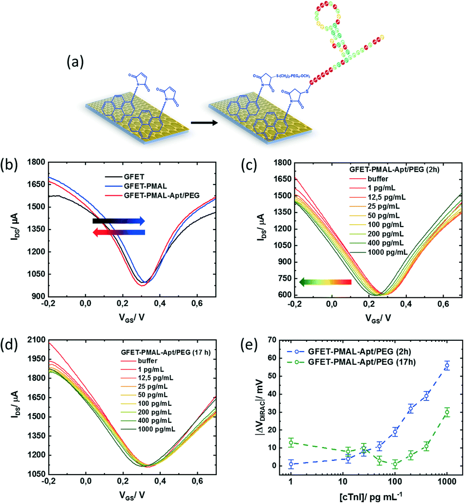 | ||
| Fig. 5 Aptamer modified GFETs for cTnI sensing and PMAL incubation time effect on the sensor performance: (a) schematic of integration of the cTnI aptamer onto the GFET. (b) Transfer characteristics of GFET, GFET-PMAL (2 h PMAL incubation) and GFET-aptamer/PEG in 0.01× PBS/MgCl2 (1 mM) (pH 7.4), applied VDS = 50 mV. (c) Transfer characteristics of the GFET devices modified with PMAL for 2 h and (d) 17 h, after stabilization for each cTnI concentration in 0.01× PBS/MgCl2 (1 mM) (pH 7.4) without washing steps, applied VDS = 50 mV. (e) Absolute Dirac point variations (ΔVDirac = VDirac ([cTnI]) − VDirac (buffer)) as a function of cTnI concentration using a logarithmic scale. | ||
Particularly, a positive VDirac (+0.31 V) is observed before GFET functionalization (Fig. 5b, black curve), which is commonly attributed to graphene p-doping induced by the fabrication process.41 After immobilization of the PMAL linker at the graphene surface (Fig. 5b, blue curve), VDirac shifts toward a more positive gate voltage (+0.33 V). As it has been consistently reported that PBASE adsorption on graphene induces hole doping due to the presence of an NHS electron withdrawer group,42–45 it is expected from PMAL molecules carrying a similar chemical functionality to also induce a hole doping effect after immobilization on graphene. Successively, a negative shift of VDirac (+0.31 V) is observed after covalent grafting of the thiolated cTnI–aptamer and PEG to PMAL linkers (Fig. 5b, red curve). Following the introduction at the graphene–electrolyte interface of the DNA aptamer made of a negatively charged phosphate backbone, one would expect positive charges to be electrostatically induced in graphene in order to insure the system charge neutrality.46 Usually, such electrostatic doping would shift VDirac toward more positive gate voltage.47 In fact, several groups have a similar reported negative VDirac shift upon DNA aptamer immobilization on graphene,48–51 which is attributed to a competitive n-doping effect induced through the interaction between the aptamer nucleoside groups and graphene.52
The PMAL–aptamer functionalized GFET sensing principle is based on conformational changes of the aptamer loop upon cTnI target binding. A current decrease is indicative of aptamer reorientation towards the sensing channel, while a current increase often indicates aptamer loop bending away from the surface.59 The transfer characteristics of the aptamer/PEG modified GFET during exposure to increasing cTnI concentrations from 1 to 1000 pg mL−1 in 0.01× PBS/1 mM MgCl2 buffer were recorded after flowing the cTnI solutions for 15 min for each concentration (Fig. 5c). A sharp Dirac point shift (ΔVDirac = VDirac ([cTnI]) − VDirac (buffer)) towards a negative gate voltage can be observed with increasing cTnI concentrations (Fig. 5e, blue curve). The predominant horizontal shift of the curves suggests that the capacitive effects are mainly at play during the whole experiment. This result agrees with the positively charged cTnI target (pI = 9.87) binding to the aptamer within the electrochemical double layer at the sensor surface, consequently inducing graphene n-doping through electrostatic gating.
With a view to show how the optimization of the density of active functionality through PMAL incubation time can affect the biosensor final performance, a GFET device was functionalized with PMAL overnight (17 h). Under these conditions, the PMAL layer at the graphene surface shows a proportion of active MAL moieties available for binding the aptamer receptor, reduced by 70% relatively to the surface coverage obtained after 2 h of PMAL incubation time (Table 2). The resulting transfer characteristics upon exposure of the sensor to increasing cTnI concentrations are shown in Fig. 5d and e (green curve). A significant negative shift of VDirac (−13 mV) is observed in response to the first cTnI concentration of 1 pg mL−1. With increasing cTnI concentrations up to 100 pg mL−1, VDirac is shifting back to the level observed in pure buffer before shifting again toward a negative voltage in the 100–1000 pg mL−1 concentration range. From this dose response curve, two graphene doping regimes can be distinguished: before (p-doping) and after (n-doping) 100 pg mL−1 analyte addition. The p-doping effect could be attributed to the desorption of non-specifically bound aptamer/PEG resulting from the poor fraction of active maleimide groups of the PMAL multilayer at the graphene surface. Since the formation of the aptamer/PEG induced graphene n-doping (Fig. 5b, red curve), desorbing species during the first part of the cTnI dose–response experiment could explain the “removal” of this n-doping (thus causing p-doping). Above 100 pg mL−1, the n-doping effect could result from cTnI binding to the fraction of the aptamer covalently bound to PMAL linkers.
Nonetheless, the device response obtained with non-optimized PMAL incubation falls below the signal obtained from the GFET device incubated for 2 h. The latter can be fitted assuming a Langmuir model (R2 = 0.992) (Fig. 6a, blue curve) to provide an estimation of the dissociation constant of KD = 254 ± 31 pg mL−1. Using the lowest cTnI concentration of 1 pg mL−1, which induced a negligible VDirac variation within a margin of error (−1 ± 2.5 mV), a limit of detection (LoD) of 22 ± 1 pg mL−1 is estimated (Fig. 6b). Comparing the impact of the PMAL incubation time of the sensing performance demonstrates that the linker incubation conditions should be thoroughly chosen in order to promote a robust and functional biorecognition layer on the GFET for optimizing the sensor performance.
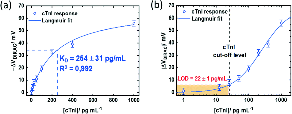 | ||
| Fig. 6 cTnI sensing performance of the GFET modified with PMAL for 2 h: Dirac point variations (ΔVDirac = VDirac ([cTnI]) − VDirac (buffer)) as a function of cTnI concentration using (a) a linear scale and (b) a logarithmic scale for better visualisation of the LoD and the cTnI cut-off level. | ||
Finally, the specificity of the signal induced by the cTnI binding to the aptamer immobilized at the graphene surface was assessed against two other cardiac biomarkers. GFETs functionalized with the same optimized PMAL incubation conditions (2 h) were exposed to increasing concentrations of either brain natriuretic peptide (BNP) or cardiac troponin T (cTnT). BNP is a hormone secreted in the heart ventricles, in response to ventricular stretching, used as a biomarker for heart failure diagnosis,53 while cTnT, similar to cTnI, is a subunit of the troponin complex also used as a biomarker for myocardial infarction.29 In the presence of BNP (Fig. 7a) or cTnT (Fig. 7b), only minor modifications of the transfer curve could be observed in the 1–1000 pg mL−1 concentration range. While cTnI specific binding induced a negative shift of the whole transfer curve, both non-specific target analytes induced a positive shift only to the n-branch of the curve. This modification induced by non-specific interactions resulted in a negative shift of the Dirac point, up to VDirac = +11 ± 2.5 mV for cTnT and VDirac = +2 ± 2.5 mV for the largest target concentration tested (1000 pg ml−1) (Fig. 7c and d). For comparison, the negative shift induced by the detection of the specific target at a 1000 pg ml−1 concentration was VDirac = −56 ± 2.5 mV, representing an absolute Dirac point shift variation 5 times larger than that for cTnT and 25 times larger than that for BNP.
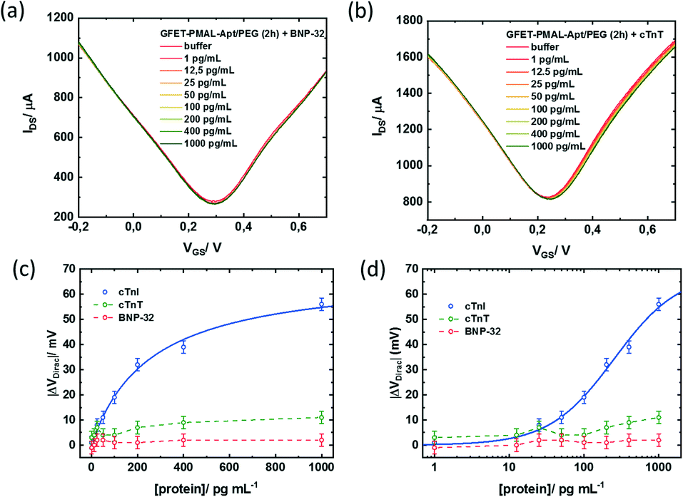 | ||
| Fig. 7 Non-specific response of the PMAL modified GFET: (a) transfer characteristics of GFET-aptamer/PEG (2 h PMAL incubation) after stabilization for increasing concentrations of (a) BNP-32 or (b) cTnT in 0.01× PBS/MgCl2 (1 mM) (pH 7.4) without washing steps, applied VDS = 50 mV. Absolute Dirac point variations (ΔVDirac = VDirac ([protein]) − VDirac (buffer)) as a function of cTnI (blue), cTnT (green) or BNP (red) concentration using (c) a linear scale and (d) a logarithmic scale. | ||
A variety of cTnI biosensors based on optical, electrochemical and electrical transduction have been reported,54 among which nanowire-based FET biosensors have shown LoD values typically ranging from 100 pg mL−1 down to 1 pg mL−1.55–58 Yet, the discussed GFET approach based on the use of optimized pyrene-based functionalization has a comparable high sensitivity to cTnI sensing, with the additional advantage of using considerably simpler fabrication processes, without the need of harsh and complex chemistry methods for the functionalization of the sensing area.
Conclusions
In this article, three different pyrene ligands were investigated not only for the interaction capability with CVD graphene, but also in terms of post-functionalization for biosensing. The results presented all point to a limited utility of PBASE due to the labile character of the hydroxysuccinimide ester. Using ferrocene as the model ligand, it could be shown that PBA is better suited but forms pyrene stacks rather than fully covered graphene interfaces. Non-specific interactions might easily take place on the nonmodified areas in this case. Pyrene carrying a maleimide tail clearly outperformed the other two pyrene surface anchors. Most interestingly, the time of immersion between graphene and PMAL has an important impact on the sensing performance of the GFET device. Using the sensing of cTnI as the model, it could be shown that 2 h incubation promotes the formation of a robust and functional biorecognition layer on the GFET for optimized sensor performance. With a limit of detection of 22 ± 1 pg mL−1 the performance of the GFET sensor is within the clinical important window of 40 pg mL−1, which is the cut-off for detection of myocardial ischemia. Troponin diagnostics thus evolved from a test to diagnose acute myocardial infarction (AMI) to one that allows early detection of cardiac injuries.Experimental
Materials
1-Pyrenebutyric acid (PBA), 1-pyrenebutyric acid N-hydroxysuccinimide ester (PBASE), aminoferrocene (Fc-NH2), 6-(ferrocenyl)hexanethiol (Fc-SH), 1-ethyl-3-(3-dimethylaminopropyl)carbodiimide hydrochloride (EDC), N-hydroxysuccinimide (NHS), phosphate buffered saline (PBS), magnesium sulfate (MgSO4), tetrabutylammonium hexafluorophosphate (NBu4FP6), ammonium persulfate ((NH4)2S2O8), polymethyl methacrylate (PMMA), tris(2-carboxyethyl)phosphine hydrochloride (TCEP) and thiolated-PEG4-methyl were purchased from Sigma-Aldrich and used as received. Pyrene maleimide (PMAL) was purchased from Lumiprobe GmbH, Germany. Interdigitated microelectrodes (ED-IDE1-Au w/o SU8) were purchased form Micrux Technologies, Spain. cTnI-specific DNA aptamer (5′-thiol TTT TTT CGT GCA GTA CGC CAA CCT TTC TCA TGC GCT GCC CCT CTT A-3′) was provided by Integrated DNA Technologies (Leuven, Belgium). Recombinant human cardiac troponin I protein (MW = 24 kDa) and recombinant human cardiac troponin T protein (MW = 36 kDa) were obtained from Abcam (Cambridge, UK). BNP-32 peptide (MW = 3.4 kDa) was obtained from BACHEM AG (Switzerland).Graphene synthesis
The monolayer graphene is grown by chemical vapor deposition (CVD) on commercial Cu foil from Alfa Aesar (high purity – 99.9999%). Graphene growth is carried out using a Jipelec JetFirst Rapid Thermal CVD (RTCVD). This system allows heating and cooling at high rates (10 °C s−1). The growth itself comprises heating, annealing, growth and cooling steps. We used a mixture of 100 sccm of argon and 5 sccm of dihydrogen during all the steps and 20 sccm of methane as a precursor during the growth phase. We first cut the Cu foil into small pieces (2.5 × 2.5 cm) and clean them with acetic acid, acetone and IPA for 5 min each under ultrasonication in order to remove all possible copper oxide and to produce the cleanest surface possible. We then put the pieces onto a Si wafer in the chamber. We proceed to evacuate the chamber to achieve a high vacuum (<5 × 10⁻⁵ bar) before starting, and then the sample is heated for 5 min from room temperature to 300 °C, followed by heating for 2 min from 300 °C to 1070 °C, annealing for 5 min, growth for 5 min and finally a quick cooling of the chamber using a water flow (with a decrease rate of 60 °C s 1 from 1000 to 700 °C), for 10 min to reach room temperature.FET sensor fabrication
Prior to graphene transfer, the interdigitated microelectrodes (ED-IDE1-Au w/o SU8, Micrux Technologies) are cleaned in an UV–ozone chamber (Jelight, USA) for 10 min followed by submersion for 15 min sequentially in 10 mL of acetone, iso-propanol and water. Finally, every chip is copiously rinsed with a large amount of water and dried under a nitrogen flow. The cleaned interfaces are placed in a plastic Petri dish and stored in a desiccator under vacuum. The cleaned IDEs are modified with trimethoxyphenylsilane (TMPS, 300 μL of TMPS in 15 mL of ethanol) in a plastic falcon tube for 1 h. Afterwards, the electrodes are immersed for 15 min in ethanol to remove excess silane compounds from the surface. Subsequently, the modified interfaces are blow dried with nitrogen and stored under vacuum. The chips are placed on a hot plate at 120 °C and ambient pressure for 2 h to anneal the formed monolayer and provide complete removal of the solvents from the surface. Graphene is directly transferred to these interfaces. For graphene transfer, a polymethyl methacrylate (PMMA) film of 200 nm in thickness is spin-coated onto the graphene/Cu foil and annealed at 110 °C with very slow heating and cooling rates (1 °C min−1) in order to prevent cracks in the graphene due to the difference of the thermal expansion coefficient between copper and graphene. The graphene on the back side of the Cu foil was removed by reactive ion etching (RIE) in an O2 plasma (50 W/100 mT/25 sccm/1 min). Copper foil etching was achieved in 0.2 M ammonium persulfate ((NH4)2S2O8) for 8 h, and the floating PMMA/graphene sample was put in DI water. This operation was repeated about 10 times in order to rinse the graphene from the etchant solution. Graphene transfer onto the IDE was achieved by submerging the IDE under the floating graphene/PMMA film. To remove traces of trapped water between graphene and the IDE and to increase the adhesion of graphene to the IDE, the substrate was placed on a hot plate and annealed at 90 °C for 30 min using slow heating and cooling rates (1 °C min−1). The PMMA layer was effectively removed by UV/ozone cleaning at 28–35 mW cm−2 for 5 min followed by a hot acetone rinse (50 °C for 180 min).Surface modification
Pyrene derivatives were dissolved in dry DMF at 5 mM and the interfaces immersed with constant agitation under ambient conditions for different time intervals. After the modification the interfaces were withdrawn, copiously washed with DMF and water and dried under a nitrogen flow. For PBA the carboxyl groups were activated via NHS/EDC by first adding 2 mM aqueous EDC solution onto the PBA modified interfaces for 30 min, followed by addition of 5 mM aqueous NHS solution for 30 min. The corresponding ferrocene derivatives (5 mM) in DMF (Fc-NH2 for PBA and PBASE; Fc-SH for PMAL) were drop-cast on the modified interfaces. The reaction time was 4 hours followed by washing in DMF and water.Electrical sensing
Electrical measurements were conducted using a source meter unit U2722A (Keysight Technologies, USA). All measurements were performed using a PMMA commercial flow cell (Micrux Technologies, Spain) with a fixed flow channel geometry (16 μL), ensuring a defined flow rate of 50 μL min−1 to minimize mass transport limitation of the analyte to the sensor surface in all experiments. A silver chloride wire (diameter 1 mm, Sigma-Aldrich) was used to operate the GFET device in a liquid gate configuration, with a constant source-drain bias (VDS) of 0.05 V, sweeping the gate voltage (VGS) between −0.2 V and 0.7 V.Biosensing
The cTnI-specific DNA aptamer was resuspended in 1× PBS buffer containing 1 mM of MgCl2. The aptamer solution (100 μg mL−1) was then heated at 90 °C for 5 min and cooled down slowly to room temperature to insure proper folding. A thiolated-PEG4-methyl was used to prevent non-specific adsorption on graphene. The PEG solution was prepared in the same buffer used for the aptamer with an aptamer/PEG molar ratio of 2:1. Both the aptamer and PEG solutions were diluted in a TCEP solution (1:1 volume ratio; 100 molar excess) for 20 min right before use in order to reduce eventual disulphide bonds. The GFET was then functionalized by adding both solutions to the graphene channel area, incubated for 2 h and rinsed with 0.01× PBS/MgCl2 (1 mM) buffer before electrical characterization. cTnI and BNP solutions were prepared in 0.01× PBS/MgCl2 (1 mM) buffer.
Characterization
Water contact angles were acquired with a contact angle meter (FTÅ 200, Data physics Inc, USA) at room temperature. A water droplet (about 8 μL) was dropped gently onto the interface, and the values reported are averages of five measurements made on different positions of the sample surface. The accuracy of the CA value was ±2°. The images were captured using a CCD digital camera. Raman spectroscopy measurements were performed on a LabRam HR Micro-Raman system (Horiba Jobin Yvon, France) combined with a 473 nm laser diode as the excitation source. Visible light was focused using a 100× objective. The scattered light was collected using the same objective in a backscattering configuration, dispersed using a 1800 mm focal length monochromator and detected using a CCD. A PalmSens4 Potentiostat/Galvanostat (PalmSens, The Netherlands) was used to perform cyclic voltammetry measurements. The potentiostat was connected to a three-electrode cell (Micrux, Spain) with an IDE acting as a working electrode, a Pt wire as the counter electrode and Ag/AgCl as the reference electrode. The cyclic voltammograms were recorded with a scan rate of 100 mV s−1 and a potential step of 0.01 V.Author contributions
VM: graphene transfer and electrochemical measurements; AH: field effect measurements and sensing; TR: cTnI sensing and device design; PA: funding; HH: graphene growth; VB: surface characterization by TEM; RB: writing and proofreading, WK: funding and proofreading; SS: conception, funding and overall supervision.Conflicts of interest
There are no conflicts to declare.Acknowledgements
Financial support from the Centre National de la Recherche Scientifique (CNRS), the University of Lille and the Agence Nationale pour la Recherche (ANR-2020-PADISC) is acknowledged.References
- S. Wang, M. Z. Hossain, K. Shinozuka, N. Shimizu, S. Kitada, T. Suzuki, R. Ichige, A. Kuwana and H. Kobayashi, Biosens. Bioelectron., 2020, 165, 112363 CrossRef CAS PubMed.
- G. Ambrosio, A. Brown, L. Daukiya, G. Drera, G. Di Santo, L. Petaccia, S. De Feyter, L. Sangaletti and S. Pagliara, Nanoscale, 2020, 12, 9032–9037 RSC.
- I. Prattis, E. Hui, P. Gubeljak, G. S. K. Schierle, A. Lombardo and L. G. Occhipinti, Trends Biotechnol., 2021, 39, 1065–1077 CrossRef CAS PubMed.
- G. Seo, G. Lee, M. J. Kim, S.-H. Baek, M. Choi, K. B. Ku, C.-S. Lee, S. Jun, D. Park and H. G. Kim, ACS Nano, 2020, 14, 5135–5142 CrossRef CAS PubMed.
- Z. Hao, Y. Luo, C. Huang, Z. Wang, G. Song, Y. Pan, X. Zhao and S. Liu, Small, 2021, 2101508 CrossRef CAS PubMed.
- R. Sharma, J. H. BAik, C. J. Perera and M. S. Strano, Nano Lett., 2010, 10, 398–405 CrossRef CAS PubMed.
- G. L. C. Paulus, Q. H. Wang and M. S. Strano, Acc. Chem. Res., 2012, 46, 160–170 CrossRef PubMed.
- Q. H. Wang, Z. Jin, K. K. Kim, A. J. Hilmer, G. L. C. Paulus, C.-H. Shih, M.-H. Ham, J. D. Sanchez-Yamagishi, K. Watanabe, T. Taniguchi, J. Kong, P. Jarillo-Herrero and M. S. Strano, Nat. Chem., 2012, 4, 724 CrossRef CAS PubMed.
- B. A. Lehner, D. Benz, S. A. Moshkalev, A. S. Meyer, M. A. Cotta and R. Janissen, ACS Appl. Nano Mater., 2021, 8334 CrossRef CAS PubMed.
- T. Saito, M. Tabata, A. Isobayashi, H. Miki, Y. Miyahara and Y. Sugizaki, Langmuir, 2021, 37, 4997–5004 CrossRef CAS PubMed.
- A. Lopez and J. Liu, Adv. Intell. Syst., 2020, 2, 2000123 CrossRef.
- C. K. Chua and M. Pumera, Chem. Soc. Rev., 2013, 43, 3222–3233 RSC.
- J. Lu, A. Lipatov, N. S. Vorebeva, D. S. Muratov and A. Sinitskii, Adv. Electron. Mater., 2018, 4, 1800021 CrossRef.
- V. Georgakilas, J. N. Toiwari, C. Kemp, J. A. Perman, A. B. Boulinos, K. S. Kim and R. Zboril, Chem. Rev., 2016, 9, 5464–5519 CrossRef PubMed.
- P. Aspermair, V. Mishyn, J. Bintinger, H. Happy, K. Bagga, P. Subramanian, W. Knoll, R. Boukherroub and S. Szunerits, Anal. Bioanal. Chem., 2021, 413, 779–787 CrossRef CAS PubMed.
- M. Singh, M. Holzinger, M. Tabrizian, S. Winters, N. C. Berner, S. Cosnier and G. S. Duesberg, J. Am. Chem. Soc., 2015, 137, 2800–2803 CrossRef CAS PubMed.
- M. Hinnemo, J. Zhao, P. Ahlberg, C. Hagglund, V. Djurberg, R. H. Scheicher, S.-S. Zhang and Z. Zhang, Langmuir, 2014, 33, 3588–3593 CrossRef.
- M. Cao, A. Fu, Z. Wang, J. Liu, N. Kong, X. Zong, H. Liu and J. J. Gooding, J. Phys. Chem. B, 2014, 118, 2650–2659 CAS.
- K. Thodkar, P.-A. Cazade, F. Bergmann, E. Lopez-CAlle, D. Thompsron and D. Heindl, ACS Appl. Mater. Interfaces, 2021, 13, 9134–9142 CrossRef CAS PubMed.
- C. Ingrosso, G. V. Bianco, R. Corricelli, R. Comparelli, D. Altamura, A. Agostiano, M. Striccoli, M. Losurdo, M. L. Curri and G. Bruno, ACS Appl. Mater. Interfaces, 2015, 7, 4151–4159 CrossRef CAS PubMed.
- F. Halouane, R. Jijie, D. Meziane, C. Li, S. K. Singh, J. Bouckaert, J. Jurazek, S. Kurungot, A. Barras and M. Li, J. Mater. Chem. B, 2017, 5, 8133–8142 RSC.
- F. Chekin, V. Vasilescu, R. Jijie, S. K. Singh, S. Kurungot, M. Iancu, G. Badea, R. Boukherroub and S. Szunerits, Sens. Actuators, B, 2018, 261, 180–187 CrossRef.
- Y. Huang, X. Dong, Y. Shi, C. M. Li, L.-J. Li and P. Chen, Nanoscale, 2010, 2, 1485–1488 RSC.
- D. K. H. Tsang, C. W. Tyler, J. Lieberthal, I. E. Dunlop, S. Ramadan, A. E. del Rio Hernandez and N. Klein, Sci. Rep., 2019, 9, 13946 CrossRef PubMed.
- N. Nekrasov, D. Kireev, A. Emelianov and I. Bobrinetskiy, Toxins, 2019, 11, 550 CrossRef CAS PubMed.
- S. Bailey, D. Visontai, C. J. Lambert, M. R. Bryce, H. Frampton and D. Chappell, J. Chem. Phys., 2014, 140, 054708 CrossRef PubMed.
- G. Xu, J. Abbott, L. Qin, K. Y. Yeung, Y. Song, H. Yoon, J. Kong and D. Ham, Nat. Commun., 2014, 5, 4866 CrossRef CAS PubMed.
- X. Chen, Y. Liu, X. Fang, Z. Li, H. Pu, J. Chang, J. Chen and S. Mao, Biosens. Bioelectron., 2019, 126, 664–671 CrossRef CAS PubMed.
- G. E. Fenoy, W. A. Marmisollé, O. Azzaroni and W. Knoll, Biosens. Bioelectron., 2020, 148, 111796 CrossRef CAS PubMed.
- C. Reiner-Rozman, M. Larisika, C. Nowak and W. Knoll, Biosens. Bioelectron., 2015, 70, 21–27 CrossRef CAS PubMed.
- G. Seo, G. Lee, M. J. Kim, S. H. Baek, M. Choi, K. B. Ku, C. S. Lee, S. Jun, D. Park, H. G. Kim, S. J. Kim, J. O. Lee, B. T. Kim, E. C. Park and S. I. Kim, ACS Nano, 2020, 14, 5135–5142 CrossRef CAS PubMed.
- Y. Huang, X. Dong, Y. Liu, L.-J. Li and P. Chen, J. Mater. Chem., 2011, 21, 12358–12362 RSC.
- S. Mao, J. Chang, H. Pu, G. Lu, Q. He, H. Zhang and J. Chen, Chem. Soc. Rev., 2017, 46, 6872–6904 RSC.
- S. O. Woo, J. Froberg, Y. Pan, S. Tani, B. R. Goldsmith, Z. Yang and Y. Choi, ACS Appl. Electron. Mater., 2020, 2, 913–919 CrossRef CAS PubMed.
- H. Chen, P. Chen, J. Huang, R. Selegård, M. Platt, A. Palaniappan, D. Aili, A. I. Y. Tok and B. Liedberg, Anal. Chem., 2016, 88, 2994–2998 CrossRef CAS PubMed.
- V. Mishyn, T. Rodrigues, Y. R. Leroux, P. Aspermair, H. Happy, J. Bintinger, C. Kleber, R. Boukherroub, W. Knoll and S. Szunerits, Nanoscale Horiz., 2021, 6, 819–829 RSC.
- Y. Hao, Y. Wang, L. Wang, Z. Ni, Z. Wang, R. Wang, C. K. Koo, Z. Shen and J. T. Thong, Small, 2010, 6, 195–200 CrossRef CAS PubMed.
- S. Szunerits, V. Mishyn, I. Grabowska and R. Boukherroub, Biosens. Bioelectron., 2019, 131, 287–298 CrossRef CAS PubMed.
- S. Upasham, A. Tanak and S. Prasad, Adv. Health Care Technol., 2018, 4, 1–13 CrossRef.
- G. Romiti, R. Cangemi, F. Toriello, E. Ruscio, S. Sciomer, F. Moscucci, M. Vincenti, C. Crescioli, M. Proietti, S. Basili and V. Raparelli, Cardiovasc. Ther., 2019, 9546931 CAS.
- L. Gammelgaard, J. M. Caridad, A. Cagliani, D. M. Mackenzie, D. H. Petersen, T. J. Booth and P. Bøggild, 2D Mater., 2014, 1, 035005 CrossRef CAS.
- S. Xu, J. Zhan, B. Man, S. Jiang, W. Yue, S. Gao, C. Guo, H. Liu, Z. Li and J. Wang, Nat. Commun., 2017, 8, 1–10 CrossRef PubMed.
- T. Kuamit, M. Ratanasak, C. Rungnim and V. Parasuk, J. Mol. Model., 2017, 23, 1–9 CrossRef CAS PubMed.
- X. Dong, D. Fu, W. Fang, Y. Shi, P. Chen and L. J. Li, Small, 2009, 5, 1422–1426 CrossRef CAS.
- Y. Liu, L. Yuan, M. Yang, Y. Zheng, L. Li, L. Gao, N. Nerngchamnong, C. T. Nai, C. S. Sangeeth and Y. P. Feng, Nat. Commun., 2014, 5, 1–8 Search PubMed.
- L. H. Hess, M. Seifert and J. A. Garrido, Proc. IEEE, 2013, 101, 1780–1792 CAS.
- S. Xu, J. Zhan, B. Man, S. Jiang, W. Yue, S. Gao, C. Guo, H. Liu, Z. Li, J. Wang and Y. Zhou, Nat. Commun., 2017, 8, 14902 CrossRef CAS PubMed.
- N. I. Khan and E. Song, Sensors, 2021, 21, 1335 CrossRef CAS PubMed.
- G. Wu, Z. Dai, X. Tang, Z. Lin, P. K. Lo, M. Meyyappan and K. W. C. Lai, Adv. Healthcare Mater., 2017, 6, 1700736 CrossRef PubMed.
- X. Wang, Z. Hao, T. R. Olsen, W. Zhang and Q. Lin, Nanoscale, 2019, 11, 12573–12581 RSC.
- X. Dong, Y. Shi, W. Huang, P. Chen and L. J. Li, Adv. Mater., 2010, 22, 1649–1653 CrossRef CAS PubMed.
- C. T. Lin, P. T. K. Loan, T. Y. Chen, K. K. Liu, C. H. Chen, K. H. Wei and L. J. Li, Adv. Funct. Mater., 2013, 23, 2301–2307 CrossRef CAS.
- H. Yasue, M. Yoshimura, H. Sumida, K. Kikuta, K. Kugiyama, M. Jougasaki, H. Ogawa, K. Okumura, M. Mukoyama and K. Nakao, Circulation, 1994, 90, 195–203 CrossRef CAS.
- T. Rodrigues, V. Mishyn, A. Bozdogan, Y. Leroux, H. Happy, A. Kasry, R. Boukherroub, J. Dostalek, P. Aspermair and J. Bintinger, Annals of Clinical and Medical Case Reports, 2021, 6, 1–16 CrossRef.
- T. Kong, R. Su, B. Zhang, Q. Zhang and G. Cheng, Biosens. Bioelectron., 2012, 34, 267–272 CrossRef CAS PubMed.
- J. Luo, S. Li, M. Xu, M. Guan, M. Yang, J. Ren, Y. Zhang and Y. Zeng, AIP Adv., 2020, 10, 115205 CrossRef CAS.
- S.-M. Chang, S. Palanisamy, T.-H. Wu, C.-Y. Chen, K.-H. Cheng, C.-Y. Lee, S.-S. F. Yuan and Y.-M. Wang, Sci. Rep., 2020, 10, 1–11 CrossRef PubMed.
- M. D. Prakash, B. V. Krsihna, B. Satyanarayana, N. A. Vignesh, A. K. Panigrahy and S. Ahmadsaidulu, Silicon, 2021, 1–8 Search PubMed.
- N. Nakatsuka, K.-A. Yang, J. M. Abendroth, K. M. Cheung, X. Xu, H. Yan, C. Zhao, B. Zhu, Y. S. Rim, Y. Yang, P. S. Weiss, M. N. Stonjanovic and A. M. Andrews, Science, 2018, 362, 319–324 CrossRef CAS PubMed.
Footnote |
| † Equal contribution. |
| This journal is © The Royal Society of Chemistry 2022 |