
 Open Access Article
 This Open Access Article is licensed under a Creative Commons Attribution-Non Commercial 3.0 Unported Licence
Substituent engineering of the diboron molecular architecture for a nondoped and ultrathin emitting layer†
Tien-Lin
Wu
 *a,
Jian
Lei
ab,
Chia-Min
Hsieh
a,
Yi-Kuan
Chen
a,
Pei-Yun
Huang
a,
Po-Ting
Lai
c,
Tsu-Yu
Chou
c,
Wei-Chen
Lin
d,
Wei
Chen
d,
Chi-Hua
Yu
d,
Liang-Yan
Hsu
b,
Hao-Wu
Lin
c and
Chien-Hong
Cheng
*ae
*a,
Jian
Lei
ab,
Chia-Min
Hsieh
a,
Yi-Kuan
Chen
a,
Pei-Yun
Huang
a,
Po-Ting
Lai
c,
Tsu-Yu
Chou
c,
Wei-Chen
Lin
d,
Wei
Chen
d,
Chi-Hua
Yu
d,
Liang-Yan
Hsu
b,
Hao-Wu
Lin
c and
Chien-Hong
Cheng
*ae
aDepartment of Chemistry, National Tsing Hua University, Hsinchu, 300044, Taiwan. E-mail: tlwu@mx.nthu.edu.tw; chcheng@mx.nthu.edu.tw
bInstitute of Atomic and Molecular Sciences, Academia Sinica, Taipei, 10617, Taiwan
cDepartment of Materials Science and Engineering, National Tsing Hua University, Hsinchu, 300044, Taiwan
dDepartment of Engineering Science, National Cheng Kung University, Tainan, 701, Taiwan
eDepartment of Chemistry, National Sun Yat-sen University, Kaohsiung, 80424, Taiwan
First published on 18th October 2022
Abstract
Owing to the high technology maturity of thermally activated delayed fluorescence (TADF) emitter design with a specific molecular shape, extremely high-performance organic light-emitting diodes (OLEDs) have recently been achieved via various doping techniques. Recently, undoped OLEDs have drawn immense attention because of their manufacturing cost reduction and procedure simplification. However, capable materials as host emitters are rare and precious because general fluorophores in high-concentration states suffer from serious aggregation-caused quenching (ACQ) and undergo exciton quenching. In this work, a series of diboron materials, CzDBA, iCzDBA, and tBuCzDBA, is introduced to realize the effect of steric hindrance and the molecular aspect ratio via experimental and theoretical studies. We computed transition electric dipole moment (TEDM) and molecular dynamics (MD) simulations as a proof-of-concept model to investigate the molecular stacking in neat films. It is worth noting that the pure tBuCzDBA film with a high horizontal ratio of 92% is employed to achieve a nondoped OLED with an excellent external quantum efficiency of 26.9%. In addition, we demonstrated the first ultrathin emitting layer (1 nm) TADF device, which exhibited outstanding power efficiency. This molecular design and high-performance devices show the potential of power-saving and economical fabrication for advanced OLEDs.
Introduction
Organic light-emitting diodes (OLEDs) have achieved very high efficiency by employing thermally activated delayed fluorescence (TADF)1 and molecular self-alignment2 so far. Pure-organic emitters with TADF properties possess reverse intersystem crossing (RISC)3 to achieve electroluminescent (EL) devices with nearly 100% internal quantum efficiency (IQE).4,5 Moreover, the enhancement of the device out-coupling efficiency was realized by employing dopant emitters with highly horizontal emitting dipole orientation.2,6 Generally, the molecular shape and transition dipole moment can cause a certain molecular orientation and alignment in thin film, and the rod-like, disk-like molecules2,7,8 show a trend of preferential horizontal ratio (up to ∼97%). With the cooling substrate method,9 the completely horizontal orientation (100%) could be even achieved. Recently, the doping technique has played a vital role in high-performance OLEDs and commercial panels because most luminophores suffer from serious emission quenching in high-concentration doped and neat films. To avoid a harmful nonradiative process occurring, the guest/host system in the emitting layer (EML) has dominated most OLED configurations nowadays. However, the co-doping method in the fabrication process requires accurate deposition rate control and excessive use of chemicals, which might generate extra chemical waste and make recycling difficult. Furthermore, doped-type TADF OLEDs often show a high efficiency roll-off at a high luminance because exciton annihilation arises when TADF emitters with a long excited-state lifetime cause singlet–triplet and triplet–triplet annihilation (STA and TTA),10 which means a high concentration of excitons is formed in the EML and will increase the probability of annihilation and energy loss.11Previous studies pointed out that an increasing doping ratio (especially for nondoped) of the EML can reduce the efficiency roll-off issue.12,13 However, emitters with an aggregation-quenching nature in high-concentration doping status still cause a considerable issue. To deal with the dilemma of the high-performance and nondoped OLEDs, the design and investigation of the host emitter is the primary task. Fluorescence aggregation-caused quenching (ACQ) generally occurs due to the high tendency towards π–π stacking of fluorophores. Specifically for emitters in the solid state, the ACQ effct is obviously harmful to optical applications, resulting in low emission intensity and considerable efficiency loss. The strategy of twisted structure or bulky substituent is a technique for reducing the degree of intermolecular aggregation in thin films. An emitter with a sterically hindered group14 or conformational heterogeneity15 might increase the distance between nearby molecules in the packing status. However, there is no systematic guide for designing efficient nondoped emitters with precise substituent positions. In another aspect, the development of nondoped OLEDs offers an avenue for the exploration of an extremely simplified device, which makes the EML ultrathin and greatly reduces its power consumption.16 The OLEDs with around 1 nm of EML thickness, low driving voltage (<3.0 V), and high efficiency have been demonstrated by Ma et al., who reported various color OLEDs and WOLEDs by using phosphorescent dyes.17–19 With the nondoped and ultrathin EML, the OLEDs can have the merits of energy-saving and cost-effective fabrication simultaneously.
In our previous study, two diboron-based TADF materials, CzDBA and tBuCzDBA, can be applied to high-performance OLEDs due to their high PLQYs, short delayed lifetimes, and rod-like molecular shape.20 In particular, we noticed that these emitters have less self-quenching ability in neat films, which could also account for a low efficiency roll-off device. Notably, for tBuCzDBA with the tert-butyl group at the 3,6-position of the carbazole donor, a slight reduction of PLQY (86 to 84%) and a reduced red-shifted PL band (8 nm) in the neat film were observed compared to its doped film condition (10 wt% in CBP). Therefore, diboron compounds with a twisted molecular structure and bulky substituents are capable of lowering the degree of aggregation. As per our expectation, CzDBA has been employed for a single-layer emitter device by Kotadiya et al.,21 and their nondoped device shows good efficiency of 19% external quantum efficiency (EQE) and a relatively long operation lifetime up to 1880 hours. Furthermore, the out-coupling efficiency is estimated to be 26% by varying the CzDBA thickness.22
Herein, we propose a design rule to demonstrate the importance of bulky substituent positions toward molecular design in the pristine solid state. The proposed strategy of engineering the diboron molecular shape with a highly horizontal emitting dipole orientation is shown in Scheme 1. We assume that the higher molecular aspect and suitable bulky group position can promote the horizontal ratio in a neat film. To prove the concept, two modified CzDBA derivatives with bulky substituents on the middle or terminal side are introduced to investigate the packing distance, emission quenching properties, and horizontal ratio. Our theoretical calculations and molecular dynamics simulations all support our hypothesis. As a result, tBuCzDBA with the bulky substituent and highest aspect ratio23 not only decreases the ACQ effect but also exhibits the highest horizontal ratio (92%) under neat film conditions. In contrast, iCzDBA displays the lowest horizontal ratio (77%), which is even lower than that of basic CzDBA (88%). Remarkably, the nondoped device with tBuCzDBA without any doping technique exhibits an excellent EQE of 26.9% among pure-organic nondoped OLEDs.24–27 To further reduce the EML thickness, the ultrathin TADF OLED is demonstrated by employing only 1 nm of tBuCzDBA. It is worth noting that ultrathin EML devices show a high power efficiency of 95.3 lm W−1 and the lowest driving voltage of 2.1 V, which are rather comparable to recent state-of-the-art nondoped OLEDs.
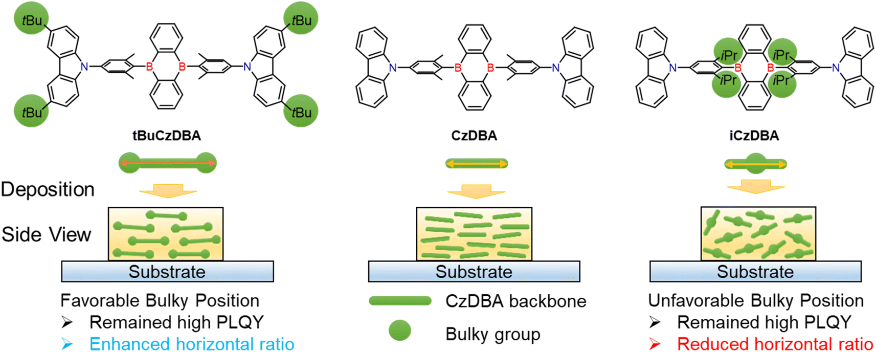 | ||
| Scheme 1 The molecular structures of the diboron-based materials and the substituent engineering strategy of the emitters in neat films. | ||
Results and discussion
Synthesis and characterization
We had reported and synthesized a series of 9,10-dihydro-9,10-diboraanthracene (DBA) compounds20via the nucleophilic arylation of lithiated carbazole derivatives with 9,10-dibromo-9,10-diboraanthracene (DBDBA).28 In comparison with tBuCzDBA, the bulky isopropyl group was introduced into the middle phenyl group of CzDBA for the synthesis of iCzDBA. Three DBA-based structures are shown in Scheme 1 and the synthetic details of iCzDBA are shown in the ESI (Scheme S1 and Fig. S1–S4†). Thermal gravimetric analysis (TGA) and differential scanning calorimetry (DSC) measurements under a nitrogen atmosphere were performed. iCzDBA has lower thermal stability compared to CzDBA and tBuCzDBA. The decomposition temperature (Td) is around 338 °C and the glass transition temperature (Tg) was not detected (Fig. S5†). The HOMO and LUMO levels of iCzDBA are −5.91 and −3.31 eV, respectively, determined from photoelectron spectroscopy (Fig. S6†) and optical band gap (Eg). The HOMO and LUMO distributions in iCzDBA were well separated between Cz and DBA motifs by using density functional theory (DFT) calculation at the BMK/6-31G* level, as shown in Fig. S7.† The details of material characterization are shown in the Experimental section.All single crystals of DBA derivatives were grown and prepared by the sublimation method under low pressure (10−6 torr). The cell parameters are summarized in Table S1,† while crystal packing and stacking distance are shown in Fig. S8.† Although the single-crystal structures of CzDBA and tBuCzDBA have been revealed in a previous study,20 the crystal stacking details and comparison are further discussed here. iCzDBA has a D-A-D framework and rod-like design, and all organoboron derivatives adopt a highly twisted structure with two dihedral angles between the disubstituted phenylene bridge and the neighboring Cz/DBA group, as shown in Fig. S9.† Except for iCzDBA, the larger dihedral angles that appear between the bridge group and the DBA acceptor are around 78°. The isopropyl groups of iCzDBA make the single-crystal structure slightly torsional and asymmetric. Additionally, CzDBA, iCzDBA, and tBuCzDBA packed in the C2/c, P21/c, and P![[1 with combining macron]](https://www.rsc.org/images/entities/char_0031_0304.gif) packing motif, respectively. The crystal packing of the three compounds was step-like stacking. tBuCzDBA with the largest bulky group exhibits a different crystalline system (triclinic) from others (monoclinic), showing a herringbone-type arrangement along the a axis in the crystal cell. The closest intermolecular distance of the DBA plane between two adjacent molecules is 6.12, 7.28 and 7.46 Å, respectively, for CzDBA, iCzDBA, and tBuCzDBA. The results showed that the values are higher than 6.0 Å, which might indicate that there is barely π–π interaction between nearby molecules in crystal packing. Therefore, iCzDBA and tBuCzDBA with additional bulky groups truly enlarge the distance and become more loose packing, which reveals that the further reduction of the ACQ process might exist in their neat films.29 To realize whether the dimers exist or not in pristine solid films, we performed TDDFT simulations of the three emitters. Their singlet excitations are mainly intramolecular CT transitions, as evidenced by the FMOs (Fig. S7†) and “holes” and “electrons” equally distributed on two molecules (Fig. 1), implying that dimer formation does not occur to a significant extent in these three molecules. Therefore, undesirable interactions may be suppressed due to crystal packing and stacking distance in their neat films.
packing motif, respectively. The crystal packing of the three compounds was step-like stacking. tBuCzDBA with the largest bulky group exhibits a different crystalline system (triclinic) from others (monoclinic), showing a herringbone-type arrangement along the a axis in the crystal cell. The closest intermolecular distance of the DBA plane between two adjacent molecules is 6.12, 7.28 and 7.46 Å, respectively, for CzDBA, iCzDBA, and tBuCzDBA. The results showed that the values are higher than 6.0 Å, which might indicate that there is barely π–π interaction between nearby molecules in crystal packing. Therefore, iCzDBA and tBuCzDBA with additional bulky groups truly enlarge the distance and become more loose packing, which reveals that the further reduction of the ACQ process might exist in their neat films.29 To realize whether the dimers exist or not in pristine solid films, we performed TDDFT simulations of the three emitters. Their singlet excitations are mainly intramolecular CT transitions, as evidenced by the FMOs (Fig. S7†) and “holes” and “electrons” equally distributed on two molecules (Fig. 1), implying that dimer formation does not occur to a significant extent in these three molecules. Therefore, undesirable interactions may be suppressed due to crystal packing and stacking distance in their neat films.
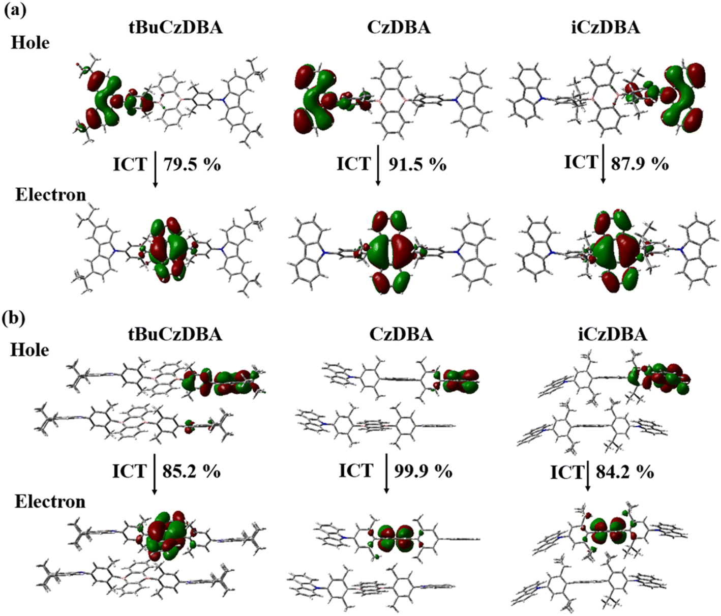 | ||
| Fig. 1 The natural transition orbitals (NTO) of CzDBA, iCzDBA, and tBuCzDBA of (a) single-crystal structures and (b) dimer crystal structures are calculated at the BMK/6-31G* level. | ||
Theoretical prediction of molecular orientation
In order to investigate the molecular orientation in neat films, we looked into the optimized structure for each molecule and computed the TEDM with the optimized S1 state of crystal structures (Fig. 2a). In the crystal-packing diagram, the three molecules tend to be aligned nearly parallel to their acceptor planes; thus, the TEDMs of CzDBA, iCzDBA, and tBuCzDBA were simulated with their corresponding acceptor moieties as the x–y plane. Eventually, in DBA derivatives, the direction of TEDM is more elongated along the long molecular axis, which could be attributed to the larger contribution of the acceptor unit with an expanded plane to the terminal carbazole part. All TEDM vectors of the three molecules mainly aligned on the plane of their corresponding acceptor moieties, and the TEDM vectors of the CzDBA and tBuCzDBA had lower z components, which reveals the high horizontal emitting dipole orientation features.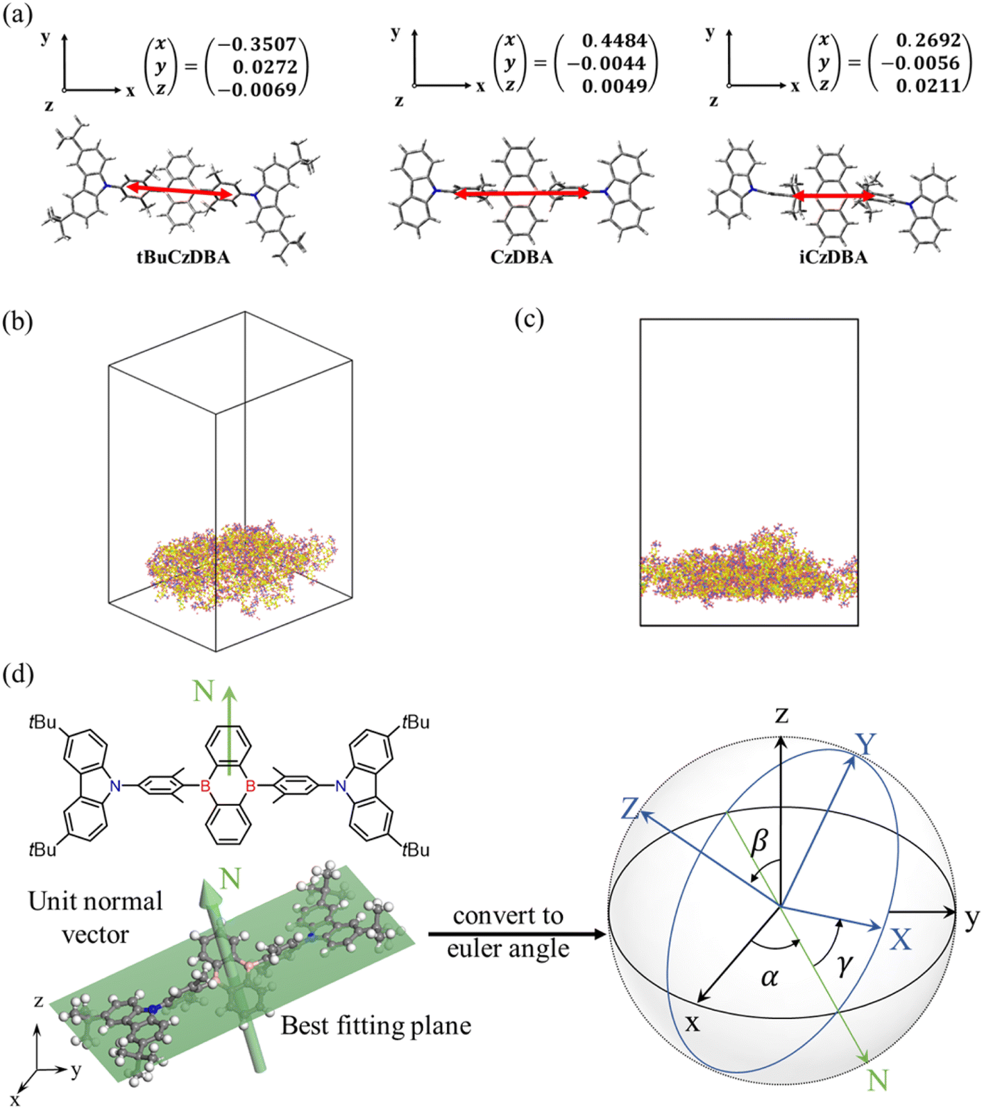 | ||
| Fig. 2 (a) The transition dipole moment vectors and the direction of calculated transition dipole moments for CzDBA, iCzDBA, and tBuCzDBA relative to the coordinate of the molecular structure. (b) Molecular representation of the deposition layer. (c) Deposition layer structure after cooling and equilibrium. (d) The representation of the molecular plane and the direction of unit normal; the stereographic projections are applied to examine the preferred orientation of each amorphous layer. | ||
As shown in Fig. 2b–c and Fig. S10,† a significant difference was found among CzDBA, iCzDBA, and tBuCzDBA using nonequilibrium molecular dynamics (NEMD). The methods and parameters for simulations are summarized in Table S3† and the Experimental section. Moreover, we used stereographic projections to represent the orientation distribution of each molecule, as shown in Fig. 2d. The x, y, and z axes are shown as (001), (010), and (001), respectively. Fig. S11† reveals a horizontal alignment for each system. As a result, the orientation of the tBuCzDBA amorphous layer indicates the normal discretion of each molecule toward the (001) direction. On the contrary, CzDBA and iCzDBA show less significant difference or preferred orientations. Accordingly, tBuCzDBA possesses a preferentially horizontal orientation in both TEDM calculation and MD simulation, which could establish a basis for constructing nondoped OLEDs with high light out-coupling efficiency.
Photophysical properties
The comparison of CzDBA and tBuCzDBA between the doped film and neat film has been previously reported,20 and reduced self-quenching characteristics have been observed. The photophysical properties of newly synthesized iCzDBA are similar to those of CzDBA in solution and the doped CBP film, as shown in Fig. S12.† iCzDBA shows a maximum absorption peak at 344 nm, assigned to a π to π* transition. The intramolecular charge transfer (ICT) absorption is likely assigned as the broad shoulder band that appears around 420 nm. Fig. S12† shows the obvious solvent effect in the PL spectra of iCzDBA, and the emission maximum observed at 526 nm in toluene shifted to 586 nm in dichloromethane, which further supports the ICT characteristics. The similar ΔEST value of 33 meV, which is very close to that of CzDBA, was determined via the fluorescence and phosphorescence spectra of the 10 wt% iCzDBA doped CBP film. Nevertheless, the photophysical properties of iCzDBA in the neat film are different from those of CzDBA. Fig. 3 exhibited the emission peaks for CzDBA, iCzDBA, and tBuCzDBA in neat film, which are 540, 538, and 561 nm, respectively. And, they have the peaks red-shifted by 16, 10, and 8 nm, compared with their corresponding 10 wt% doped CBP films. The photophysical data of doped and neat films are recorded in Table S4.† The emission decay curves of the doped film and neat film are shown in Fig. 4a–c. For the pristine films, the lifetimes of delayed components (τd) were reduced to 1.0, 1.4, and 1.2 μs for CzDBA, iCzDBA, and tBuCzDBA, respectively, compared with each doping condition (10 wt% in CBP). Significantly, their PLQYs in neat films still remain at high values of 90.6%, 88.0%, and 84.0% for CzDBA, iCzDBA, and tBuCzDBA, respectively. The rate constants of RISC (kRISC) in neat films were calculated to be 2.36 × 10⁶ s−1, 1.92 × 10⁶ s−1, and 2.02 × 10⁶ s−1, respectively, for CzDBA, iCzDBA, and tBuCzDBA. The employed method30 and all parameters are summarized in Table S5.† By comparing the results between the neat film and doped film, we believe the shorter τd in neat films accounts for the factor, generating relatively higher kRISC, and the trend was consistent with the reported results from the nondoped emitter film.11,12,31 However, the relatively serious ACQ effect still existed in CzDBA, due to the highest 16 nm emission red-shift and a 9.4% decline of PLQYs between the doped and neat films. In a similar manner, the time-resolved PL of CzDBA also exhibited a relatively dramatic difference between doped and neat films, compared to the spectra from iCzDBA and tBuCzDBA. In addition, the emission quenching level between doped and neat films probably correlates with the trends of the closest distance in single-crystal packing. Notably, tBuCzDBA displays the longest distance of 7.46 Å; thus, the most reduced self-quenching phenomenon was measured among the three DBA compounds. In short, the steric hindrance of the tert-butyl or isopropyl group has been evidenced to disperse the molecular aggregation29 and further reduce the ACQ process in neat films.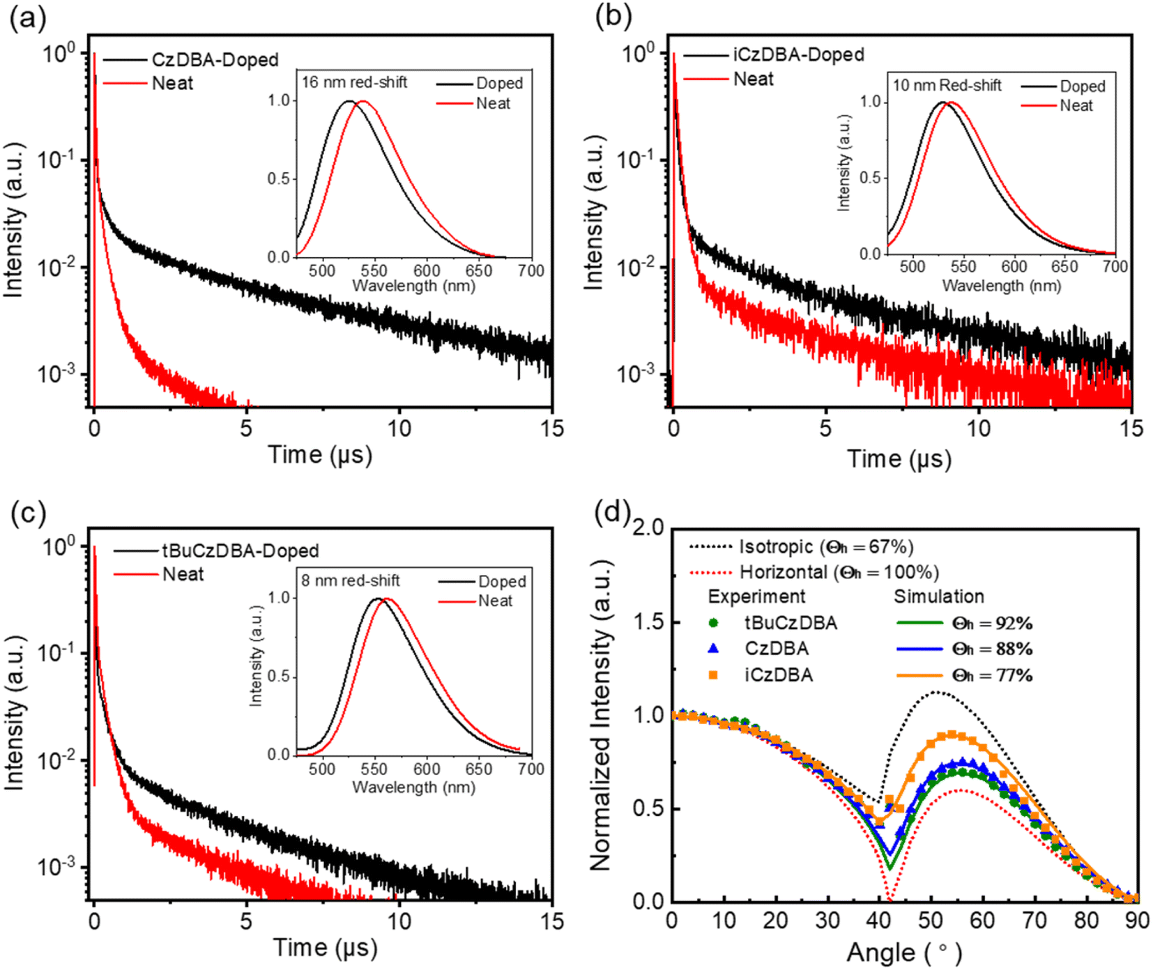 | ||
| Fig. 3 (a) Transient PL decay curves and fluorescence spectra in the inset of doped and neat films for (a) CzDBA, (b) iCzDBA, and (c) tBuCzDBA. (d) Variable-angle PL measurements of all 30 nm-thick neat films. | ||
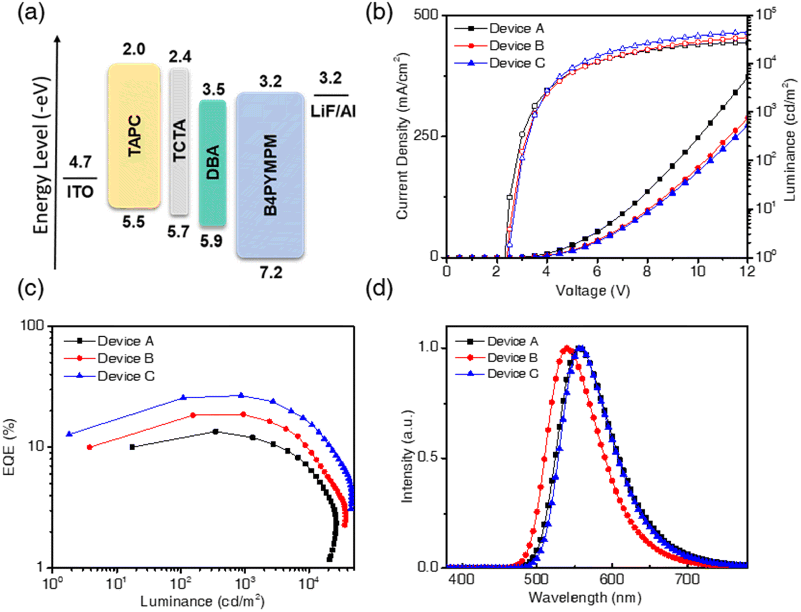 | ||
| Fig. 4 (a) Nondoped device configurations and energy levels. (b) Current density and luminance versus voltage characteristics. (c) External quantum efficiency versus luminance characteristics. (d) Electroluminescence spectra at 8 V. | ||
According to the reported literature,7 the molecular design containing rod-like and linear-type structures is suggested for increasing the horizontal emitting dipole orientation (Θh) in thin films. Specifically for the high aspect ratio design,32,33 a molecule with the long axis tends to parallelly lie to the substrate plane under vacuum evaporated deposition. The horizontal ratios of DBA derivatives in CBP were measured and analyzed by using variable-angle PL measurement, showing a relatively high Θh around 83–84%.20 Fig. S13† shows that the Θh of iCzDBA was determined to be 84% in the 10 wt% doped CBP film, due to the similar structure of CzDBA. To our surprise, the experimental results determined from their neat films are significantly different from those of their doped films. The Θh of CzDBA, iCzDBA, and tBuCzDBA in their neat films was determined to be 88%, 77%, and 92%, respectively, as shown in Fig. 3d. The trend of Θh is consistent with the spectroscopic ellipsometry characterization of 100 nm-thick neat films (Fig. S14†). Fluorescence and phosphorescence dyes with a horizontal ratio higher than 90%32–35 are rare. More importantly, the difference of emitting dipole orientation between neat and doped films was observed, indicating the significance of molecular shape for enhanced horizontal ratio in neat films. In order to engineer the molecular structure for low emission quenching and high Θh, tBuCzDBA with the highest aspect ratio manifest both advantages. Compared to iCzDBA, tBuCzDBA with bulky groups added on the terminal side of CzDBA truly extends the long axis, modifying the anisotropic orientation and further increasing the Θh to 92% in the neat film. The results are in good agreement with the TEDM calculations and MD simulations.
Nondoped and ultrathin EML devices
To study the performance of nondoped OLEDs, we fabricated the EL devices A, B, and C by using CzDBA, iCzDBA, and tBuCzDBA, respectively, as the host emitters. These nondoped devices without any doping technique were fabricated via the four-organic-layer configuration: ITO/TAPC (50 nm)/TCTA (10 nm)/diboron compounds (15 nm)/B4PYMPM (65 nm)/LiF (1 nm)/Al (100 nm), where di-[4-(N,N-di-p-tolyl-amino)-phenyl]cyclohexane (TAPC) is the hole transporting material, tris(4-(9H-carbazol-9-yl)phenyl)amine (TCTA) serves as the electron/exciton blocker, and 4,6-bis(3,5-di(pyridin-4-yl)phenyl)-2-methylpyrimidine (B4PYMPM) acts as the electron transporter. The energy levels of related materials and EL characteristics are shown in Fig. 4 and summarized in Table 1.| Devicea | EMLa | V d [V]b | η EQE,max [%]c | η EQE,1000 [%]d | η CE,max [cd A−1]e | η PE,max [lm W−1]f | η EL [nm]g | L [cd m−2]h | CIE [x, y]i |
|---|---|---|---|---|---|---|---|---|---|
| a Device configuration: ITO/TAPC (50 nm)/TCTA (10 nm)/EML (15 nm)/B4PYMPM (65 nm)/LiF (1 nm)/Al (100 nm). b The operating voltage at a brightness of 1 cd m−2. c EQE, maximum external quantum efficiency. d The EQE was measured at 1000 cd m−2. e CE, maximum current efficiency. f PE, maximum power efficiency. g The EL emission peak at 8 V. h The maximum luminance. i CIE 1931 coordinates. | |||||||||
| A | CzDBA | 2.3 | 13.5 | 12.5 | 42.1 | 44.1 | 557 | 26![[thin space (1/6-em)]](https://www.rsc.org/images/entities/char_2009.gif) 737 737 |
(0.44, 0.55) |
| B | iCzDBA | 2.4 | 18.7 | 18.6 | 65.5 | 66.9 | 540 | 37325 |
(0.38, 0.59) |
| C | tBuCzDBA | 2.4 | 26.9 | 26.6 | 86.9 | 86.3 | 558 | 45727 |
(0.44, 0.55) |
All devices show relatively low driving voltages (2.3–2.4 V) among present OLED devices. The λEL of devices A, B, and C was 557, 540, and 558 nm, and the corresponding Commission Internationale de L'Eclairage (CIE) coordinates are located in the yellow region of (0.44, 0.55), (0.38, 0.59), and (0.44, 0.55), respectively. The measured EQEs of devices A, B, and C were 13.5%, 18.7%, and 26.9%; the current efficiencies (CEs) were 42.1, 65.5, and 86.9 cd A−1, and the power efficiencies (PEs) were 44.1, 66.9, and 86.3 lm W−1, respectively, as shown in Fig. S15.† However, CzDBA shows the highest PLQY in neat film, whereas the lowest EQE was undesirably found in the nondoped device. The inconsistent quantum efficiency was observed under PL and EL conditions, and the resemble issues had been revealed in other materials and nondoped devices. For example, some TADF emitters with high PLQYs (81.5–97%) in neat films gave low EQEs (9.2–14.2%) in reported nondoped devices.11,12,36,37 However, assuming each device's out-coupling efficiency is around 20%, their ideal device EQEs should be around 16–20%. Thus, those devices with such low EQEs revealed considerable exciton quenching in nondoped devices. To solve the problem of emitters giving high PLQY and low-performance devices, the introduction of the bulky group and steric hindrance into the molecular structure offers a breakthrough. Such high performance in the recent developments of nondoped devices was achieved by employing emitters with high steric hindrance.11,38 Thus, device C with tBuCzDBA showed the best efficiencies, which is consistent with the existence of the high PLQY and Θh characteristics in neat films as per our expectation. Device B also showed good performance, but the inappropriate position of the bulky isopropyl groups in iCzDBA results in the lowest horizontal ratio and decreases the device efficiency compared to device C. Except for device A, the nondoped devices B and C both exhibited low efficiency roll-off values of 0.5 and 1.1% at 1000 cd m−2. The superior performance of the reduced efficiency roll-off properties generally exists in nondoped25,39,40 or AIE-based12,13,31,41 OLEDs. We believe that the high RISC rate of diboron compounds and the low degree of self-quenching in neat films mainly account for such high performance.
Generally, the thickness of the EML in most nondoped OLEDs is around 30–40 nm. In view of our simple device containing a relatively thin EML (15 nm), the exploitation of an ultrathin EML device is considered. We employed tBuCzDBA for fabricating three thinner EML devices U1, U2, and U3; the corresponding EML thicknesses were narrowed down to 10, 5, and 1 nm, respectively. Notably, the EQEs of devices U1, U2, and U3 remained at a high level, giving 25.5%, 24.8%, and 22.0%, respectively. And the corresponding CEs were 85.0, 82.9, and 70.2 cd A−1, and PEs were 89.0, 95.3, and 88.2 lm W−1, respectively, as shown in Fig. 5. Compared to device C, the efficiencies of devices U1–U3 are all reduced, while the driving voltages of the devices declined from 2.4 to 2.1 V, along with the reducing EML thickness from 15 nm to 1 nm. All characteristics of devices U1–U3 are summarized in Table 2. The unprecedented PE of 95.3 lm W−1 (ref. 26) was achieved by device U2 due to the low driving voltage of only 2.2 V. To elaborate on the superior performance of the thin EML, we made the 1 nm and 15 nm holy-only and electron-only devices based on tBuCzDBA. We then calculated the charge mobility using the space charge limited current (SCLC) method (Fig. S16 and Table S6†). We found that the charge mobilities grew closer in 1 nm devices, implying more balanced carrier injections. To verify the stability of the 1 nm-thick EML device under high applied voltage and current density, Fig. S17† shows the normalized EL spectra of device U3 at various current densities. Along with the increasing current densities, it shows a slightly blue-shifted emission and the same emission pattern without additional bands. As a result, these diboron-based devices exhibited superior to outstanding performance among reported pure-organic nondoped OLEDs (Table S7†).26,27,42,43 Additionally, the approach of the 1 nm-thick EML OLED not only maintains the high-level efficiency but also reveals the potential of low power consumption and fabrication cost reduction. The research on the advancement of ultrathin EML devices will be a significant ongoing study.
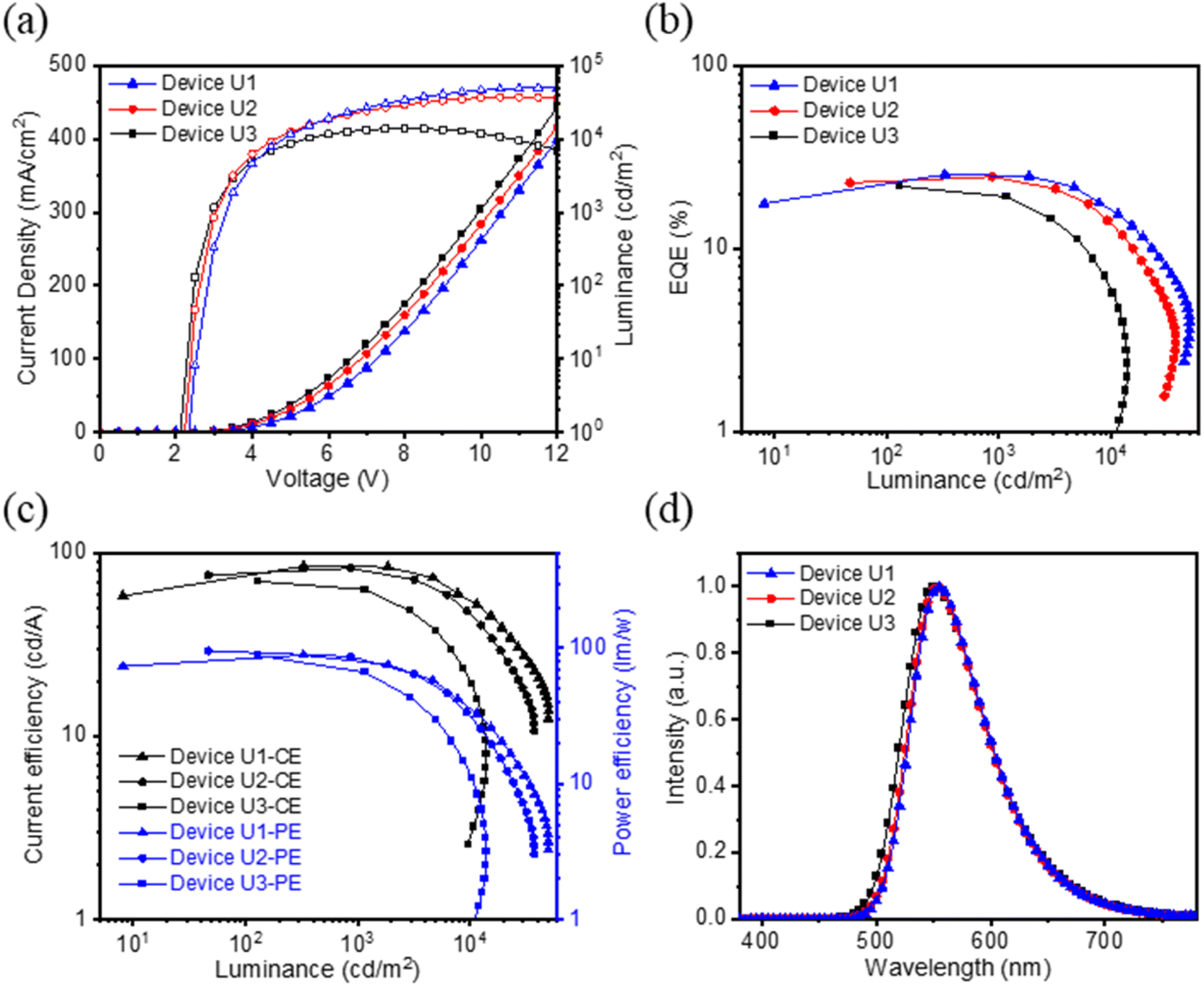 | ||
| Fig. 5 Ultrathin EML devices U1, U2, and U3: (a) Current density and luminance versus voltage plot. (b) EQE versus luminance plot. (c) CE and power efficiency PE versus luminance. (d) Electroluminescence spectra at 8 V. | ||
| Devicea | EML Thickness [nm]a | V d [V]b | η EQE,max [%]c | η CE,max [cd A−1]d | η PE,max [lm W−1]e | η EL [nm]f | CIE [x, y]g |
|---|---|---|---|---|---|---|---|
| a Device configuration: ITO/TAPC (50 nm)/TCTA (10 nm)/tBuCzDBA (1–10 nm)/B4PYMPM (65 nm)/LiF (1 nm)/Al (100 nm). b The operating voltage at a brightness of 1 cd m−2. c EQE, maximum external quantum efficiency. d CE, maximum current efficiency. e PE, maximum power efficiency. f The EL emission peak at 8 V. g CIE 1931 coordinates. | |||||||
| U1 | 10 | 2.3 | 25.5 | 85.0 | 89.0 | 555 | (0.44, 0.55) |
| U2 | 5 | 2.2 | 24.5 | 82.9 | 95.3 | 553 | (0.38, 0.59) |
| U3 | 1 | 2.1 | 22.0 | 70.2 | 88.2 | 552 | (0.44, 0.55) |
Conclusion
In summary, the concept of engineering molecules with high horizontal orientation in neat films was demonstrated in this study. By adding bulky substituents at favorable positions, tBuCzDBA not only exhibits a low degree of ACQ effect but also increases the horizontally oriented emitting dipole in pristine films. The excellent nondoped device without any doping layer achieved an EQE of 26.9% by using tBuCzDBA as the EML material. Furthermore, ultrathin EML (1 nm) OLEDs exhibited a very low turn-on voltage (2.1 V) and maintained a high efficiency (22.0%). It is worth noting that device U2 achieved the highest power efficiency of 95.3 lm W−1, indicating the achievement of both energy-saving and low-cost fabrication. We believe that this material design of molecules with a high horizontal ratio and reduced ACQ effect in neat films offers a new perspective for low power/cost consumption OLEDs in the future.Experimental section
Theoretical calculation
All quantum chemical simulations were performed using the Gaussian 16 program package. The excited states of D-A-D-type molecules are sensitive to functionals,44 several functionals including B3LYP, CAMB3LYP, PBE0, BMK, M06-2X, and ωB97XD are selected to evaluate the singlet (S1) and triplet (T1) excited energies with the 6-31G* basis set (Table S2†). The calculated S1 and T1 energy levels with the BMK functional are in good agreement with the experimental values. All density-functional theory (DFT)/time-dependent (TD) DFT calculations were all carried out on the basis of BMK/6-31G*. TD-DFT was then used to obtain the vertical transitions of the lowest-lying singlet and triplet states and visualized on the Gaussview 6.0 software.Molecular dynamics
Molecular orientation for amorphous crystalline structures can be expressed as a distribution or in averaged order parameter.45 Here, stereographic projections were utilized to demonstrate the distribution of preferred orientations. Each simulation system of the three DBA molecules consists of approximately 100 molecules packed roughly neatly in a cubic unit. All NEMD simulations were performed using LAMMPS46 and the Dreiding forcefield.47 Periodic boundary conditions were used in all simulations (Fig. S11†). The time step equaled 1 fs for deposition and equilibrium after deposition. The Nose−Hoover method was used to maintain a constant temperature of 600 K for deposition. Then, all MD simulations were used for at least 1000 ps of equilibration to obtain atom position results for calculating orientation at 300 K. All setups for molecular simulations can be found in Table S3.†Photophysical measurement
UV-vis spectra were taken using a spectrophotometer (U-3300 model, Hitachi), while the steady-state fluorescence (room temp.) spectra were measured by using a PL spectrophotometer (F-7000, Hitachi). Transient PL and time-dependent emission spectra were obtained using a spectrometer (FLS980, Edinburgh Inst). The HOMO levels of iCzDBA in neat films were determined by using a photoelectron spectrometer (AC-2, Riken Keiki) in air. The horizontal ratio of thin films was determined via the variable-angle PL measurements.20,48Device fabrication
The devices were fabricated by using a thermal evaporator on a clean ITO glass with 30 Ω per square under 10−6 torr. The deposition rate for organic materials and aluminum layer was around 0.1–0.2 nm s−1 and 0.3–0.4 nm s−1, respectively. And the rate for lithium fluoride was 0.005–0.01 nm s−1. The effective emitting area of the devices was 9.00 mm2. Current, voltage, and luminance (I–V–L) were recorded simultaneously using a Keithley 2400 source meter and a CS2000A Konica Minolta spectroradiometer. The hole-only device was made from ITO/MoO3 (1 nm)/tBuCzDBA (1 or 15 nm)/MoO3 (10 nm)/Al (100 nm), and the electron-only device was composed of ITO/Ca (5 nm)/tBuCzDBA (1 or 15 nm)/LiF (1 nm)/Al (100 nm). EQEs and PEs were calibrated using the Lambertian distributions (Fig. S15b†). All devices were encapsulated in a glove box and the measurements were performed at room temperature.Data availability
All supporting data are provided in the ESI†.Author contributions
T.-L. W. and C.-H. C. contributed to the manuscript writing and funding acquisition. T.-L. W. mainly contributed to the conceptualization, project administration, visualization, and investigation of material synthesis. J. L. contributed to the writing and investigation of theoretical calculations. C.-M. H., Y.-K. C., and P.-Y. H. contributed to the investigation of device fabrication and measurement. P.-T. L. executed the measurement of spectroscopic ellipsometry. T.-Y. C. contributed to the investigation of emitting dipole orientations. W.-C. L. and W. C. contributed to the investigation and methodology of molecular dynamics simulations. C.-H. Y., L.-Y. H., and H.-W. L. performed the supervision and formal analysis. All authors discussed the progress of research and reviewed the manuscript.Conflicts of interest
The authors declare no conflict of interest.Acknowledgements
We thank the National Science and Technology Council of Taiwan (NSTC 110-2113-M-007-008; 110-2113-M-007-028-MY3) and the Frontier Research Center on Fundamental and Applied Sciences of Matters by the Ministry of Education (NSTC 110-2634-F-007-023) for support of this research. We also thank the National Center for High-Performance Computing (Account number: u32chc04) of Taiwan for providing the computing time and assistance in experiments at the Instrumentation Center of Taiwan (NSTC 110-2731-M-007-001). T.-L. W. acknowledges the synthetic support from Yu-Che Chang and acknowledges the support of the Yushan Young Scholar Program by the Ministry of Education, Taiwan.References
- H. Uoyama, K. Goushi, K. Shizu, H. Nomura and C. Adachi, Nature, 2012, 492, 234–238 CrossRef CAS PubMed
.
- K. H. Kim and J. J. Kim, Adv. Mater., 2018, 30, 1705600 CrossRef PubMed
- K. Goushi, K. Yoshida, K. Sato and C. Adachi, Nat. Photonics, 2012, 6, 253–258 CrossRef CAS
- M. Y. Wong and E. Zysman-Colman, Adv. Mater., 2017, 29, 1605444 CrossRef PubMed
- H. Kaji, H. Suzuki, T. Fukushima, K. Shizu, K. Suzuki, S. Kubo, T. Komino, H. Oiwa, F. Suzuki, A. Wakamiya, Y. Murata and C. Adachi, Nat. Commun., 2015, 6, 8476 CrossRef CAS
- Y. K. Chen, J. Jayakumar, C. M. Hsieh, T. L. Wu, C. C. Liao, J. Pandidurai, C. L. Ko, W. Y. Hung and C. H. Cheng, Adv. Mater., 2021, 33, 2008032 CrossRef CAS PubMed
- D. Yokoyama, J. Mater. Chem., 2011, 21, 19187–19202 RSC
- C. Y. Chan, M. Tanaka, Y. T. Lee, Y. W. Wong, H. Nakanotani, T. Hatakeyama and C. Adachi, Nat. Photon., 2021, 15, 203–207 CrossRef CAS
- T. Komino, Y. Sagara, H. Tanaka, Y. Oki, N. Nakamura, H. Fujimoto and C. Adachi, Appl. Phys. Lett., 2016, 108, 241106 CrossRef
- D. D. Zhang, C. G. Zhao, Y. G. Zhang, X. Z. Song, P. C. Wei, M. H. Cai and L. Duan, ACS Appl. Mater. Interfaces, 2017, 9, 4769–4777 CrossRef CAS PubMed
- J. Lee, N. Aizawa, M. Numata, C. Adachi and T. Yasuda, Adv. Mater., 2017, 29, 1604856 CrossRef PubMed
- J. Guo, X.-L. Li, H. Nie, W. Luo, S. Gan, S. Hu, R. Hu, A. Qin, Z. Zhao, S.-J. Su and B. Z. Tang, Adv. Funct. Mater., 2017, 27, 1606458 CrossRef
- H. J. Liu, J. J. Zeng, J. J. Guo, H. Nie, Z. J. Zhao and B. Z. Tang, Angew. Chem., Int. Ed., 2018, 57, 9290–9294 CrossRef CAS
- K. C. Wu, P. J. Ku, C. S. Lin, H. T. Shih, F. I. Wu, M. J. Huang, J. J. Lin, I. C. Chen and C. H. Cheng, Adv. Funct. Mater., 2008, 18, 67–75 CrossRef CAS
- K. Matsuo and T. Yasuda, Chem. Sci., 2019, 10, 10687–10697 RSC
- T. Xu, J. G. Zhou, C. C. Huang, L. Zhang, M. K. Fung, I. Murtaza, H. Meng and L. S. Liao, ACS Appl. Mater. Interfaces, 2017, 9, 10955–10962 CrossRef CAS
- Y. B. Zhao, J. S. Chen and D. G. Ma, ACS Appl. Mater. Interfaces, 2013, 5, 965–971 CrossRef CAS
- L. P. Zhu, Y. B. Zhao, H. M. Zhang, J. S. Chen and D. G. Ma, J. Appl. Phys., 2014, 115, 244512 CrossRef
- T. M. Zhang, C. S. Shi, C. Y. Zhao, Z. B. Wu, J. S. Chen, Z. Y. Xie and D. G. Ma, ACS Appl. Mater. Interfaces, 2018, 10, 8148–8154 CrossRef CAS PubMed
- T.-L. Wu, M.-J. Huang, C.-C. Lin, P.-Y. Huang, T.-Y. Chou, R.-W. Chen-Cheng, H.-W. Lin, R.-S. Liu and C.-H. Cheng, Nat. Photon., 2018, 12, 235–240 CrossRef CAS
- N. B. Kotadiya, P. W. M. Blom and G. J. A. H. Wetzelaer, Nat. Photon., 2019, 13, 765–769 CrossRef CAS
- Y. Li, N. B. Kotadiya, B. van der Zee, P. W. M. Blom and G. J. A. H. Wetzelaer, Adv. Opt. Mater, 2021, 9, 2001812 CrossRef CAS
- K. H. Kim, J. Y. Baek, C. W. Cheon, C. K. Moon, B. Sim, M. Y. Choi, J. J. Kim and Y. H. Kim, Chem. Commun., 2016, 52, 10956–10959 RSC
- X. L. Chen, J. H. Jia, R. M. Yu, J. Z. Liao, M. X. Yang and C. Z. Lu, Angew. Chem., Int. Ed., 2017, 56, 15006–15009 CrossRef CAS PubMed
- Q. S. Zhang, D. Tsang, H. Kuwabara, Y. Hatae, B. Li, T. Takahashi, S. Y. Lee, T. Yasuda and C. Adachi, Adv. Mater., 2015, 27, 2096–2100 CrossRef CAS PubMed
- M. Godumala, S. Choi, M. J. Cho and D. H. Choi, J. Mater. Chem. C, 2019, 7, 2172–2198 RSC
- Z. Y. Xie, C. Cao, Y. Zou, X. S. Cao, C. J. Zhou, J. W. He, C. S. Lee and C. L. Yang, Adv. Funct. Mater., 2022, 32, 2112881 CrossRef CAS
- C. Hoffend, F. Schodel, M. Bolte, H. W. Lerner and M. Wagner, Chem. Eur. J., 2012, 18, 15394–15405 CrossRef CAS PubMed
- A. C. Benniston, A. Harriman, S. L. Howell, C. A. Sams and Y. G. Zhi, Chem. Eur. J., 2007, 13, 4665–4674 CrossRef CAS PubMed
- F. B. Dias, T. J. Penfold and A. P. Monkman, Methods Appl. Fluoresc., 2017, 5, 012001 CrossRef PubMed
- J. Huang, H. Nie, J. J. Zeng, Z. Y. Zhuang, S. F. Gan, Y. J. Cai, J. J. Guo, S. J. Su, Z. J. Zhao and B. Z. Tang, Angew. Chem., Int. Ed., 2017, 56, 12971–12976 CrossRef CAS PubMed
- S. Y. Byeon, J. Kim, D. R. Lee, S. H. Han, S. R. Forrest and J. Y. Lee, Adv. Opt. Mater., 2018, 6, 1701340 CrossRef
- K. H. Kim, J. Y. Baek, C. W. Cheon, C. K. Moon, B. Sim, M. Y. Choi, J. J. Kim and Y. H. Kim, Chem. Commun., 2016, 52, 10956–10959 RSC
- D. H. Kim, K. Inada, L. Zhao, T. Komino, N. Matsumoto, J. C. Ribierre and C. Adachi, J. Mater. Chem. C, 2017, 5, 1216–1223 RSC
- K. H. Kim, J. L. Liao, S. W. Lee, B. Sim, C. K. Moon, G. H. Lee, H. J. Kim, Y. Chi and J. J. Kim, Adv. Mater., 2016, 28, 2526–2532 CrossRef CAS
- R. Furue, T. Nishimoto, I. S. Park, J. Lee and T. Yasuda, Angew. Chem., Int. Ed., 2016, 55, 7171–7175 CrossRef CAS
- L. Yu, Z. B. Wu, G. H. Xie, W. X. Zeng, D. G. Ma and C. L. Yang, Chem. Sci., 2018, 9, 1385–1391 RSC
- I. S. Park, K. Matsuo, N. Aizawa and T. Yasuda, Adv. Funct. Mater., 2018, 28, 1802031 CrossRef
- J. Lee, N. Aizawa and T. Yasuda, Chem. Mater., 2017, 29, 8012–8020 CrossRef CAS
- I. S. Park, K. Matsuo, N. Aizawa and T. Yasuda, Adv. Funct. Mater., 2018, 28, 1802031 CrossRef
- J. J. Guo, X. L. Li, H. Nie, W. W. Luo, R. R. Hu, A. J. Qin, Z. J. Zhao, S. J. Su and B. Z. Tang, Chem. Mater., 2017, 29, 3623–3631 CrossRef CAS
- F. Rizzo and F. Cucinotta, Isr. J. Chem., 2018, 58, 874–888 CrossRef CAS
- H. J. Liu, H. Liu, J. Z. Fan, J. J. Guo, J. J. Zeng, F. L. Qiu, Z. J. Zhao and B. Z. Tang, Adv. Opt. Mater., 2020, 8, 2001027 CrossRef CAS
- J. L. Bredas, Chem. Mater., 2017, 29, 477–478 CrossRef CAS
- S. Shikita, G. Watanabe, D. Kanouchi, J. Saito and T. Yasuda, Adv. Photonics Res., 2021, 2, 2100021 CrossRef
- A. P. Thompson, H. M. Aktulga, R. Berger, D. S. Bolintineanu, W. M. Brown, P. S. Crozier, P. J. I. Veld, A. Kohlmeyer, S. G. Moore, T. D. Nguyen, R. Shan, M. J. Stevens, J. Tranchida, C. Trott and S. J. Plimpton, Comput. Phys. Commun., 2022, 271, 108171 CrossRef CAS
- S. L. Mayo, B. D. Olafson and W. A. Goddard, J. Phys. Chem., 1990, 94, 8897–8909 CrossRef CAS
- K. T. Ly, R. W. Chen-Cheng, H. W. Lin, Y. J. Shiau, S. H. Liu, P. T. Chou, C. S. Tsao, Y. C. Huang and Y. Chi, Nat. Photonics, 2017, 11, 63–68 CrossRef
Footnote |
| † Electronic supplementary information (ESI) available. CCDC 1515214, 2210541 and 2210542. For ESI and crystallographic data in CIF or other electronic format see DOI: https://doi.org/10.1039/d2sc04725j |
| This journal is © The Royal Society of Chemistry 2022 |