
 Open Access Article
 This Open Access Article is licensed under a Creative Commons Attribution-Non Commercial 3.0 Unported Licence
Interpretation of Mott–Schottky plots of photoanodes for water splitting†
Sandheep
Ravishankar
 *a,
Juan
Bisquert
b and
Thomas
Kirchartz
ac
*a,
Juan
Bisquert
b and
Thomas
Kirchartz
ac
aIEK-5 Photovoltaik, Forschungszentrum Jülich, 52425 Jülich, Germany. E-mail: s.ravi.shankar@fz-juelich.de
bInstitute of Advanced Materials, Universitat Jaume I, Castellón de la Plana 12071, Spain
cFaculty of Engineering and CENIDE, University of Duisburg-Essen, Carl-Benz-Str. 199, 47057 Duisburg, Germany
First published on 31st March 2022
Abstract
A large body of literature reports that both bismuth vanadate and haematite photoanodes are semiconductors with an extremely high doping density between 1018 and 1021 cm−3. Such values are obtained from Mott–Schottky plots by assuming that the measured capacitance is dominated by the capacitance of the depletion layer formed by the doping density within the photoanode. In this work, we show that such an assumption is erroneous in many cases because the injection of electrons from the collecting contact creates a ubiquitous capacitance step that is very difficult to distinguish from that of the depletion layer. Based on this reasoning, we derive an analytical resolution limit that is independent of the assumed active area and surface roughness of the photoanode, below which doping densities cannot be measured in a capacitance measurement. We find that the reported doping densities in the literature lie very close to this value and therefore conclude that there is no credible evidence from capacitance measurements that confirms that bismuth vanadate and haematite photoanodes contain high doping densities.
Introduction
Bismuth vanadate (BiVO4) and haematite (α-Fe2O3) semiconductor films have been intensely studied over the last two decades as viable photoanodes for efficient solar water oxidation. Such investigations have mainly involved design and material modifications, such as nanostructuring,1–3 addition of charge selective or passivating layers,4–7 doping,8,9 thermal treatments that alter their bulk and surface properties,10,11 and the use of catalysts12–14 that maximise charge transfer from the photoanode to the electrolyte. However, while the photoconversion efficiencies of these devices have improved significantly, a deeper understanding of their physics of operation is still lacking. This is because of the limitations of the interpretative framework used to analyse the results of commonly-used characterization techniques such as impedance spectroscopy (IS), intensity-modulated photocurrent spectroscopy (IMPS) and Mott–Schottky analysis (C−2vs. V, where C is the capacitance and V is the applied voltage). The interpretation of IS spectra is difficult because it requires assuming an equivalent circuit that can sometimes be quite complex and yields resistances and capacitances whose experimental evolution deviates significantly from theoretical predictions,7,15–17 while IMPS spectra are interpreted using the evolution of time constants18,19 based on a kinetic model whose validity has been questioned.20 In the case of Mott–Schottky analysis, a large body of literature reports very high doping densities in these photoanodes between 1018 and 1021 cm−3 both before and after material modification, which suggests that the BiVO4 and Fe2O3 used in these devices are degenerate semiconductors.21–24The uncertainty with regard to the Mott–Schottky analysis is particularly troubling because it implies a certain physics of operation. Since the photoanode is operated at large anodic (reverse) bias, the electric field is an important factor controlling its performance, driving electrons to the collecting contact and holes to the photoanode/electrolyte interface for subsequent transfer to the electrolyte. Such large doping densities suggest that the depletion region is substantially thinner than the photoanode at the operating voltage and the holes generated closer to the collecting contact are required to diffuse over a distance before being collected by the electric field. In such cases, bulk transport limitations can also limit the performance in addition to the more well-known slow kinetics/recombination at the photoanode/electrolyte interface.18,22,25–28 Several publications have indeed questioned the interpretation of these Mott–Schottky plots and discussed the different situations under which the Mott–Schottky equation and its corresponding assumptions cannot be directly applied. Hankin et al.29 have discussed the importance of accounting for the distribution of the applied external potential across both the depletion layer and the Helmholtz layer, especially in situations of large doping densities. Peter et al.30 showed that the planar capacitance formula used to derive the Mott–Schottky equation is invalid for nanostructured photoanodes with spherical and cylindrical geometries especially at deep reverse (anodic) bias, where the depletion layer width deviates strongly from the  proportionality. The maximum potential drop through the individual nanostructures is also limited by their geometry, as shown by Bisquert.31 For nanoporous films, an additional consideration is that the electrolyte can penetrate through the thickness of the photoanode, allowing the ions in the electrolyte to shield the electric field31 and the electrostatic potential drop to occur mainly between the substrate and the electrolyte, rather than the substrate and the nanoporous film. In fact, Fabregat-Santiago et al. showed that Mott–Schottky measurements of fluorine-doped tin oxide (FTO) substrates covered by nanoporous titanium-dioxide (TiO2) films are dominated by the capacitance of the FTO substrate rather than the TiO2 film.32
Whilst all these factors are important, the most fundamental requirement for detecting a doping or trap density in a capacitance measurement is that it needs to sufficiently affect the electrostatic potential to create a space-charge region shorter than the thickness of the semiconductor. If this does not happen, the electric field in the device remains unaffected and the charge density cannot be detected. In this work, we use this argument to determine resolution limits for the detection of charge densities of bismuth vanadate and haematite photoanodes in a capacitance measurement, previously derived in ref. 33. This resolution limit serves as an upper limit of doping/trap densities in the material and is a function of the permittivity and thickness of the material, while being independent of the assumed active area. By analysing reported Mott–Schottky plots of haematite and bismuth vanadate photoanodes, we identify that all the reported doping/trap densities are very close to the resolution limit, indicating that they cannot credibly be assigned as actual doping densities. For any Mott–Schottky measurements in the future, we suggest that the calculated doping density be compared to the resolution limit and only if it is significantly higher than the limit, be considered an actual doping density. If not, then the value serves only as an upper limit to the actual doping density in the photoanode. Based on these results, we propose alternative band diagrams of the photoanode in different bias situations (from drift-diffusion simulations using SCAPS – a Solar Cell Capacitance Simulator)34 with a fairly constant electric field throughout the whole photoanode, as opposed to the widely-accepted picture of a sharp potential drop at the photoanode/electrolyte interface and a field-free bulk.
Results and discussion
Before analysing reported data, we first provide a brief overview of the underlying physics that allows the determination of dopant or trap densities in a Mott–Schottky plot. Fig. 1(a) shows the simulated band diagram of a photoanode of thickness d at equilibrium (simulation details and parameters shown in Table S1 in the ESI†). An electrostatic built-in potential difference Vbi is formed at the photoanode/electrolyte interface. The associated depletion region extends into the photoanode over a distance w. As shown in Fig. 1(b), this region is assumed to be depleted of majority carriers (hence called depletion region), with the net electrostatic potential being determined only by the density of charged dopant/trap species. In the region beyond the depletion region (x < w), the charge of the dopant/traps is counterbalanced by an equal density of majority carriers (in this case, electrons), leading to zero net charge and zero electrostatic potential drop, hence termed the neutral region. The depletion region can be considered a parallel-plate capacitor with capacitance | (1) |
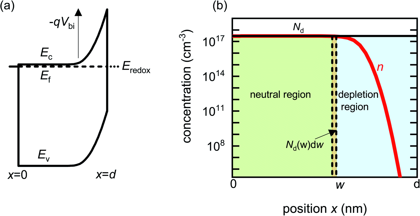 | ||
| Fig. 1 (a) Simulated band diagram of a photoanode at equilibrium. The collecting contact is at x = 0 and the photoanode/electrolyte interface is at x = d. Vbi is the built-in potential difference. (b) Carrier concentration as a function of position in a photoanode with constant doping density Nd = 3 × 1017 cm−3. When a small voltage perturbation is applied, a charge density Nd(w) × dw is swept out from the edge of the depletion region of width w (yellow region). Simulation parameters are provided in Table S1 in the ESI.† | ||
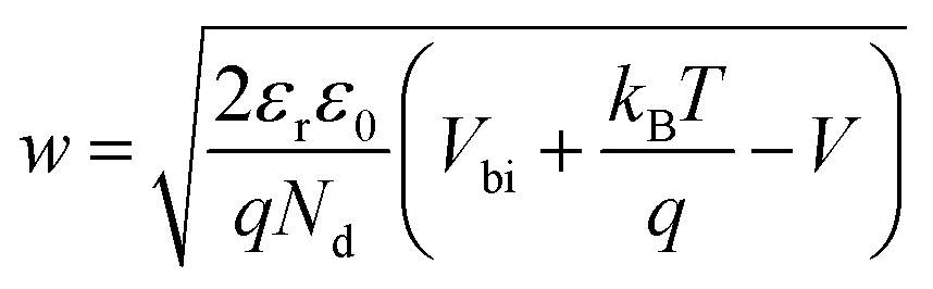
The solution of the Poisson equation yields the width of the depletion region as35
 | (2) |
The application of a cathodic (forward) voltage reduces the electrostatic potential drop (i.e. Vbi − V becomes smaller) in the space-charge region, while an anodic (reverse) voltage increases it. Upon the application of a small perturbation of voltage, the width of the depletion region is altered by a factor dw from its steady-state value w and a charge density Nd(w) × dw is swept out from the edge of the depletion region (Fig. 1 shows a constant doping density for simplicity but in general, the doping density is variable along the thickness of the photoanode), which manifests itself as the measured current.36Eqn (2) implies that at deep anodic (reverse) bias, the entire thickness of the semiconductor is depleted (w = d) and the capacitance saturates at the geometric capacitance, given by
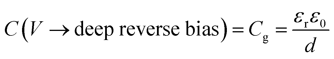 | (3) |
From eqn (1) and (2), we obtain36
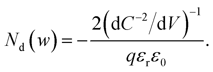 | (4) |
Eqn (4) implies that the inverse slope of the Mott–Schottky plot at a given voltage is proportional to the doping density at the edge of the depletion region width w at the same voltage. Therefore, eqn (4) can be plotted against w = εrε0/C(V) (termed the ‘profiling distance’) (eqn (1)) to determine the spatial distribution of dopant/trap densities in the photoanode (termed a ‘doping profile’ plot. Examples of doping profiles are provided in ref. 33). An alternate practice commonly used in the solar fuel community is to fit a straight line through the C−2vs. V data to obtain an average dopant/trap density. The intercept of this line on the V axis also allows determining the flatband potential Vfb, corresponding to the region of capacitance saturation at large cathodic bias.
The correct application and analysis of the Mott–Schottky method requires acknowledging some fundamental resolution limits inherent to it, based on simple electrostatics. For a density of charge to be detected in a capacitance measurement, it must affect the electrostatic potential sufficiently. In the case of a non-porous semiconductor layer of thickness d sandwiched between two electrodes, this charge density must then be significantly larger than the surface charge density σ on the electrodes. This leads to the condition37
| qNdd > σ | (5) |
The subsequent question that arises based on the discussion so far is: in situations where the doping/trap density does not affect the capacitance, what generates the capacitance step in a Mott–Schottky plot that is ubiquitously observed? In order to answer this question, it is important to first establish what a forward and reverse bias is for the photoanode. The definition of a forward bias is unclear since the applied voltage at the collecting contact is referenced to an external redox potential (three-electrode configuration), usually a Ag/AgCl electrode. This means that the voltage applied to the absorber layer is unknown since we do not have access to the hole Fermi level from the electrolyte side via a metal contact (see Fig. 1(a)). However, we can define a forward bias using the relative change in the electron Fermi level position (that we have access to from the collecting contact side) from an equilibrium to a non-equilibrium steady-state situation by assuming that the hole Fermi level at the absorber/electrolyte interface (i.e. at x = d in Fig. 1(a)) is pinned to the redox level of the electrolyte. Thus, for a Mott–Schottky measurement, we have the total forward bias as
| Vforward = VOCP, dark − V | (6) |
| Vmax, MS = VOCP, dark − VFB, app | (7) |
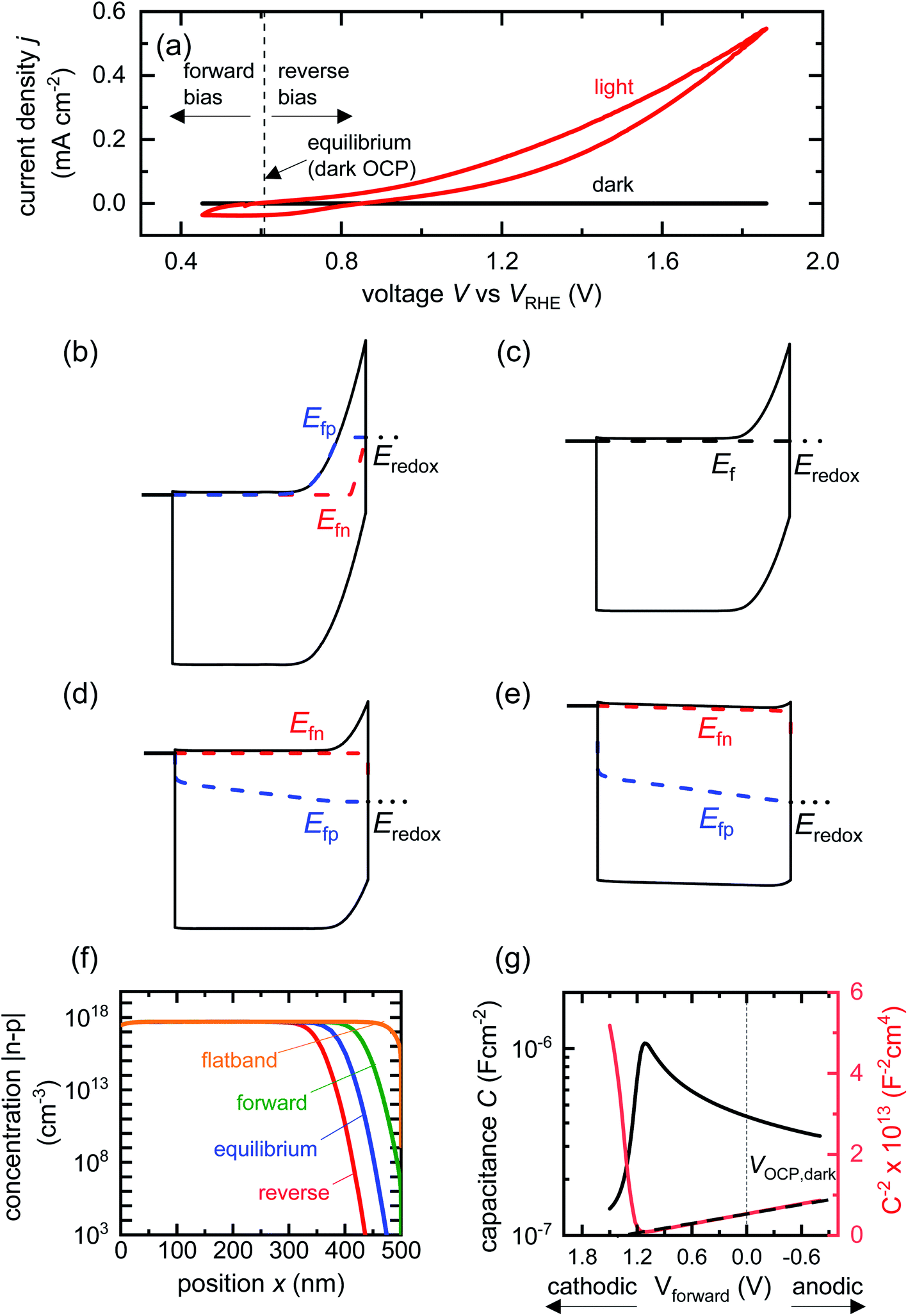 | ||
| Fig. 2 (a) Cyclic voltammetry curves of a BiVO4 photoanode in the dark and under one sun illumination. Also shown are the voltages corresponding to large forward bias, equilibrium (dark open-circuit potential) and deep reverse bias (anodic voltages). Simulated band diagrams of a doped BiVO4 photoanode (Nd = 5 × 1017 cm−3) in the dark at (b) reverse bias, (c) equilibrium, (d) forward bias and (e) flatband conditions. (f) Shows the net concentration |n–p| in the photoanode as a function of position for the different bias situations in (b)–(e). The net concentration is dominated by the electron density, which is several orders of magnitude larger than the hole density in all cases. (g) Capacitance step and corresponding Mott–Schottky plot (dashed line shows linear Mott–Schottky region) from a simulated small-perturbation capacitance–voltage measurement (103 Hz). This capacitance corresponds to the depletion capacitance. Simulation parameters are shown in Table S2 in the ESI.† | ||
We now proceed to discuss the origin of the capacitance step observed in a Mott–Schottky measurement. Fig. 2(b)–(e) show simulated band diagrams (by numerically solving the drift-diffusion equations, see Section A1 for description of simulations and Section A2 for discussion of parameters in the ESI†) of a doped photoanode in the dark under different bias conditions, from reverse bias to equilibrium, then forward bias and ultimately flatband. We note that the simulations are shown using the same potential scale defined in eqn (6), where the dark open-circuit potential is zero volts since no reference electrode is considered for the simulations. Due to the large doping density in the photoanode, there is a sharp potential drop at the photoanode/electrolyte interface, creating a small depletion layer and a large neutral region. This depletion region is eventually reduced in width and ultimately removed upon application of a forward bias. The corresponding change in net charge density (in this case, electron density, since the hole density is several orders of magnitude lower) is shown in Fig. 2(f). The simulated capacitance–voltage behaviour and the corresponding Mott–Schottky plot are shown in Fig. 2(g). The upward step in capacitance moving from anodic to cathodic voltage creates a linear Mott–Schottky region (dashed lines in Fig. 2(g)), as expected for a depletion capacitance. While the capacitance behaviour is obtained from a simulated small-perturbation capacitance–voltage measurement, we find that the ratio of the differential steady-state net charge density and differential voltage (i.e. C = dQ/dV) provides an accurate estimation of the capacitance obtained from the small-perturbation measurement (see Fig. S1(a) in the ESI†).
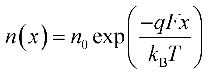
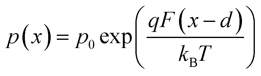
We now consider an undoped (intrinsic) photoanode, whose band diagrams corresponding to different bias situations in the dark are shown in Fig. 3(a)–(d). These situations are identical to that in Fig. 2(b)–(e) except for the fact that there is no depletion layer in the photoanode. Instead, there is a constant electric field through the thickness of the semiconductor at equilibrium, determined by the difference between the electron contact work function and the energetic distance of the redox level from the surface vacuum level. Upon applying a forward bias, the electric field and the tilting of the bands are reduced. This is the situation shown in Fig. 3(c) where the electric field is smaller compared to Fig. 3(b). Upon applying a larger forward bias, the electric field nearly vanishes and the flatband condition shown in Fig. 3(d) is reached. An undoped photoanode also shows a large increase in net charge density through its thickness upon the application of a forward bias, shown in Fig. 3(e), resulting in the capacitance step in Fig. 3(f) (the differential capacitance calculated from the steady-state net charge density in Fig. 3(e) provides a good approximation of the capacitance, see Fig. S1(b) in the ESI†). We note that in the case of the undoped photoanode, the injected charge that causes the capacitance step is that of the majority carriers (electrons) and not the minority carriers (holes). This occurs due to the difference in injection barriers for electrons and holes at the electron-contact/photoanode interface and photoanode/electrolyte interface, 0.05 eV and 1.05 eV respectively (see Table S3 in the ESI†). Therefore, the equilibrium concentrations for electrons and holes at the electron-contact/photoanode and photoanode/electrolyte interfaces respectively are n0 = 2.9 × 1017 cm−3 and p0 = 5.78 cm−3. The electron and hole concentrations along the length of the photoanode at equilibrium is then given by
 | (8) |
 | (9) |
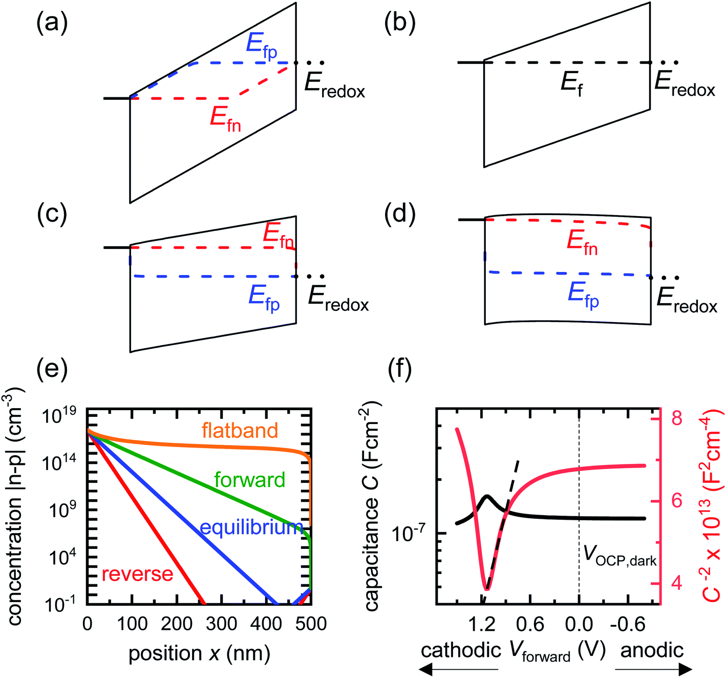 | ||
| Fig. 3 Simulated band diagrams of an undoped (intrinsic) photoanode in the dark at (a) deep reverse bias, (b) equilibrium, (c) forward bias and (d) flatband conditions. (e) Shows the corresponding total concentration |n–p| as a function of position in the photoanode for the different situations in (a)–(d). The hole density is several orders lower in magnitude than that of the electrons in all cases, which means the total charge density in the device is dominated by the electron density (majority carriers). (f) Shows the capacitance step and corresponding Mott–Schottky plot and apparent flatband potential from a simulated small-perturbation capacitance–voltage measurement (103 Hz). Simulation parameters are shown in Table S3 in the ESI.† | ||
The electric field F is given by
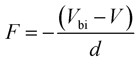 | (10) |
We have so far considered two extreme cases, the first one being a highly-doped semiconductor where the capacitance response is dominated by the depletion capacitance (Fig. 2) and the second one being an undoped, intrinsic photoanode where the capacitance response is dominated by the electrochemical capacitance (Fig. 3). However, there are several reports in literature suggesting the presence of a background doping density in these photoanodes, arising from oxygen vacancies and hydrogen donors in the case of bismuth vanadate40–42 and oxygen vacancies in the case of haematite.43–45 We therefore simulate an intermediate case where a doping density exists in the photoanode but the capacitance step is still dominated by the electrochemical capacitance (see Fig. S3†). In this scenario, the doping density is not high enough to modify the electrostatic potential and create a depletion region, which leads to a similar situation as the undoped case in Fig. 3. Thus, the electrochemical capacitance can dominate the total capacitance response even in situations where a doping density is present in the photoanode. Additionally, since capacitance measurements rely on the amount of charge placed on the dopants (that create the depletion region and the subsequent capacitance response), positively-charged and negatively-charged dopants can cancel each other out and remain invisible in these methods. To provide an intuitive understanding of the capacitance step generated by the injection of electrons from the electron contact, we show a schematic of the process in Fig. 4.
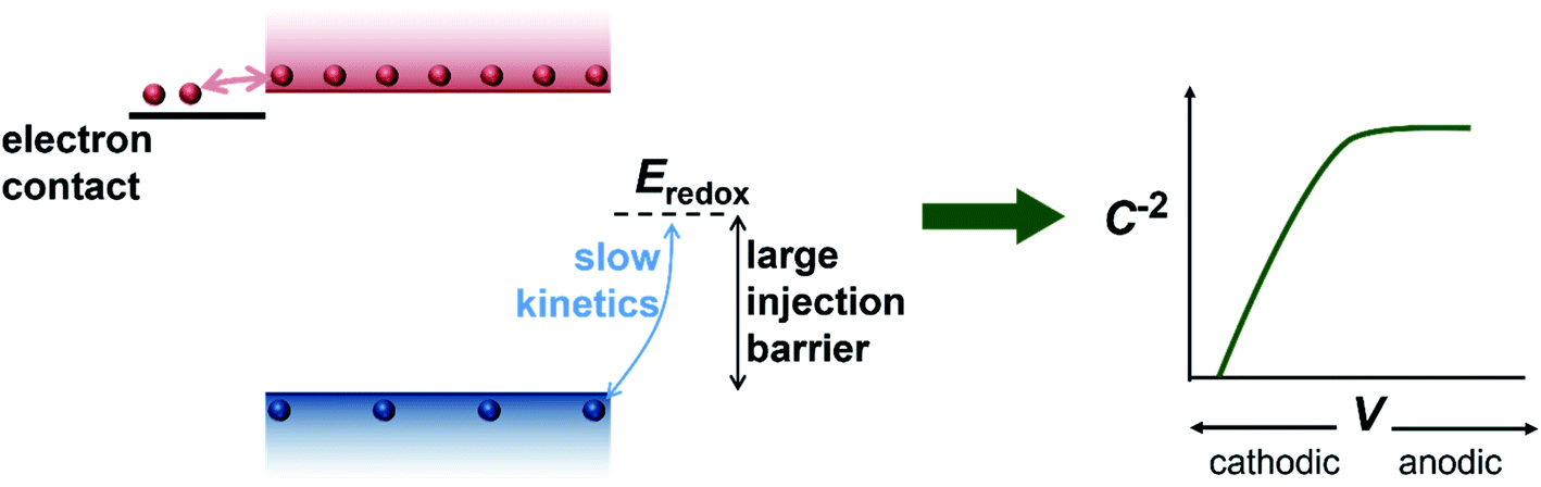 | ||
| Fig. 4 Schematic of the process of injection of electrons (red spheres) from the electron contact into the photoanode that generates the capacitance step in the dark and consequent Mott–Schottky plot observed experimentally. The hole density (blue spheres) in the photoanode is very low due to the large injection barrier at the photoanode/electrolyte interface, causing the electrons to dominate the capacitance step. | ||
To identify if the capacitance associated to injection of electrons from the metal contact is indeed a significant factor affecting the Mott–Schottky measurements, we calculate the magnitude of forward bias used in typical Mott–Schottky measurements of bismuth vanadate and haematite photoanodes reported in literature, shown in Fig. 5(a). This figure shows that most of the Mott–Schottky plots are measured under at least a few hundred mV of forward bias, indicating that charge injection is a process that can significantly affect the capacitance response in a Mott–Schottky measurement.
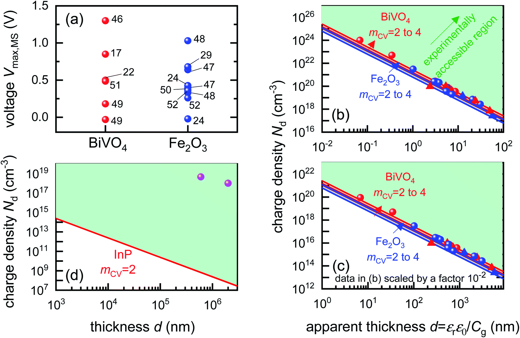 | ||
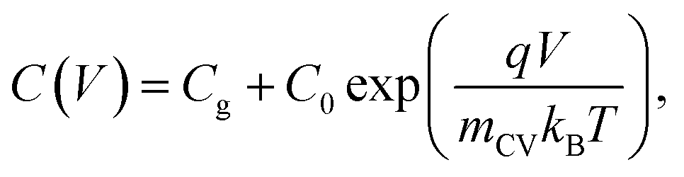
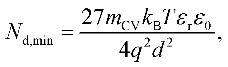
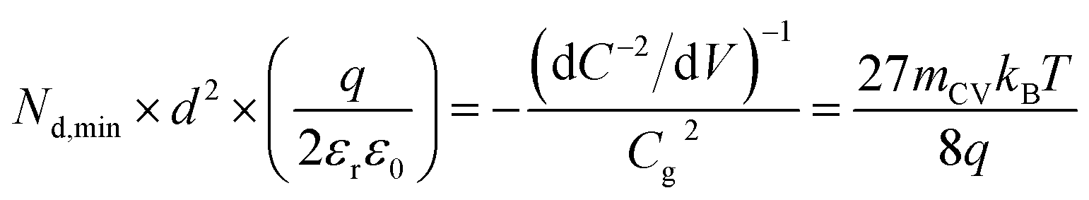
| Fig. 5 (a) Literature data points (corresponding to reference number as shown) of the maximum forward voltage applied in a Mott–Schottky measurement calculated from the difference between the dark open-circuit voltage and the flatband potential, see eqn (7). Cathodic (negative) voltages imply the exponential injection of electrons into the photoanode from the collecting contact during a Mott–Schottky measurement. (b) Doping densities of BiVO4 (red) and Fe2O3 (blue) photoanodes as a function of apparent device thickness, calculated from Mott–Schottky plots reported in literature. Triangles indicate data points where the capacitance saturates at deep reverse (anodic) bias. The minimum doping density resolvable from capacitance measurements for different mCV values (see eqn (12)) is also plotted. All the data points lie very close to the resolution limits and hence cannot credibly be ascribed to actual dopant densities in the device. (c) Data points in (b) plotted with the capacitance multiplied by an arbitrary factor of 10−2. The data points still remain very close to the resolution limits, indicating that the assumed active area and surface roughness factors of the device has no effect on the resolving power of the capacitance measurement. The apparent thickness was calculated from the smallest capacitance value at deep reverse (anodic) bias, see eqn (3). The data points were obtained for (a) from ref. 17, 22, 24, 29, 46–52 and for (b) from ref. 1, 2, 7, 8, 17, 21–24, 44, 47, 48, 53–55. (d) Doping densities of InP photoelectrodes as a function of reported device thickness. The doping densities were calculated from the plateau region of the doping profile, assuming a relative permittivity of εr = 12.5. The data points correspond to ref. 56 and 57, both of which are above the resolution limit corresponding to a valid doping density. The doping density values as obtained from the Mott–Schottky data are similar to the values provided by the suppliers of the InP single crystals (1–4 × 1018 cm−3 and 6.7 × 1017 cm−3 respectively). εr = 68, εr = 32 and εr = 12.5 was assumed for bismuth vanadate, haematite and indium phosphide respectively, to calculate the doping density from the plateau region of the doping profile (see Fig. S5 in the ESI†). | ||
To determine the form of this capacitance, we consider that in case of a field-free, intrinsic photoanode with symmetric injection barriers, we have n = p which gives n,p ∝ exp(qV/2kBT) while in the case of a doped layer, we have the minority carriers taking the entire voltage, yielding p ∝ exp(qV/kBT). Since the electrochemical capacitance is proportional to the injected charge density, we can describe the capacitance evolution versus voltage as
 | (11) |
 | (12) |
Eqn (12) provides the apparent doping density observed when the capacitance step versus voltage occurs solely due to the injection of electrons into the photoanode and the charges on the electrode. Therefore, Nd,min is the minimum apparent doping density that will be observed in a Mott–Schottky plot and only real doping/trap densities larger than Nd,min can be detected in a Mott–Schottky measurement. Fig. 5(b) shows reported doping/trap densities of bismuth vanadate and haematite photoanodes in literature for different thicknesses of the photoanode layer. Note that the thickness of the film is often not provided nor is it the relevant quantity in this context. The relevant effective thickness in this context is indeed the thickness derived from the capacitance plateau at large anodic (deep reverse bias) voltages using eqn (3), whose validity is assumed in a Mott–Schottky measurement. The doping/trap densities are very close to the resolution limits calculated for a capacitance step with mCV = 2–4 and follow the Nd,min ∝ d−2 proportionality in eqn (12). We note that we use an mCV factor between 2 and 4 because Fig. 3 is a case of an undoped, intrinsic photoanode with an electric field, different from both the undoped, field-free intrinsic photoanode (mCV = 2) and the doped photoanode (mCV = 1). Thus, a simple analytical form of the capacitance cannot be achieved and the mCV factor can only be obtained through fitting of the rising capacitance step generated from the simulations to eqn (11). This yields large mCV values of ∼7.2 (see Fig. S4 in the ESI†), and hence we use mCV values between 2 and 4 for the resolution limit.
Our analysis confirms that the experimental doping densities in Fig. 5(b) are artefacts from a general capacitance transition of the form of eqn (11) and serve as upper limits to the actual doping/trap densities in the material. Additionally, the magnitudes of the experimental doping/trap densities in Fig. 5(b) are very high, with most data points between 1019–1021 cm−3. Sivula58 has recently questioned the magnitude of these doping densities, noting that they are likely in excess of the density of states in the conduction/valence bands of these materials. Such large values are in part a consequence of overestimation of the capacitance per unit area due to consideration of the planar active area, instead of the much larger effective surface area of nanostructured and porous films. The surface roughness of such nanostructured capacitors has also been shown to significantly increase the measured capacitance.59 This is reflected in the apparent thickness of the device in the x-axis of Fig. 5(b), yielding film thicknesses of (in some cases) only a few nanometres or even less.
The question then arises, whether the increase of the capacitance in nanostructured materials due to high surface areas and substantial roughness will change the position of the experimental data points relative to the validity region of the method (green region in Fig. 5(b)). We might assume that the capacitances are higher than the capacitances expected for flat films with a given doping concentration by a voltage-independent factor that is a consequence of surface roughness. Hence, we would have to study the situation where the capacitance is scaled with a factor <1. We therefore multiply the capacitance data of the points in Fig. 5(b) by an arbitrary factor of 10−2 and consider the effect of this multiplication both on the apparent doping density and the apparent thickness of the film. The resulting graph is shown in Fig. 5(c), which shows that the relative position of the experimental data and the resolution limit have not changed. The only things that have changed are the absolute values of the apparent doping density and thickness. This result is a consequence of the invariance of the resolution limit with respect to any constant multiplicative factor for the capacitance. The lines in Fig. 5(b) and (c) are lines of equal Nd,min × d2 (see eqn (12)). If we rewrite eqn (12) using eqn (3) and (4), we obtain
 | (13) |
Both the numerator and denominator of the middle term in eqn (13) contain C2 terms, which means that any scaling factors arising out of poor estimation of the active area or from surface roughness cancel out to give the constant right-hand side of eqn (13). Therefore, the scaled doping densities have only moved along the Nd ∝ d2 line to lower magnitudes and corresponding larger apparent device thicknesses. Hence, our resolution limit is also still valid even with the use of the apparent device thickness calculated from the Mott–Schottky data, however close or far it may be to the actual device thickness. To further justify the validity of our developed resolution limit, we analyse two Mott–Schottky measurements of indium phosphide (InP) single crystal photoelectrodes, shown in Fig. 5(d). The data points are well above the resolution limit, corresponding to a real doping density that also closely corresponds to the values provided by the suppliers of the InP single crystals. This shows that the method is in principle working but requires the doping density to be above the detection threshold indicated in Fig. 5.
In summary, we conclude that there is no significant evidence to justify that bismuth vanadate and haematite photoanodes are as highly doped as many capacitance measurements suggest. This is due to the fact that the large reported doping densities for these photoanodes are very close to the resolution limits of the capacitance–voltage method. We suggest that any doping/trap densities measured from capacitance–voltage methods in the future must be significantly larger than the resolution limit to be safely labelled as an actual doping density. In case it is close to or below the resolution limit, it can only be considered as an upper limit to the actual doping density in the photoanode. The actual upper limit of the doping density in the material can be determined only upon accurate calculation of the effective active area and surface roughness of the device.
These results provide an alternate view of the electrostatics in the device. Fig. 6 shows simulated band diagrams of an intrinsic photoanode at equilibrium and at large anodic and cathodic potentials under illumination. In all cases, there is a constant electric field through the entire thickness of the photoanode. This field plays an important role in maximising the photocurrent by ensuring efficient separation and transport of electrons and holes from the bulk to the collecting contact and photoanode/electrolyte interface respectively. This is in sharp contrast to the commonly-assumed picture of a small depletion layer at the photoanode/electrolyte interface and a large, neutral bulk, which requires that the bulk electrons are required to diffuse over the entire neutral region to reach the collecting contact, while the bulk holes also diffuse across the neutral region until they are swept out by the electric field and subsequently transferred to the electrolyte. We note that due to the slow kinetics of charge transfer at the photoanode/electrolyte interface, a large density of holes must exist at this interface in order to sustain the photocurrent (see eqn (S4) in the ESI†) under illumination. This makes the hole Fermi level in Fig. 6(b) and (c) appear un-pinned at the photoanode/electrolyte interface, when in fact it makes a sharp jump down to the redox level at this point.
 | ||
| Fig. 6 Simulated band diagrams of an undoped photoanode at (a) dark equilibrium, (b) anodic potential under illumination and (c) cathodic potential under illumination. In all cases, an electric field exists throughout the thickness of the photoanode that sweeps electrons to the collecting contact and holes to the photoanode/electrolyte interface. The jump in the Fermi level of the holes in (b) and (c) at the photoanode/electrolyte interface is due to the slow kinetics of hole transfer from the valence band of the photoanode to the electrolyte. Simulation parameters are provided in Table S3 in the ESI.† | ||
Conclusions
We have carried out a critical analysis of the validity of the reported large doping densities between 1018–1021 cm−3 from Mott–Schottky measurements of haematite and bismuth vanadate photoanodes. We find that most of these Mott–Schottky measurements have been carried out at cathodic voltages, implying significant injection of electrons from the metal contact into the photoanode. By accounting for the capacitive contribution of these injected electrons, we developed an analytical resolution limit that is independent of the assumed active area and surface roughness of the device, below which a density of dopants cannot be detected in a capacitance measurement. We identify that all of the reported doping densities in our dataset lie very close to the resolution limit, indicating that they are not actual doping densities but artefacts arising from injection of electrons into the photoanode during a Mott–Schottky measurement. These results indicate that there is no credible evidence from capacitance measurements that confirms that bismuth vanadate and haematite photoanodes contain high doping densities. We suggest that in the future, any doping/trap densities calculated from capacitance measurements should always be compared against the resolution limit. If the charge density is much larger than the limit, it can be safely labelled a doping/trap density. If it is close to or below the resolution limit, it can only be considered as an upper limit to the actual doping/trap density in the photoanode.Based on these insights, we provide an alternate picture of the physics of operation of the photoanode, where an electric field is present throughout the thickness of the semiconductor that drives photogenerated electrons and holes from the bulk to the collecting contact and photoanode/electrolyte interface respectively, rather than a sharp potential drop at the photoanode/electrolyte interface and a large, neutral bulk region.
Data availability
MATLAB scripts for the SCAPS simulations in this paper are archived in Zenodo with the identifier DOI: 10.5281/zenodo.6413163.Author contributions
S. R. conceptualized the project, carried out all the simulations and wrote the manuscript. J. B. and T. K. contributed to reviewing and editing the manuscript.Conflicts of interest
There are no conflicts of interest to declare.Acknowledgements
S. R. thanks Dr Miguel García Tecedor for providing the cyclic voltammetry data in Fig. 2(a) and acknowledges the German Research Foundation (DFG) for the Walter-Benjamin fellowship – project number 462572437. S. R. and T. K. acknowledge funding from the Helmholtz Association via the POF-IV program. Open access publication funded by the German Research Foundation (DFG) – 491111487.References
- S. U. Khan and J. Akikusa, J. Phys. Chem. B, 1999, 103, 7184–7189 CrossRef CAS.
- B. K. Kang, G. S. Han, J. H. Baek, D. G. Lee, Y. H. Song, S. B. Kwon, I. S. Cho, H. S. Jung and D. H. Yoon, Adv. Mater. Interfaces, 2017, 4, 1700323 CrossRef.
- Q. Zeng, J. Bai, J. Li, L. Xia, K. Huang, X. Li and B. Zhou, J. Mater. Chem. A, 2015, 3, 4345–4353 CAS.
- S. Byun, B. Kim, S. Jeon and B. Shin, J. Mater. Chem. A, 2017, 5, 6905–6913 RSC.
- D. Eisenberg, H. S. Ahn and A. J. Bard, J. Am. Chem. Soc., 2014, 136, 14011–14014 CrossRef CAS PubMed.
- F. Le Formal, N. Tetreault, M. Cornuz, T. Moehl, M. Grätzel and K. Sivula, Chem. Sci., 2011, 2, 737–743 RSC.
- L. Steier, I. Herraiz-Cardona, S. Gimenez, F. Fabregat-Santiago, J. Bisquert, S. D. Tilley and M. Grätzel, Adv. Funct. Mater., 2014, 24, 7681–7688 CrossRef CAS.
- K. P. S. Parmar, H. J. Kang, A. Bist, P. Dua, J. S. Jang and J. S. Lee, ChemSusChem, 2012, 5, 1926–1934 CrossRef CAS PubMed.
- Y. Ling, G. Wang, D. A. Wheeler, J. Z. Zhang and Y. Li, Nano Lett., 2011, 11, 2119–2125 CrossRef CAS PubMed.
- T.-Y. Yang, H.-Y. Kang, U. Sim, Y.-J. Lee, J.-H. Lee, B. Koo, K. T. Nam and Y.-C. Joo, Phys. Chem. Chem. Phys., 2013, 15, 2117–2124 RSC.
- J. Safaei, N. A. Mohamed, M. F. M. Noh, M. F. Soh, A. Elbreki, N. A. Ludin, M. A. Ibrahim, A. H. Al-Waeli, W. N. R. W. Isahak and M. A. M. Teridi, Mater. Lett., 2018, 233, 67–70 CrossRef CAS.
- J. A. Seabold and K.-S. Choi, J. Am. Chem. Soc., 2012, 134, 2186–2192 CrossRef CAS PubMed.
- T. H. Jeon, W. Choi and H. Park, Phys. Chem. Chem. Phys., 2011, 13, 21392–21401 RSC.
- J. Zhang, R. García-Rodríguez, P. Cameron and S. Eslava, Energy Environ. Sci., 2018, 11, 2972–2984 RSC.
- L. Bertoluzzi, P. Lopez-Varo, J. A. J. Tejada and J. Bisquert, J. Mater. Chem. A, 2016, 4, 2873–2879 RSC.
- L. Bertoluzzi, L. Badia-Bou, F. Fabregat-Santiago, S. Gimenez and J. Bisquert, J. Phys. Chem. Lett., 2013, 4, 1334–1339 CrossRef CAS PubMed.
- B. J. Trześniewski, I. A. Digdaya, T. Nagaki, S. Ravishankar, I. Herraiz-Cardona, D. A. Vermaas, A. Longo, S. Gimenez and W. A. Smith, Energy Environ. Sci., 2017, 10, 1517–1529 RSC.
- C. Zachäus, F. F. Abdi, L. M. Peter and R. Van De Krol, Chem. Sci., 2017, 8, 3712–3719 RSC.
- E. Y. Liu, J. E. Thorne, Y. He and D. Wang, ACS Appl. Mater. Interfaces, 2017, 9, 22083–22087 CrossRef CAS PubMed.
- S. Ravishankar, A. Riquelme, S. K. Sarkar, M. Garcia-Batlle, G. Garcia-Belmonte and J. Bisquert, J. Phys. Chem. C, 2019, 123, 24995–25014 CrossRef CAS.
- Q. Shi, S. n. Murcia-López, P. Tang, C. Flox, J. R. Morante, Z. Bian, H. Wang and T. Andreu, ACS Catal., 2018, 8, 3331–3342 CrossRef CAS.
- Y. Ma, S. R. Pendlebury, A. Reynal, F. Le Formal and J. R. Durrant, Chem. Sci., 2014, 5, 2964–2973 RSC.
- Y. Liang, C. S. Enache and R. van de Krol, Int. J. Photoenergy, 2008, 2008, 739864 CrossRef.
- J. W. Moir, E. V. Sackville, U. Hintermair and G. A. Ozin, J. Phys. Chem. C, 2016, 120, 12999–13012 CrossRef CAS.
- Y. Park, K. J. McDonald and K.-S. Choi, Chem. Soc. Rev., 2013, 42, 2321–2337 RSC.
- S. R. Pendlebury, M. Barroso, A. J. Cowan, K. Sivula, J. Tang, M. Grätzel, D. Klug and J. R. Durrant, Chem. Commun., 2011, 47, 716–718 RSC.
- C. Y. Cummings, F. Marken, L. M. Peter, A. A. Tahir and K. U. Wijayantha, Chem. Commun., 2012, 48, 2027–2029 RSC.
- L. M. Peter, J. Solid State Electrochem., 2013, 17, 315–326 CrossRef CAS.
- A. Hankin, F. E. Bedoya-Lora, J. C. Alexander, A. Regoutz and G. H. Kelsall, J. Mater. Chem. A, 2019, 7, 26162–26176 RSC.
- L. M. Peter, L. H. Wong and F. F. Abdi, J. Electroanal. Chem., 2018, 819, 447–458 CrossRef CAS.
- J. Bisquert, The Physics of Solar Energy Conversion, CRC Press, 2020 Search PubMed.
- F. Fabregat-Santiago, G. Garcia-Belmonte, J. Bisquert, P. Bogdanoff and A. Zaban, J. Electrochem. Soc., 2003, 150, E293 CrossRef CAS.
- S. Ravishankar, T. Unold and T. Kirchartz, Science, 2021, 371 Search PubMed.
- M. Burgelman, P. Nollet and S. Degrave, Thin Solid Films, 2000, 361, 527–532 CrossRef.
- A. J. Bard and L. R. Faulkner, Electrochemical methods, 2001, 2, 580–632 Search PubMed.
- W. C. Johnson and P. T. Panousis, IEEE Trans. Electron Devices, 1971, 18, 965–973 Search PubMed.
- J. Siekmann, S. Ravishankar and T. Kirchartz, ACS Energy Lett., 2021, 6, 3244–3251 CrossRef CAS.
- T. Kirchartz, W. Gong, S. A. Hawks, T. Agostinelli, R. C. MacKenzie, Y. Yang and J. Nelson, J. Phys. Chem. C, 2012, 116, 7672–7680 CrossRef CAS.
- S. Ravishankar, Z. Liu, U. Rau and T. Kirchartz, arXiv preprint arXiv:2106.05758, 2021.
- G. Wang, Y. Ling, X. Lu, F. Qian, Y. Tong, J. Z. Zhang, V. Lordi, C. Rocha Leao and Y. Li, J. Phys. Chem. C, 2013, 117, 10957–10964 CrossRef CAS.
- W. Zhang, L. Song, J. Cen and M. Liu, J. Phys. Chem. C, 2019, 123, 20730–20736 CrossRef CAS.
- J. K. Cooper, S. B. Scott, Y. Ling, J. Yang, S. Hao, Y. Li, F. M. Toma, M. Stutzmann, K. Lakshmi and I. D. Sharp, Chem. Mater., 2016, 28, 5761–5771 CrossRef CAS.
- G. Wang, Y. Ling and Y. Li, Nanoscale, 2012, 4, 6682–6691 RSC.
- Y. Ling, G. Wang, J. Reddy, C. Wang, J. Z. Zhang and Y. Li, Angew. Chem., 2012, 124, 4150–4155 CrossRef.
- Z. Zhang, I. Karimata, H. Nagashima, S. Muto, K. Ohara, K. Sugimoto and T. Tachikawa, Nat. Commun., 2019, 10, 1–12 CrossRef PubMed.
- M. Tayebi, A. Tayyebi, T. Soltani and B.-K. Lee, New J. Chem., 2019, 43, 9106–9115 RSC.
- C. Du, J. Wang, X. Liu, J. Yang, K. Cao, Y. Wen, R. Chen and B. Shan, Phys. Chem. Chem. Phys., 2017, 19, 14178–14184 RSC.
- K. Dang, T. Wang, C. Li, J. Zhang, S. Liu and J. Gong, Engineering, 2017, 3, 285–289 CrossRef.
- M. Barzgar Vishlaghi, A. Kahraman and S. Kaya, J. Phys. Chem. C, 2019, 124, 1337–1345 CrossRef.
- Z. Zhou, S. Wu, C. Xiao, L. Li and X. Li, Phys. Chem. Chem. Phys., 2020, 22, 7306–7313 RSC.
- Q. Meng, B. Zhang, L. Fan, H. Liu, M. Valvo, K. Edström, M. Cuartero, R. de Marco, G. A. Crespo and L. Sun, Angew. Chem., 2019, 131, 19203–19209 CrossRef.
- Y. Lan, S. Kang, D. Cui and Z. Hu, Chem. - Eur. J., 2021, 27, 4089–4097 CrossRef CAS PubMed.
- D.-D. Qin, T. Wang, Y.-M. Song and C.-L. Tao, Dalton Trans., 2014, 43, 7691–7694 RSC.
- J. K. Kim, Y. Cho, M. J. Jeong, B. Levy-Wendt, D. Shin, Y. Yi, D. H. Wang, X. Zheng and J. H. Park, ChemSusChem, 2018, 11, 933–940 CrossRef CAS PubMed.
- B. Klahr, S. Gimenez, F. Fabregat-Santiago, T. Hamann and J. Bisquert, J. Am. Chem. Soc., 2012, 134, 4294–4302 CrossRef CAS PubMed.
- Q. Li, M. Zheng, L. Ma, M. Zhong, C. Zhu, B. Zhang, F. Wang, J. Song, L. Ma and W. Shen, ACS Appl. Mater. Interfaces, 2016, 8, 22493–22500 CrossRef CAS PubMed.
- Z. Hens and W. Gomes, J. Phys. Chem. B, 2000, 104, 7725–7734 CrossRef CAS.
- K. Sivula, ACS Energy Lett., 2021, 6, 2549–2551 CrossRef CAS.
- S. Torabi, M. Cherry, E. A. Duijnstee, V. M. Le Corre, L. Qiu, J. C. Hummelen, G. Palasantzas and L. J. A. Koster, ACS Appl. Mater. Interfaces, 2017, 9, 27290–27297 CrossRef CAS PubMed.
Footnote |
| † Electronic supplementary information (ESI) available. See DOI: 10.1039/d1sc06401k |
| This journal is © The Royal Society of Chemistry 2022 |