
 Open Access Article
 This Open Access Article is licensed under a Creative Commons Attribution-Non Commercial 3.0 Unported Licence
Janus 2D materials via asymmetric molecular functionalization
Verónica
Montes-García
 and
Paolo
Samorì
*
and
Paolo
Samorì
*
Université de Strasbourg, CNRS, ISIS, 8 allée Gaspard Monge, 67000 Strasbourg, France. E-mail: samori@unistra.fr
First published on 19th November 2021
Abstract
Janus two-dimensional materials (2DMs) are a novel class of 2DMs in which the two faces of the material are either asymmetrically functionalized or are exposed to a different local environment. The diversity of the properties imparted to the two opposing sides enables the design of new multifunctional materials for applications in a broad variety of fields including opto-electronics, energy storage, and catalysis. In this perspective, we summarize the most enlightening experimental methods for the asymmetric chemical functionalization of 2DMs with tailored made (macro)molecules by means of a supratopic binding (one side) or antaratopic binding (two sides) process. We describe the emergence of unique electrical and optical characteristics resulting from the asymmetric dressing of the two surfaces. Representative examples of Janus 2DMs towards bandgap engineering, enhanced photoresponse and photoluminescence are provided. In addition, examples of Janus 2DMs for real applications such as energy storage (batteries and supercapacitors) and generation (photovoltaics), opto-electronics (field-effect transistors and photodetectors), catalysis, drug delivery, self-healing materials, chemical sensors and selective capture and separation of small molecules are also described. Finally, we discuss the future directions, challenges, and opportunities to expand the frontiers of Janus 2DMs towards technologies with potential impact in environmental science and biomedical applications.
1. Introduction
Two-dimensional materials (2DMs) have attracted great attention during the past decades because of their highest surface-to-volume ratio combined with their unique optical and electrical properties.1–3 Graphene, transition metal dichalcogenides (TMDs), metal oxides, nitrides, and carbides, black phosphorus (BP), silica nanosheets and MXenes compose a plethora of chemically and structurally distinct 2DMs with vastly diverse yet finite properties.4,5 Fortunately, such a limitation can be overcome via chemical functionalization which is emerging as a powerful strategy for the design of new materials with superior and tailored multi-functionality.6 Functionalized 2DMs have proven to be the key for the realization of the next generation of nanomaterials for applications in opto-electronic devices, energy generation and storage, catalysis and sensing.6 Conventionally, symmetric functionalization has been extensively explored, yet with the advancement of nanoscience and nanotechnology, asymmetric functionalization has received rapidly increasing attention with the ultimate goal of diversifying the properties and promoting the emergence of multi-functional characteristics in tailored-made (nano)materials.“Janus materials”, named after the two-faced Roman God Janus, are materials whose two opposing sides or faces expose or are exposed to a different local environment. Nature, with its highly sophisticated structures, is frequently a source of inspiration for researchers. In this case, the lotus leaf structure is a typical example of a Janus material existing in nature: its upper side is superhydrophobic (water-repellent), while the lower side is superoleophobic (fat-repellent), making the water freely roll atop of the leaves. Although this concept was first adopted by C. Casagrande in 1988 to describe a spherical glass bead with asymmetric facial hydrophilicity,7 the first asymmetrically functionalized 2DM was developed in 2009 by Bekyarova et al.8 Since then, numerous examples of this novel sort of materials have been produced, especially during the last 5 years.
In view of the rapid growth of this sub-field of material science, this paper aims to provide a perspective of the state of the art of Janus 2DMs by reviewing the most enlightening experimental methods for introducing an asymmetry either via the chemical functionalization with (macro)molecules or through the exposure of their two faces to a different local environment. Representative examples of Janus 2DMs towards bandgap engineering, chemical functionalization and real applications are highlighted. The major benefits, progress, and limitations derived from the rational and direct asymmetric chemical functionalization of 2DMs with (macro)molecules for practical application are also reviewed. We as well discuss the future directions, challenges, and opportunities to expand the frontiers of Janus 2DMs towards technologies with potential impact in environmental sciences and biomedical applications.
2. Chemical functionalization
Janus 2DMs can be obtained through a supratopic binding, via a process based on the chemical functionalization of the 2DM occurring solely on an individual face, or through an antaratopic binding, by means of the functionalization of both faces of the 2DM yet with each one being decorated with a different chemical functionality (Fig. 1).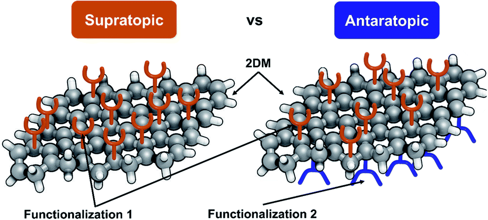 | ||
| Fig. 1 Schematic representation of Janus 2D materials. | ||
Supratopic binding
The one-side functionalization of 2DMs is the most straightforward approach to obtain Janus 2DMs. In this framework, the most extensively used procedure consists of first adsorbing or transferring the 2DM on a solid substrate and then proceeding with the functionalization of its top surface with (macro)molecules via covalent (i.e. chemisorption) or non-covalent (i.e. physisorption) approaches.Janus graphene has been prepared since 2009 by its covalent modification with diazonium salts via the spontaneous electron transfer.8–10 Bekyarova et al. developed the first Janus graphene layer epitaxially grown on a SiC substrate by using 4-nitrophenyl diazonium tetrafluoroborate (4-NBD).8 While the above examples refer to the single chemical modification of Janus graphene, a spatially resolved multicomponent covalent chemical patterning on single-layer graphene on SiO2 substrate has been just recently reported.11 By using a combination of lithography and a self-limiting variant of diazonium chemistry Rodríguez-González et al. demonstrated that up to three different functional groups can be covalently bonded to the basal plane of graphene in a precise, spatially resolved manner.11 Sun et al., reported the functionalization of graphene monolayers grown on copper substrates by chemical vapor deposition (CVD) with 4-NBD.12 The density of grafted molecules could be tuned by varying reaction time and temperature. After the etching of the copper substrate, stacked Janus graphene films can be prepared by using a poly(methyl-methacrylate) (PMMA) graphene bilayer to “fish” one by one other layers of graphene freely floating on water.12 Diazonium chemistry has been applied not only to graphene and related derivatives but also to TMDs. For example, Chen et al. used 4-bromobenzenediazonium tetrafluoroborate to covalently functionalize MoS2.13 The combination of electron beam lithography with surface covalent functionalization enabled the spatial design, engineering, and derivatization of MoS2 nanostructures.13 Covalently bound polystyrene brush layers can be formed on graphene by direct self-initiated photografting and photopolymerization (SIPGP) with styrene which can be excited by free radicals under UV radiation.14,15 The activated monomers initiate a free radical polymerization reaction and create radical sites for surface-initiated polymerization on graphene oxide (GO) by subtracting hydrogen radicals from its surface functional groups such as hydroxyl and epoxy groups.14 Besides, by using electron-beam-induced deposition of carbon, a wide range of vinyl monomers other than styrene could be locally grafted on the surface of graphene.14 On the other hand, Bertolazzi et al. used alkanethiol molecules to covalently functionalized MoS2, by exploiting the notorious capability of thiol functional groups to heal sulfur vacancies in TMDs.16
Casting methods (e.g. drop-casting or spin-coating) have been employed for the non-covalent functionalization of 2DMs.17–24 Strong dopant like tetrafluorotetracyanoquinodimethane (F4-TCNQ) molecules have been physisorbed onto epitaxial graphene (EG) on SiC (0001)17 or monolayer (1L)-MoS2.18 The chemical doping induced by the F4-TCNQ was used to modulate the band structure of EG in the former case whereas it allowed the tuning of the photoluminescence of 1L-MoS2. On the other hand, Hun Yu et al. drop-cast rhodamine 6G (R6G) on 1L-MoS2 to reach an increase of photocurrent by one order of magnitude due to charge transfer of the photoexcited electrons from the R6G molecules to the MoS2 layer.19 Similarly, triphenylphosphine (PPh3) was drop-cast onto WSe2/h-BN devices to improve the photodetector performance due to a doping effect.20 The superatom Co6Se8(PEt3)6 has been used as electron dopant of WSe2 films by Yu et al.21 The fabricated devices have been immersed in the superatom solution which was physisorbed on the WSe2. Alongside, both aliphatic and polyaromatic compounds are known to exhibit a markedly high affinity for the basal plane of various 2D materials, thus they are ideal systems for their non-covalent functionalization. A commercial alkoxy-substituted azobenzene (AZO) molecule (i.e., 4-(decyloxy)azobenzene) comprising a photoresponsive AZO unit grafted at the end of a long alkoxy side chain, was used to form functional adlayer on the surface of 2D semiconductors via their physisorption (i.e. via van der Waals (vdWHs) interactions) promoted by the long alkoxy side chains.22 Supramolecular lattices on graphene can also be bottom-up fabricated by the spin-coating of different molecular building blocks (MBBs) (e.g. 3-trifluoromethyl-3-(3-octadecyloxyphenyl)diazirine) where van der Waals forces drive the interaction between graphene and the self-assembled molecular layer.23 Another most common class of molecules which are known to interact with graphene via strong π–π interactions is pyrene, with its pyrenebutanoic acid succinimidyl ester being thoroughly employed to form ordered hybrids with various 2DMs.24
Janus GO nanosheets functionalized with amino-containing chemicals (e.g. dodecylamine or poly(propylene glycol)bis(2-aminopropylether)) can be prepared via Pickering emulsion template.25 A wax-in-water Pickering emulsion was used to mask one side of GO nanosheets, as GO aggregates on the surface of wax due to the insufficient charge repulsion at lower pH value and strong π–π stacking interaction. Thus, asymmetric chemical functionalization on the aqueous side was performed and Janus sheets were obtained by the removal of the oil phase.25
Microcontact printing (μCP) or macro-initiation assembly of initiator molecules and subsequent surface-initiated atom transfer radical polymerization (SI-ATRP) method has been described as a simple and universal approach to prepare patterned polymer brushes on graphene-based substrate surfaces.26–28 For example, μCP was used to direct the supramolecular assembly of an NH2-terminated pyrene derivative via π–π stacking interactions onto a graphene layer.27 Since the amine is a popular group that is prone to undergo photopolymerization, the resulting photoactive pattern allowed the subsequent grafting of polymer brushes (e.g. polystyrene brushes) via the robust SIPGP.27 Directed self-assembly of block copolymers (e.g. polystyrene-block-PMMA (PS-b-PMMA)) in conjunction with mussel-inspired polydopamine (PDA) universal adhesive enabled the fabrication of device-oriented graphene nanostructures from CVD grown graphene including graphene nanoribbon arrays and a graphene nanomesh.29 Interestingly, the combination of Pickering-type emulsion and grafting-from polymerization via ATRP was used for the asymmetric functionalization of graphene with PMMA.30 A polypyrrole (PPy)–reduced graphene oxide (rGO) Janus-faced film was prepared through a facile and scalable method consisting of the deposition of graphene film on the surface of copper foil via a Cu‖GO electrochemical cell followed by the self-assembly of PPy via interfacial polymerization of pyrrole at the cyclohexane/water (organic/inorganic) interface at low temperature.31
Films of carbon nanotubes (CNTs)32,33 or graphene34 can be prepared at the air/water interface via Langmuir–Blodgett methodology. Janus films were obtained via their asymmetric functionalization by either spray coating of polydimethylsiloxane (PDMS)32,33 or by transferring the films onto a polyethylene surface.34
A compelling strategy for the fabrication of Janus mesoporous silica nanosheets has been proposed by Yan et al.35 Firstly, a mesosilica layer with radially ordered mesopores was coated on PS microspheres via a sol–gel method. Then, surface modification was performed to graft hydrophobic octyl groups on the external surface of the PS@mesosilica microspheres. After the selective removal of PS spheres using tetrahydrofuran, Janus hollow microspheres were obtained. Finally, the hollow microspheres were crushed to present Janus mesosilica nanosheets with perpendicular mesochannels via simple grinding.35 Similarly, MXene nanosheets were grafted on the surface of a positively charged PS template.36 After the etching of the PS microsphere with toluene, the positively charged PS chains were selectively grafted onto one side of the nanosheets, while the other side remained unmodified, leading to the formation of Janus MXene nanosheets.36
Antaratopic binding
Antaratopic Janus 2DMs can be obtained by making use of three main protocols: (i) two-step functionalization assisted by a transfer approach, (ii) functionalization of 2DM surfaces at liquid–liquid or liquid–gas interfaces, and (iii) step-by-step procedure.The first experimental realisation of non-symmetrically modified single-layer graphene was reported by Zhang et al. in 2012 (ref. 37) by employing a two-step surface covalent functionalisation assisted by a poly(methyl methacrylate)-mediated transfer approach. Firstly, a monolayer graphene on silicon oxide/silicon (SiO2/Si) substrate was chlorinated on a single side. Subsequently, a PMMA film was used as a flexible mediator to peel off the single-sided chlorinated graphene from the substrate non-destructively in a 2% HF aqueous solution at room temperature. Finally, phenylation of graphene was performed on the exposed side to fabricate Janus graphene.37 Bissett et al. reported the asymmetric functionalization of CVD monolayer or bilayer graphene by means of diazonium chemistry.38 Firstly, graphene films on PDMS were functionalized on one side with 4-methoxybenzenediazonium tetrafluoroborate (MBD). Subsequently, the opposite side was functionalized with 4-NBD, after the transfer of graphene onto the SiO2 surface.38 A similar protocol was followed by Liu et al. through the one side functionalization of graphene supporter on a copper foil, followed by the Cu etching and transfer mediated by PMMA layer to a SiO2/Si substrate, to accomplish the functionalization of the graphene's opposite side.39 Pyrene derivatives such as 1-pyrenebutyric acid, 1-aminopyrene or 1,5-diaminonaphthalene were utilized for the asymmetric functionalization of graphene.39 Han et al. presented the fabrication of Janus GO/chitosan hybrid membranes via the combination of interfacial self-assembly of GO and chitosan, with subsequent SIPGP from both sides of the GO/chitosan composite membrane.40 Initially, PS brushes were grafted from photoactive sites of the upper surfaces of the composite membrane on silicon wafer through SIPGP. Then, the film was released from the substrate by floating the surface of the substrate with a KOH solution. Finally, poly(2-(dimethylamino)ethyl methacrylate) (PDMAEMA) brushes were grafted on the lower surface of the composite through SIPGP to obtain a distinct Janus structure.40 More recently, Bao et al., reported an approach to synthesize covalently doped graphene superlattices, featuring an asymmetric and spatially defined chemical doping on two opposite sides of graphene (Fig. 2a).41 This approach is based on the combination of two advanced patterned-functionalization principles, namely, laser-writing and PMMA-assisted lithographic processes. A bis(p-chlorobenzoyl)peroxide layer was dip-coated onto a Si/SiO2 wafer prior to the PMMA protected monolayer graphene transfer, allowing for the covalent addition from the bottom-side of graphene via the laser triggered the reaction of bis(p-chlorobenzoyl)peroxide with graphene (Fig. 2a). For the second-step top-side patterned doping, they exposed selected regions and protected the other areas of graphene with a newly covered lithography-defined PMMA layer leading to the first example of patterned Janus graphene (Fig. 2a).41 Differently, GO nanosheets can be electrostatically assembled on PS beads exposing only one GO side for its functionalization.42 Upon dissolving the PS microspheres in tetrahydrofuran (THF) the other side of the GO nanosheets can be subsequently functionalized. By using this approach, Janus GO nanosheets were tailored with hydrophobic PS chains on one side and hydrophilic PDMAEMA chains on the other side.42
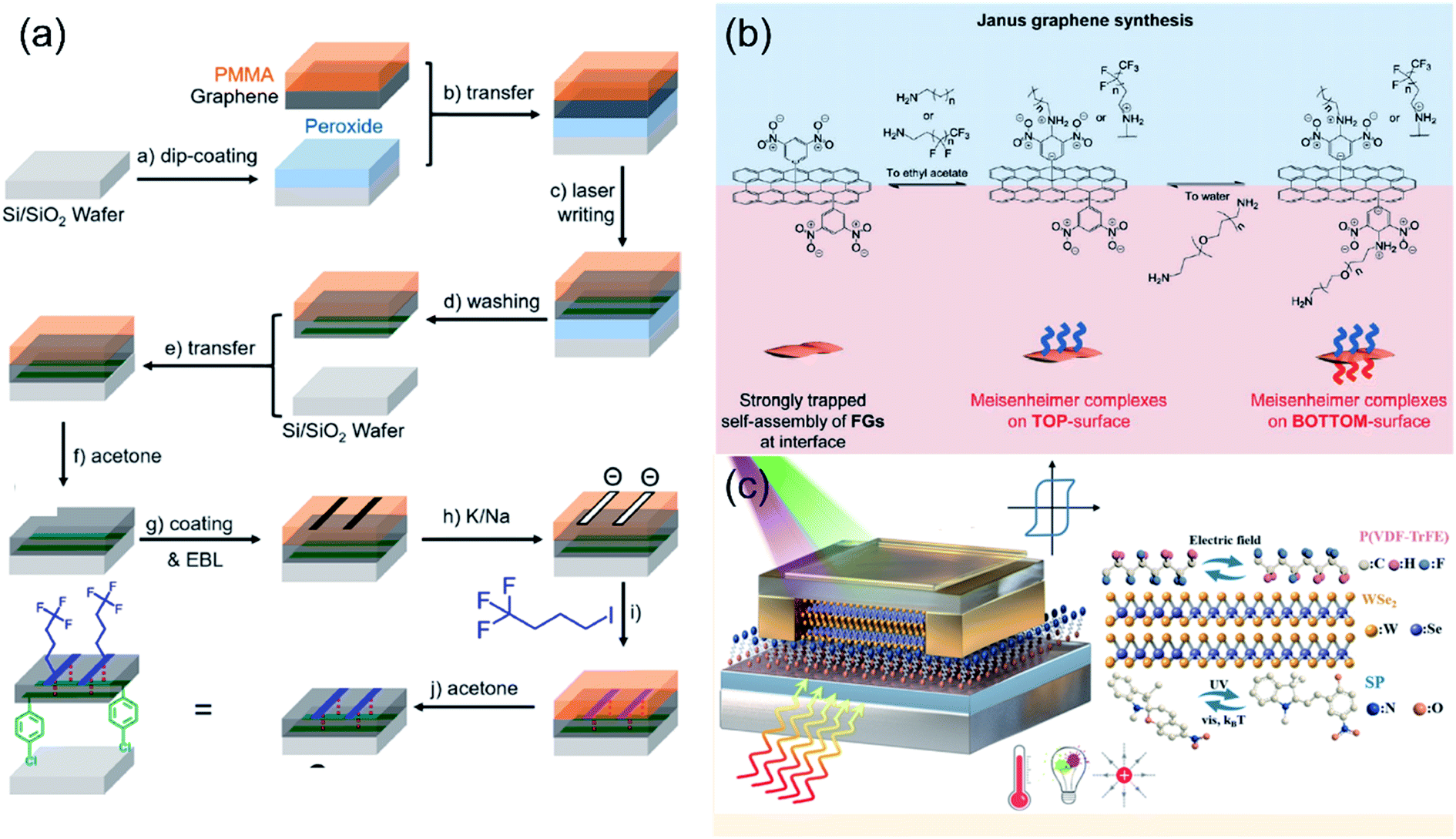 | ||
| Fig. 2 Schematic representation of the three main strategies for the preparation of Janus 2DMs through an antaratopic binding of (macro)molecules. (a) Two-step functionalization assisted by a transfer approach, (b) functionalization of 2DM surfaces at liquid–liquid interfaces and (c) step by step procedure. (a) Adapted with permission from ref. 41, Copyright 2017 American Chemical Society. (b) FGs stands for functionalized graphenes. Adapted from ref. 43 with permission from Wiley-VHC. (c) Adapted with permission from ref. 52, Copyright 2017 American Chemical Society. | ||
The second strategy consists of the use of dynamic covalent chemistry functionalization of 2DMs at liquid–liquid interfaces (Fig. 2b). This approach, introduced by Jeon et al., was exploited for the antaratopic functionalization of graphene (Fig. 2b).43 Graphene was first symmetrically functionalized with 3,5-dinitrophenyl molecules, which allowed its organization at the ethyl acetate–water interface by reducing the intersheet interactions and stacking. The asymmetric functionalization is then accomplished by amine addition to the electron-deficient 3,5-dinitrophenyl groups on the graphene basal planes. The resulting connections involve reversible covalent bonds through Meisenheimer complexes formation, which occurs at liquid–liquid interfaces (Fig. 2b).43 The interface between chloroform and water phase was used for the asymmetric post-functionalization of graphene nanosheets. By employing two different amines (i.e. diethanolamine (DEA) and oleylamine (ODA)), catechol functionalized graphene was obtained with one hydrophobic and one hydrophilic surface being stabilized at the liquid–liquid interface.44 Similarly, the formation of Janus GO monolayers could be achieved by first spreading a solution of amine-terminated PS in toluene on a GO suspension in deionized water; this induced the surface anchoring of the GO at the liquid–gas interface.45 Then, the amphiphilic Janus GO monolayers were obtained by adsorption of the poly(allylamine hydrochloride) (PAH) to another side of the GO monolayer at the interface after injecting the PAH into the aqueous subphase.45 Pickering emulsion strategy can be used for the antaratopic functionalization of 2DMs.46 For instance, Khoee et al. developed a new strategy for the synthesis of Janus GO by the simultaneous anchoring of different polymers with different hydro-affinity. By following this method, alkynyl-modified GO was asymmetrically functionalized with the hydrophobic azidated-poly(3-caprolactone) and the hydrophilic (N-isopropylacrylamide-co-acrylamide-co-allylamine) terpolymer through click reaction.46 More recently asymmetric functionalization of Janus GO nanosheets was achieved in typical oil-in-water Pickering emulsion by combining ATRP (i.e. with poly(2-(acryloyloxy)ethyl ferrocenecarboxylate) (PMAEFc)) and mussel-inspired chemistry (i.e. with PDA).47 Differently, Jang et al. reported a one-step process to realize Janus-structured nanocomposites with iron oxide (Fe3O4) nanoparticles (Fe3O4 NPs) and PDA on each side of a GO nanosheet using the Langmuir–Schaefer technique.48 Han et al. reported the fabrication of Janus nanosheets with lamellar structures at the air/liquid interface of a water-miscible organic solution of fatty acids and an aqueous solution of metal ions.49 The formation of the nanosheets was the result of self-assembly of fatty acid molecules and metal ions due to the hydrophobic interaction between the alkyl chains, and the coordination between the carboxylic groups and the metal ions, which was induced by the spreading of the organic solution at the interface and the mutual diffusion between the organic solution and the aqueous solution.49 On the other hand, Janus silica nanosheets were prepared by a self-assembled sol–gel process at the emulsion interface by combining a Pickering-type emulsion.50 In essence, Janus silica nanosheets with a hydrophobic surface (capped with 3-chloropropyl groups) and a hydrophilic surface (capped with amino-groups) were fabricated by crushing Janus composite hollow spheres resulting from the self-organized sol–gel process at amphiphilic emulsion interface.50
The last approach consists of a step-by-step protocol (Fig. 2c). This method was first introduced by Stoeckel et al. by accomplishing an asymmetric double-side functionalization of a bilayer WSe2 with two different molecules.51 A chemisorbed self-assembled monolayer (SAM) of [3-(trimethoxysilyl)propyl]ethylenediamine (AHAPS), which determines an n-type doping, was first created on a SiO2 substrate. Then, a mechanically exfoliated WSe2 bilayer was transferred onto SAM-functionalized SiO2 substrates. Subsequently, the same bilayer was treated with trichloro(1H,1H,2H,2H-perfluorooctyl)silane (PFS) vapor to induce p-type doping in the top layer. This approach was later extended by Qiu et al. for the asymmetric functionalization of a bilayer WSe2 (ref. 52) (Fig. 2c) or few layers thick WSe2 (ref. 53) with light-responsive molecules (i.e. spiropyran52 or diarylethene53) and ferroelectric polymer (i.e. poly(vinylidene fluoride-trifluoroethylene) (P(VDF-TrFE))52,53) to realize field-effect transistors (FETs) based multiresponsive multilevel non-volatile memories (Fig. 2c).
3. Properties tailoring and (multi)functionality
The asymmetric functionalization of 2DMs with (macro)molecules can lead to mainly two effects: (i) tailoring of the surface properties, and (ii) chemical doping. The former is the clear case of a Janus material, as involves materials where each side possesses distinct surface properties, such as wettability and chemical reactivity. The latter involves the properties that are enhanced or generated due to the chemical doping with (macro)molecules, such as electronic properties, photoresponse or photoluminescence. Although chemical doping is not restricted to Janus materials, the exposure of the two faces of the 2DMs to different local environments may lead to novel routes for band gap tuning and it also paves the way for the development of multi-responsive materials.Wettability
By using an analogous approach as in the lotus leaf, Janus 2DMs exhibiting bifacially anisotropic wettability can be obtained.25,27,28,30,36,37,40,42,45,49,54 Zhang et al., reported the fabrication of Janus graphene through the co-grafting of halogen and aryl/oxygen-functional groups on each side.37 Interestingly, they demonstrated that the chemical functionalities on one side are capable of affecting both chemical reactivity and surface wettability of the opposite side, indicating the existence of a cross-talk between the two groups grafted on the two sides of the carbon interlayer. Single-sided chlorination results in a decrease in the water contact angle (CA) of graphene, from 84.7° to 32.6°, owing to the formation of C–Cl bonds, which would increase surface energy and simultaneously introduce polarity. The CA of the opposite side, however, slightly dropped to 69.9°, indicating that the chlorine groups are capable of influencing the wettability of the opposite side. Then, phenylation results in reduced wettability of the exposed surface and the CA increased to 89.9° after introducing the phenyl groups. At the same time, the CA of the chlorinated side was found to also increase from 32.6° to 59.6°. The influence of the one-side functionalization over the opposite side originates from the extreme thinness of the medium single carbon layer and the polarity introduced by the formation of covalent bonds.37Among the great number of examples of amphiphilic Janus 2DMs, Janus silica nanosheets asymmetrically decorated with poly(2-(acryloyloxy)ethyl ferrocenecarboxylate) and polydopamine exhibit an incredibly high anisotropic surface wettability.54 The contact angle of the hydrophobic surface of the SiO2@PMAEFc/PDA Janus nanosheets was 138.6° which reveals that the SiO2@PMAEFc/PDA Janus nanosheets possess hydrophobic properties after grafting PMAEFc. The contact angle of the hydrophilic surface amounted to 35.1° indicating that the surface of the Janus nanosheets modified with PDA possesses excellent hydrophilicity. The difference of CA reaches as high as ∼103.5° which demonstrates dramatic disparity on surface properties of two sides.54
Chemical reactivity
Bissett et al. performed the asymmetric functionalization of CVD monolayer or bilayer graphene with a p-type (i.e. 4-NBD) and an n-type (i.e. MBD) molecules.38 Interestingly, the net doping of the Janus graphene was found to be p-type, revealing that the number of NBD molecules covalently bonded to the graphene was larger than the number of MBDs, thus indicating that functionalization of one side of the graphene plane could lead to an increase in the reactivity of the opposite side.38Gao et al. employed polymer brushes with different functionalities including cationic and anionic polyelectrolyte, thermally and pH-responsive polymers, as well as polymer patterns on different graphene-based surfaces to demonstrate the broad applicability of their fabrication strategy, based on the microcontact printing of initiator molecules and subsequent surface-initiated atom transfer radical polymerization method.26
One of the most common applications of amphiphilic Janus nanomaterials is the stabilization of the oil–water interface by lowering the interfacial tension.30 For instance, the PMMA-functionalized face prefers an orientation toward the chloroform phase, while the non-modified (i.e., GO) face of the Janus nanosheet prefers being exposed to water, in a similar vein to an assembly of these nanosheets at the air–water interface in LB films. Although symmetric systems (e.g. GO decorated with PMMA) are able to decrease the interfacial tension of chloroform/water system, the magnitude of such an effect is greater when asymmetric materials are used.30
Electronic structure and charge transport properties
Band gap tuning or band gap engineering are instrumental for the production of materials with different electronic and optical properties.55 Among others, chemical doping is a viable approach for opening a band gap in graphene and modifying its Fermi level, thereby modulating the 2DMs-based device's characteristics.56 Chemical doping involves either a (1) charge transfer process between 2DMs and (macro)molecules or (2) molecular-dipole-induced shift in the 2DM work function.57–60 In the case of a charge transfer process, a difference in electronic chemical potentials at an interface is required, which is determined by the relative positions of the 2DM Fermi level and the highest occupied (HOMO) and lowest unoccupied (LUMO) molecular orbitals of the (macro)molecules. In contrast, dipole-mediated doping can potentially take place any time that polar (macro)molecules are interacting with the surface of 2DMs.The band structure and hence the electronic properties of epitaxial graphene can be precisely tailored via the covalent functionalization of the graphene surface via diazonium chemistry.8,10 The chemical formation of carbon–carbon bonds comprises the re-hybridization of the carbon centers from sp2 to sp3, which introduces a barrier to electron flow by opening a band gap thereby yielding the generation of insulating and semiconducting regions in graphene wafers.8 For instance, 4-nitrophenyl diazonium tetrafluoroborate allowed the tuning of the electronic structure and transport properties of the EG from near-metallic to semiconducting.8 In an analogous manner, the conductivity of monolayer graphene nanoribbons (GNRs) gradually decreased with the diazonium (4-NBD) treatment time.9 However, graphene devices treated with a 4-bromobenzene diazonium salt did not show any altered conductance at the neutrality point, which highlights the importance of the chemical structure of the (macro)molecules to modulate the doping effects.10
The band structure of epitaxial graphene can also be precisely tailored through the functionalization of the graphene surface with a strong electron acceptor like F4-TCNQ.17 A charge-transfer complex is formed between the graphene film and the F4-TCNQ molecules, where the electrons are removed from the graphene layer via the cyano groups of the molecule, allowing to achieve charge neutrality in monolayer and bilayer graphene.17 In bilayer graphene, the hole doping even allowed the Fermi level to shift into the energy bandgap, and the additional dipole developed at the interface with the F4-TCNQ layer determined an increase of the band gap size to over twice its original value. Thus, the electronic structure of the graphene bilayer can be precisely tuned by varying the molecular coverage.17
Photoresponse
The 2DMs photoresponse can be modulated through a charge transfer process occurring between 2DMs and suitably designed (macro)molecules. MoS2 is notorious to suffer from a major disadvantage for optoelectronic applications, i.e. its persistent photoconductivity (PPC).61 Hence, the suppression of this PPC effect is key to exploit the light–matter interaction in MoS2 hybrids for technological applications. We have recently developed mixed-dimensional van der Waals heterostructures based on a large macromolecule, i.e. graphene nanoribbons (GNRs) with an armchair-type edge structure and seven carbon atoms in width (7-AGNR), physisorbed onto 2D MoS2 and demonstrated that such interfacing enables to efficiently suppress the PPC effect of MoS2 as a result of interfacial charge transfer process. The latter is evidenced by a threefold reduction of the hysteresis width, and more stable transfer characteristics upon switching between light irradiation and dark conditions. This platform is thus most suitable to phototune the charge transport in MoS2–GNR based field-effect transistors when further functionalized with photochromic molecules.62Another proof-of-concept was achieved by simply drop-casting a commercially available R6G organic dye (optical band gap = 2.38 eV, λmax = 521 nm) onto the MoS2 surface. Such interfacing is accompanied by a dramatical enhancement of the electrical response of the device to light irradiation over the range 681 nm < λ < 980 nm, which is the forbidden optical absorption region for pristine MoS2 photodetectors.19
Similarly, a TMD-based photodetector was fabricated by drop-casting triphenylphosphine on WSe2/h-BN devices.20 After the PPh3 deposition, the Fermi level of WSe2 moved toward the conduction band edge (n-type doping phenomenon). The n-doping originated from the electron transfer phenomenon from the lone pair of phosphorus atoms in PPh3 which resulted in both a fast temporal photoresponse and a high responsivity of the WSe2/h-BN devices.20
Photoluminescence (PL)
Chemical doping allows not only to tune of the electrical properties of 2DMs but also their optical properties. For example, the PL intensity of 1L-MoS2 can be drastically enhanced by the adsorption of p-type dopants (e.g. F4-TCNQ and TCNQ) with high electron affinity but reduced through the adsorption of n-type dopants (e.g. nicotinamide adenine dinucleotide (NADH)).18 The PL enhancement when p-type dopants cover the 1L-MoS2 surface is understood as a consequence of switching the dominant PL process from the recombination of the negative trion to the recombination of the exciton under extraction of residual electrons in as-prepared 1L-MoS2. In contrast, the PL intensity is reduced when 1L-MoS2 is covered with n-type dopants, which is due to the suppression of exciton PL by the injection of excess electrons.184. Applications
Energy storage: batteries and supercapacitors
In a seminal work, Sun et al. reported an artificial graphite nanostructure as anode for Na+ storage, which consists of stacked graphene sheets, with the upper face of each sheet being functionalized with 4-nitrobenzene diazonium tetrafluoroborate.12 After grafting, the nitrobenzene functional group was easily converted into an aminobenzene (AB) by electrochemical reduction, with the latter moiety acting both as graphene spacer and as an active site for Na+ (Fig. 3a). Each AB moiety in-between two stacked graphene sheets is connected by a covalent bond to the lower graphene sheet and it interacts via electrostatic interactions with the upper graphene sheet, resulting in a unique structure. The surface properties of graphene abruptly changed upon the introduction of the AB functional group (e.g. hydrophilicity), while the geometry of the opposite surface was preserved. This controllable surface change allowed the preparation of stacked Janus graphene layers with much better alignment versus pristine graphene, due to the weak interlayer interaction. More importantly, this Janus graphene can be intercalated/deintercalated with Na+ ions in a reversible and stable way, in contrast to graphite or stacked graphene, which makes it a promising material for sodium-ion batteries (SIBs) (Fig. 3b and c).12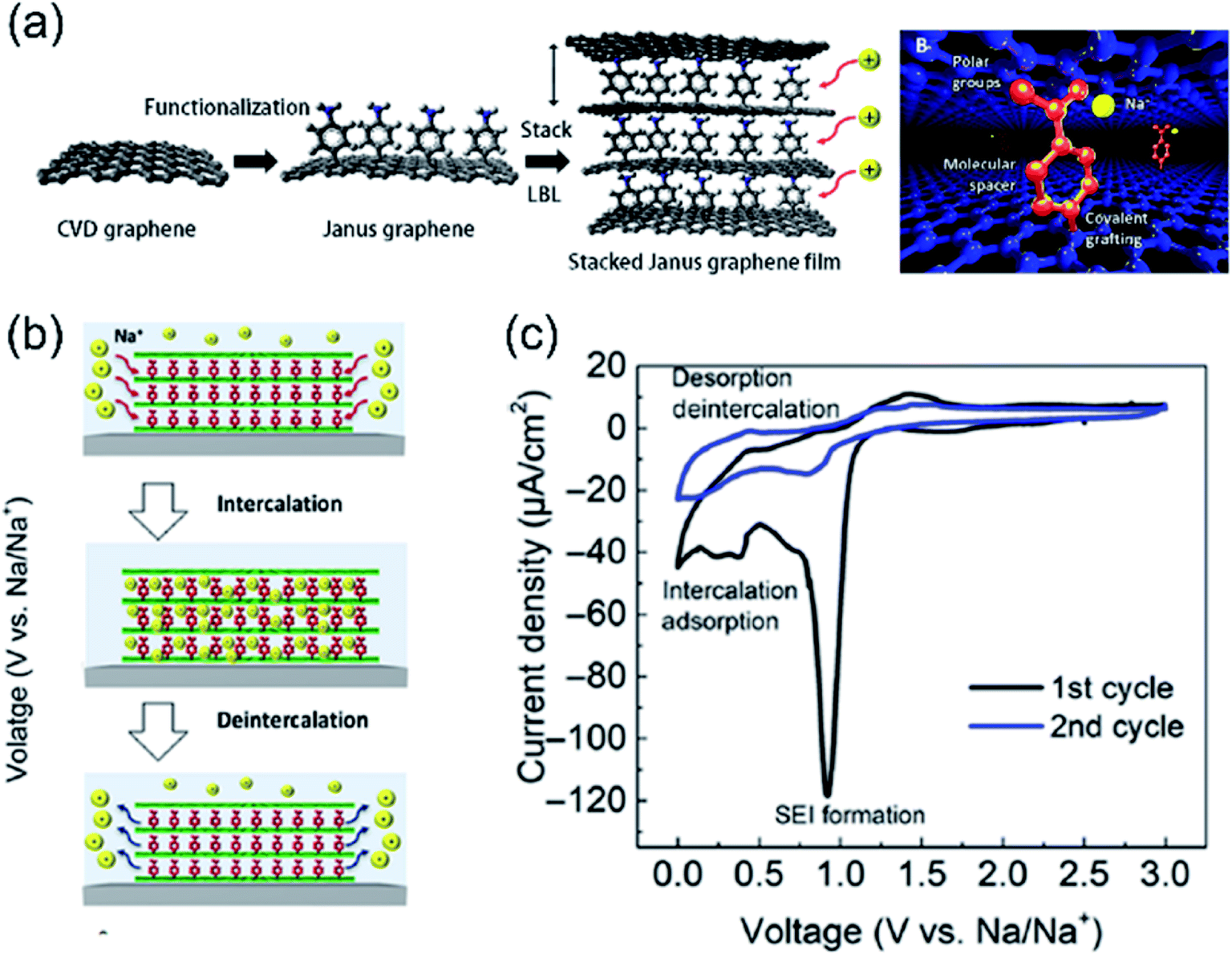 | ||
| Fig. 3 (a) Schematic illustration of the preparation of the Janus graphene and the stacked Janus graphene thin film, LbL stands for Layer-by-Layer, (b) scheme of the different intercalation/deintercalation cycle of Na+ in AB graphene, and (c) CV curves measured during the first two cycles of Na+ intercalation in AB graphene. The sweep rate was 0.042 mV s−1. The first curve shows a sharp cathodic peak, which disappears in the second cycle, corresponding to the formation of a stable solid electrolyte interphase (SEI). Adapted from ref. 12 with permission of Science. | ||
Zhang et al. proposed a facile approach to construct a Janus-faced film electrode with dual-conductive/pseudo-capacitance function for flexible supercapacitor by taking advantage of the high electric conductive of graphene and high pseudocapacitive performance of polypyrrole and together with the strong π–π coupling effect between graphene and polymer nanosheets.31 The resulting electrode exhibited ultra-high specific capacitances (1380 mF cm−2 at 1 mA cm−2) and excellent rate capability (65.1% capacitance retention with the current density increases to 20 mA cm−2). Furthermore, the assembled PPy–rGO//PPy–rGO symmetric supercapacitors delivered a maximum energy density of 31.95 W h L−1, remarkable cyclic stability (89.7% capacitance retention after 10![[thin space (1/6-em)]](https://www.rsc.org/images/entities/char_2009.gif) 000 cycles) and superior mechanical property (82% capacitance retention after 8000 cycles under different bending conditions).31
000 cycles) and superior mechanical property (82% capacitance retention after 8000 cycles under different bending conditions).31
Jang et al. reported a Janus-structured thin film with carbon-based GO, Fe3O4 NPs, and PDA to achieve a high-capacity and long-life anode material.48 The Fe3O4 NPs were chosen due to their high capacity, but their main drawback is that they suffer from low conductivity and large volume expansion, which causes structural defects, thus decreasing the battery life. However, their synergistic combination with GO, which improved electrical conductivity and mechanical stability, allowed the GO hybrid to be used as a high-capacity active material. On the other hand, PDA is added as a binder due to its unique wet-resistant adhesive property. This Janus multilayer electrode exhibited an excellent capacity of ∼903 mA h g−1 at a current density of 200 mA g−1 and a reversible capacity of ∼639 mA h g−1 at 1 A g−1 up to the 1800th cycle, indicating that this Janus composite can be a promising anode for Li-ion batteries.48
Field-effect transistors (FETs)
WSe2 holds great potential as an active component for logic circuitry as it is a layered ambipolar semiconductor enabling transport of both hole and electron. However, solid-state devices based on single- and bilayer WSe2 typically exhibit unipolar transport and poor electrical performance when conventional SiO2 dielectric and Au electrodes are used. To tackle this problem, Stoeckel et al. performed a single or double-side asymmetric functionalization of a mono- or bilayer WSe2 respectively with silane-containing molecules.51 They demonstrated an alternative strategy by engineering the WSe2 energy levels to match the Au Fermi level. In this way, the molecularly engineered WSe2 single layers FET, contacted with conventional Au contacts on SiO2 dielectrics show p- or n-mobility as high as μh = 150 cm2 V−1 s−1 and μe = 17.9 cm2 V−1 s−1. Alongside, they showed opposite polarity to the top and bottom layer of bilayer WSe2, demonstrating nearly balanced ambipolarity at the bilayer limit. The combination of energy level engineering and defect functionalization offers the possibility of providing the desired charge transport characteristics to atomically thin WSe2 and, hence, demonstrate high-performance field-effect devices.51Hybrids composed of 2D transition metal dichalcogenides with stimuli-responsive molecules are prototypical components for the development of multifunctional FETs, whose output currents can be remotely controlled by external inputs. For instance, Zhao et al. showed that monolayer MoS2 decorated with ferrocene-substituted alkanethiol (Fc-SH) molecules not only improved the FET performance but also showed reversible electrochemical switching on the surface of MoS2.63 The thiol group in Fc-SH molecules can improve the FET performance by healing the sulfur vacancies of monolayer MoS2, while the ferrocene group in the molecules is responsible for the tunable doping on 2D semiconductor via reversible switching between neutral and positively charged states. The field-effect mobility of monolayer MoS2 reached values as high as ≈116 cm2 V−1 s−1 with Ion/Ioff ratio exceeding 105. The authors demonstrated for the first time the tunable molecular doping effect on the electrical transport of 2D semiconductors via electrochemical stimuli.63
The functionalization of 2DMs with light-responsive molecules like azobenzene22 or 3-trifluoromethyl-3-(3-octadecyloxyphenyl)diazirine23 can offer an efficient protocol for the development of high-performance multifunctional materials and devices. For instance, Zhao et al. reported an universal approach to optically switch 2D electronics by fabricating hybrid vdWHs comprising 2D semiconductors (i.e. MoS2 or BP) coated with a photochromic AZO adlayer, supported on a trap-free polymer dielectric.22 The joint effect of the improved 2D/dielectric interface, the molecule's light-modulated dipolar doping, and the high thermal stability of cis-AZO offered the highest control over the reversible and efficient charge carrier tuning in 2D semiconductors with a preserved high performance in 2D field-effect transistors, as quantified in terms of carrier mobility and Ion/Ioff ratio. The device has the potential to operate as an optical memory with four current levels and a long retention time (>15 h).22 Gobbi et al. showed that hybrid vdW heterostructure composed of a 2D supramolecular lattice (SL) self-assembled on graphene, represents an ideal system for generating periodic potentials whose periodicity, amplitude and sign can be pre-programmed by careful molecular design.23 The amplitude of the periodic potential is mediated by the specific interaction between graphene and molecular dipoles, while the nanoscale periodicity is determined by the geometry of the self-assembly. In particular, by using a photoreactive organic molecule, a subtle photo-induced change in the chemical structure of the starting molecule leads to a different amplitude of the potential, while leaving the periodicity unaltered.23 As a step further, Qiu et al. reported the fabrication of ternary-responsive FETs based on a few-layer WSe2 by decorating the two opposite surfaces of the 2D semiconductor with different stimuli-responsive molecules in an asymmetric fashion.53 The bottom side is dressed with a photochromic diarylethene (DAE) film and the top side with a ferroelectric P(VDF-TrFE) layer (Fig. 4a and b). The synergy between the two molecularly induced effects enabled the devices to respond orthogonally to an electric field and light irradiation, with an enhanced output current modulation efficiency of 87%. The 9 ferroelectric and 84 photo-generated states ensure 756 current levels in a single device. In addition, the devices demonstrated excellent performance in cyclic endurance (10 cycles) and data retention (over 1000 h), paving the way for their application as high-density non-volatile memories (Fig. 4c–h).53
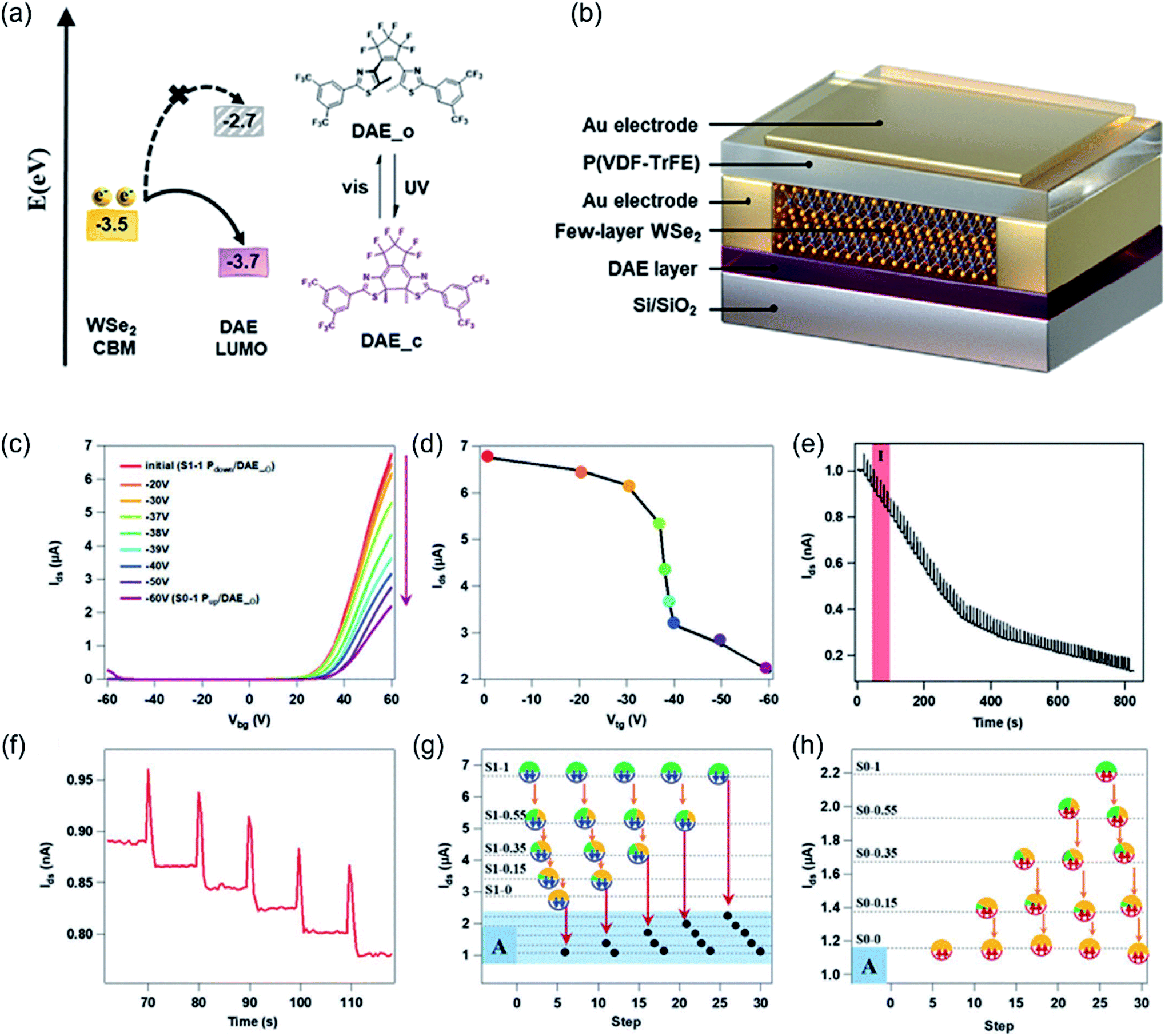 | ||
| Fig. 4 (a, b) Energy level diagram between DAE and WSe2, device geometry, and electrical characterization of P(VDF-TrFE) capacitor and DAE/WSe2/FeFET. (a) Energy level diagram of the electron transport between DAE/WSe2 and the chemical structures of investigated DAE molecules, (b) schematic diagram of the DAE/WSe2/FeFET device with double-sided decoration: the bottom surface with DAE film and the top surface with P(VDF-TrFE) layer. (c–h) Multilevel storage of DAE/WSe2/FeFET. (c) Transfer evolution when partially polarizing the P(VDF-TrFE) from downward to upward direction by the sweeping top gate at various ranges. (d) Corresponding Ids current evolution behavior at Vbg = 60 V as a function of a programmed sweep. (e, f) Dynamic Ids current evolution behavior under exposure of short UV pulses at Vbg = 0 V: (e) totally obtained 84 levels and (f) enlarged 5 levels in region I. (g) Multilevel current over five cycles by different stimuli orders. (h) Enlarged levels in region A. Adapted from ref. 53 with permission from Wiley-VHC. | ||
In another recent example of Qiu et al., a quaternary-responsive WSe2-based FET whose output current can be remotely and reversibly controlled by light, heat, and electric field was fabricated.52 A photochromic silane-terminated spiropyran (SP) is chemisorbed on SiO2 forming a SAM that can switch from the SP to the merocyanine (MC) form in response to UV illumination and switch back by either heat or visible illumination. Upon UV irradiation, a drastic decrease in the output current of 82% can be observed and ascribed to the zwitterionic MC isomer acting as a charge scattering site. To provide additional functionality, the WSe2 top surface was coated with a ferroelectric co-polymer layer based on P(VDF-TrFE). Because of its switchable inherent electrical polarization, it can promote either the accumulation or depletion of charge carriers in the WSe2 channel, thereby inducing a current modulation with 99% efficiency. The synergistic effect between the different stimuli enabled a significant modulation of the charge carrier transport within the channel switching from n-type to p-type with electrons being fully depleted. Such control over the carrier concentration and device polarity is key to develop 2D advanced electronics.52
Photodetectors
A single-layer MoS2 treated with light-sensitive rhodamine 6G organic dye molecules was used as photodetector, exhibiting an enhanced performance with a broad spectral photoresponse and a high photoresponsivity compared with the properties of the pristine MoS2 photodetectors.19 The R6G dye molecules deposited onto the MoS2 layer increased the photocurrent by an order of magnitude due to charge transfer of the photoexcited electrons from the R6G molecules to the MoS2 layer. The resulting device exhibited a maximum photoresponsivity of 1.17 A W−1, a photodetectivity of 1.5 × 10⁷ jones, and a total effective quantum efficiency (EQE) of 280% at 520 nm.19On the other hand, Jo et al. fabricated a photodetector with high responsivity and fast switching speed through the sequential deposition over a SiO2 substrate of: (i) a h-BN layer, (ii) a WSe2 layer and (iii) a PPh3 layer acting as an n-doping species (Fig. 5a).20 The authors demonstrated that by applying the h-BN layer at the WSe2/SiO2 interface the maximum photoresponsivity was 1.27 × 10⁶ A W−1 under 5 pW laser exposure, and the rising and decaying times were 2.8 ms and 20.8 ms, respectively, which are comparable to or better than the performance of the Pt-contacted WSe2 photodetector (Fig. 5b–e).20
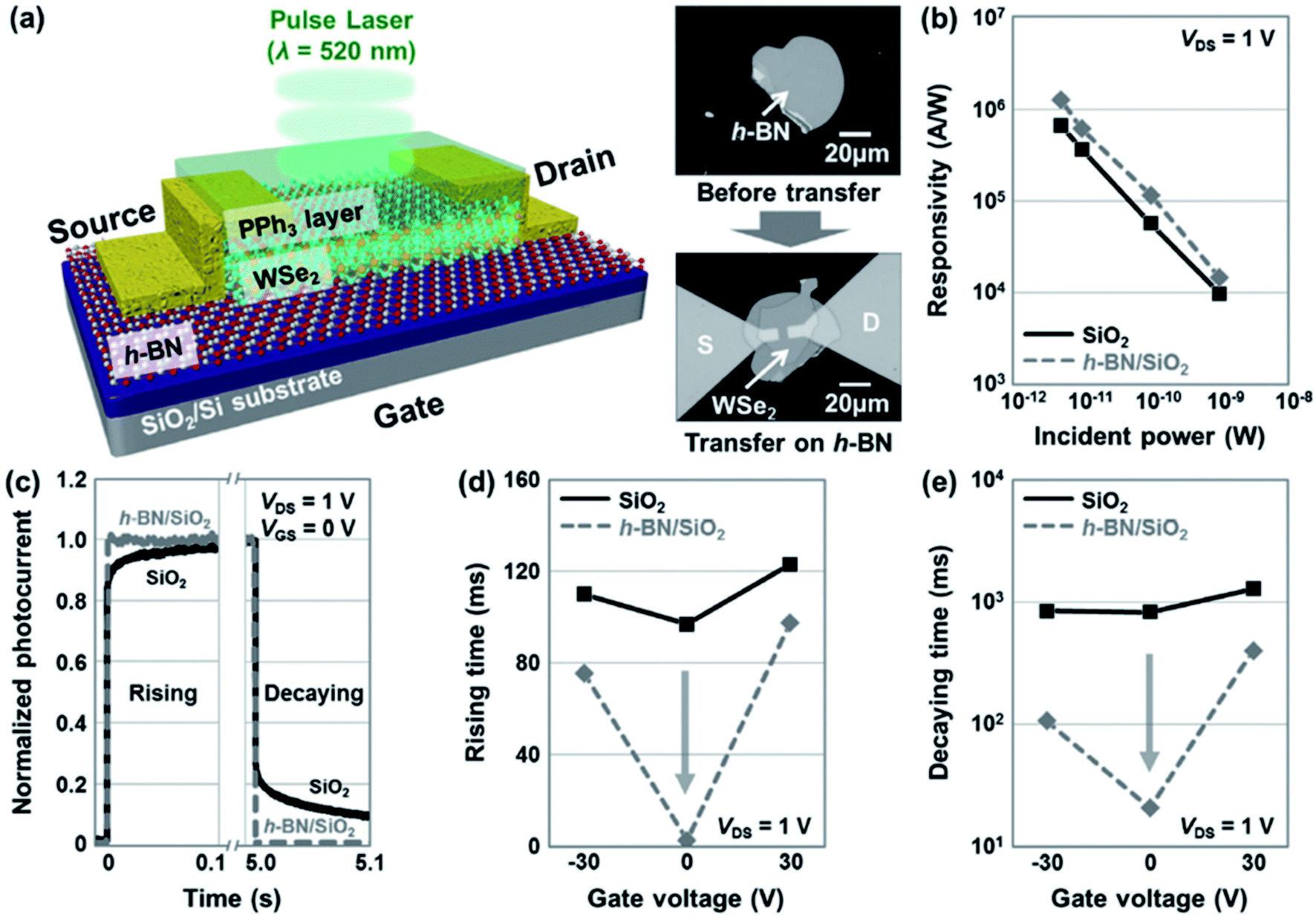 | ||
| Fig. 5 Characterization of PPh3-doped Ti–WSe2/h-BN photodetectors. (a) Schematic diagram and optical images (before and after transfer) of h-BN inserted into the Ti-contacted WSe2 photodetector that was doped by 7.5 wt% PPh3. (b) Extracted photoresponsivity as a function of the incident laser power (5, 10, 100, and 1000 pW) before and after transferring to the h-BN/SiO2 substrate. (c) Normalized temporal photoresponse curves at the rising and decaying edges. (d, e) Rising (d) and decaying (e) times of the photodetector as a function of the gate voltage (VG = −30, 0, and 30 V), where the drain voltage (VDS) was 1 V. Adapted from ref. 20 with permission from Wiley-VHC. | ||
Photovoltaic devices
Graphene is a very promising material for replacing indium tin oxide (ITO) as an anode in organic photovoltaic devices due to its inherent low-cost fabrication process and outstanding conductivity and optical transparency. However, graphene films feature a poor hydrophilicity, leading to a negative effect on the construction of solution-processed devices. This problem was overcome by Wang et al. where they modified the surface of graphene with pyrene butanoic acid succinimidyl ester using the non-covalent chemical functionalization method.24 This allowed an improvement of the power conversion efficiency (PCE) to 1.71%. This performance corresponds to ∼55.2% of the PCE of a control device based on ITO/poly(3,4-ethylenedioxythiophene):poly(styrenesulfonate)/poly(3-hexyl)thiophene:phenyl-C61-butyric acid methyl ester/LiF/Al electrodes (PCE = 3.1%).24Catalysis
Yan et al. reported a novel Janus mesosilica nanosheet with perpendicular mesochannels prepared by simply crushing hollow microspheres.35 These nanosheets were used as interface-active particles to immobilize metal nanoparticles for enhanced biphasic catalysis. The hydrophobic octyl groups were selectively modified on one surface of the mesosilica nanosheets and ultrafine Pd nanoparticles were uniformly loaded in the mesochannels. Fig. 6d shows a high-angle annular dark-field imaging-scanning transmission electron microscopy (HAADF-STEM) image of Janus catalyst Pd/mSiO2 nanosheet. These nanosheets not only displayed an excellent interfacial activity but also provided a highly accessible reaction interface for oil- and water-soluble reactants. As displayed in Fig. 6a, the nitrobenzene reduction was completed in only 30 minutes by using the Janus system whereas other catalysts are much slower or not able to reach a 100% of conversion. Such a Janus nanosheet-based catalyst showed a significantly enhanced activity in aqueous nitroarene hydrogenation reactions, 13-fold and 4.6-fold higher than those of the hydrophilic counterpart and conventional silica-based interfacial catalyst, respectively (Fig. 6b).35 Another important factor for a catalyst is their reusability, as can be seen in Fig. 6c, after 5 cycles the performance of the Janus system was barely affected.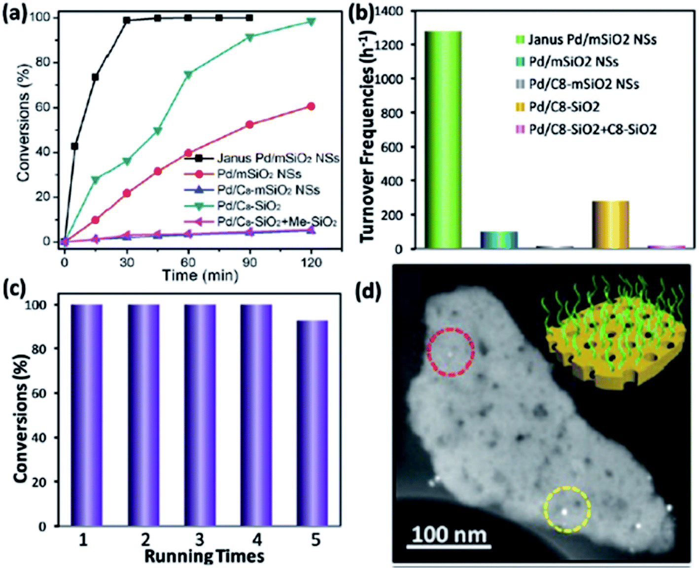 | ||
| Fig. 6 (a) The kinetic profile for nitrobenzene reductions over different catalysts under stirring-free conditions. (b) Comparison of turnover frequencies (TOFs) for different catalysts. (c) Recyclability test of Janus Pd/mSiO2 nanosheet in biphasic hydrogenation, reaction time: 1.5 h. (d) High-angle annular dark-field imaging-scanning transmission electron microscopy (HAADF-STEM) images of Janus catalyst Pd/mSiO2 nanosheet. Adapted from ref. 35 with permission from The Royal Society of Chemistry. | ||
Drug delivery
Khoee et al. demonstrated that an amphiphilic Janus graphene can be used as an effective platform for the simultaneous delivery of two hydrophobic and hydrophilic drugs by means of one carrier which has the ability to be loaded with both drugs in order to treat the cancerous cells synergistically.46 A thermo-responsive NIPAAm-based nanocarrier system was developed as hydrophilic domain to be loaded with 5-FU and biocompatible PCL as hydrophobic one to be loaded with quercetin. The authors studied the drug release and toxicity tests at two different temperatures and they concluded the Janus graphene system showed low toxicity and the highest drug release was achieved at 40 °C.46Georgitsopoulou et al. reported that their amphiphilic Janus graphene was dispersible in both chloroform and water, in which it formed different superstructures.44 The multilayered superstructures that were formed in water have a hydrophobic internal space which is capable to host organic molecules and hence could be used as a substrate in drug-delivery systems.44
Self-healing materials
Chemically asymmetric Janus 2DMs have outstanding application prospects for the development of smart materials.47,54 Hydrogels have received increased attention due to their promising applications in wound dressing, tissue engineering, biosensors and human–machine interfaces. Ma et al. reported that the antaratopic Janus GO, where poly(2-(acryloyloxy)ethyl ferrocenecarboxylate) and polydopamine were grafted on the two opposite sides of GO, was successfully applied as self-healing nanocomposite hydrogels.47 Subsequently, self-healing hydrogels were successfully prepared by incorporating Janus GO–PMAEFc/PDA and FeCl3·6H2O into the poly(acryloyl-β-cyclodextrin) (PACD) associated polyacrylic acid (PAA) hydrogels. The joint effect of metal–ligand coordination bonds (i.e. Fe(III)–catechol groups) and host–guest bonds (i.e. ferrocene–β-cyclodextrin) imparts to the dual self-healing hydrogels excellent self-healing properties (self-healing efficiency can reach 93.4% within 1 h) and mechanical strength (tensile strength of 0.94 MPa and strain of 508.5%).47Analogously, silica nanosheets modified with PMAEFc and PDA were used as robust reinforcement to design self-healing nanocomposite hydrogels.54 Based on multiple effects of metal-coordination and host–guest interactions, the mechanical strengths and self-healing properties of hydrogels were both enhanced. In particular, after introducing Janus nanosheets, the rupture stress of hydrogels increased from 1.27 MPa to 2.23 MPa, and the self-healing efficiency improved from 66.7% to 92.4%.54
Sensors
Although several Janus 2DMs hold great potential to be used as sensors or actuators, to the best of our knowledge their practical use has been only slightly pursued.11,37,41,63 For example, the spatially resolved multicomponent covalent chemical patterning of single-layer graphene offers exciting opportunities for applications in electronics, catalysis, sensing, or photonics.11 Such ultrathin, well-defined layers of covalently bound functional groups are extremely promising for sensing applications, where dense yet non-passivating films are desired for ensuring efficient electron transfer across the interface.11 Differently, the MoS2-based FET decorated with ferrocene-substituted alkanethiol has huge technological potential for the development of electrochemically switchable 2D devices and provides an enlightening guidance on electrochemical sensing devices.63 Gao et al. fabricated DNA arrays on PET for sensor and diagnostic applications by using graphene supratopically decorated with poly glycidyl methacrylate (PGMA@G).28 PGMA is well known to react with amines and has been used to immobilize biomolecules, such as DNAs, proteins and enzymes. Hence, PGMA@G on PET was used to immobilize an oligonucleotide which allowed for the selective DNA sensing via a fluorescence assay.28Selective capture and separation of small molecules
Molecularly imprinted polymers (MIPs), often named as synthetic antibody mimics, are capable of specific molecular recognition for a target molecule. On the other hand, magnetic NPs can be easily collected and separated by an external magnetic field without additional centrifugation or filtration. Wang et al. integrated into a single platform a recognition element (i.e. MIP) and fast separation element (i.e. Fe3O4 NPs) of 2′-deoxyadenosine (dA).50 By combining the two-sidedness of Janus silica nanosheets, surface imprinting technique and magnetic molecularly imprinted composites integrated Janus-like magnetic molecularly imprinted polymers were synthesized for specific separation and fast separation of a small molecule such as dA where the equilibrium time was 70 min, and the maximum monolayer adsorption was calculated to be 61.22 μmol g−1 at 25 °C.505. Conclusions and future outlook
We have reviewed the state-of-the-art of Janus 2DMs prepared by their asymmetric functionalization or through the exposure of their two faces to different local environments. We showcased the most recent strategies for the preparation of Janus 2DMs by supratopic or antaratopic binding with (macro)molecules. The unique properties of 2DMs asymmetrically decorated with (macro)molecules can be utilized to enhance and enrich the surface functionality, and the electronic and optical performance of the much less reactive pristine 2DMs. The major applications of Janus 2DMs fall into two areas: (i) electronic applications and (ii) stimuli-driven actuators. However, some relevant examples in energy storage and generation, catalysis, drug delivery, smart materials, sensors and selective capture and separation applications have also been recently reported.It is important to point out that this research field is still in its infancy and most of the research to date has been focused on the fundamental preparation and understanding of these novel materials.64 The examples described in this perspective comprised graphene, graphene family, TMDs, MXenes, nanosheets with lamellar structures and silica nanosheets. In fact, other 2DMs such as metal oxides, nitrides, carbides or BP have not been yet explored in the recently growing field of Janus 2DMs. To realize real-world applications, more efficient and low-cost Janus 2DMs fabrication strategies should be developed in the future. Among the fabrication procedures reported, the step-by-step procedure, that we have proposed opens the possibility to be extended to any 2DM, as the covalent binding of (macro)molecules is not required and this functionalization methodology is compatible with industrial practices. Besides, commercialization also requires a deeper understanding of different phenomena: (i) the feasibilities and effects of attaching (macro)molecules onto each side of the 2DMs in non-destructive ways, as it was demonstrated that the functionalization of one side of a 2DM affects the properties of the opposite side. Hence, a careful assessment of the influence on the bandgap structure and physical properties of Janus 2DMs should always be performed, (ii) the long-term stability of different anchored functional groups on the surface of the 2DMs, and (iii) the local strain induced in the sheet surface after its decoration with (macro)molecules. Local strain in 2DMs can cause lattice deformation and loss of planarity, thereby altering the electronic band structure and hence drastically affecting their physical properties. To the best of our knowledge the influence of the local strain as a function of the thickness of any 2DM has not been yet reported. We strongly believe this effect would be of high importance, especially for monolayer 2DMs and hence it deserves special attention. On the other hand, the decoration of 2DMs with different stimuli-responsive molecules represents an unprecedented and powerful strategy to fabricate switchable Janus 2D with chemically programmed signals as a remote control, paving the road towards novel multifunctional devices. Ultimately, the Janus approach represents a viable strategy to boost the functional complexity of 2D materials via chemical functionalization, with novel properties conferred to the layered systems through the design and synthesis of novel functional (macro)molecules.
Data availability
This is a perspective article and hence no experimental or computational data is associated with this article.Author contributions
Verónica Montes-García: conceptualization, visualization, writing – original draft, and writing – review & editing. Paolo Samorì: conceptualization, visualization, writing – original draft, and writing – review & editing.Conflicts of interest
The authors declare no competing financial interest.Acknowledgements
This work is supported by the EC through the ERC project SUPRA2DMAT (GA-833707) and the Graphene Flagship Core 3 project (GA-881603) as well as the Labex projects CSC (ANR-10LABX-0026 CSC) and NIE (ANR-11-LABX-0058 NIE) within the Investissement d'Avenir program ANR-10-IDEX-0002-02 the International Center for Frontier Research in Chemistry and the Institut Universitaire de France (IUF).References
- C. Anichini, W. Czepa, D. Pakulski, A. Aliprandi, A. Ciesielski and P. Samorì, Chem. Soc. Rev., 2018, 47, 4860–4908 RSC.
- M. Chhowalla, H. S. Shin, G. Eda, L.-J. Li, K. P. Loh and H. Zhang, Nat. Chem., 2013, 5, 263–275 CrossRef PubMed.
- K. S. Novoselov, A. Mishchenko, A. Carvalho and A. H. Castro Neto, Science, 2016, 353, aac9439 CrossRef CAS.
- S. Z. Butler, S. M. Hollen, L. Cao, Y. Cui, J. A. Gupta, H. R. Gutiérrez, T. F. Heinz, S. S. Hong, J. Huang, A. F. Ismach, E. Johnston-Halperin, M. Kuno, V. V. Plashnitsa, R. D. Robinson, R. S. Ruoff, S. Salahuddin, J. Shan, L. Shi, M. G. Spencer, M. Terrones, W. Windl and J. E. Goldberger, ACS Nano, 2013, 7, 2898–2926 CrossRef CAS PubMed.
- C. Tan, X. Cao, X.-J. Wu, Q. He, J. Yang, X. Zhang, J. Chen, W. Zhao, S. Han, G.-H. Nam, M. Sindoro and H. Zhang, Chem. Rev., 2017, 117, 6225–6331 CrossRef CAS.
- R. Furlan de Oliveira, V. Montes-García, A. Ciesielski and P. Samorì, Mater. Horiz., 2021, 8, 2685–2708 RSC.
- C. Casagrande, P. Fabre, E. Raphael and M. Veyssié, Europhys. Lett., 1989, 9, 251–255 CrossRef CAS.
- E. Bekyarova, M. E. Itkis, P. Ramesh, C. Berger, M. Sprinkle, W. A. de Heer and R. C. Haddon, J. Am. Chem. Soc., 2009, 131, 1336–1337 CrossRef CAS PubMed.
- A. Sinitskii, A. Dimiev, D. A. Corley, A. A. Fursina, D. V. Kosynkin and J. M. Tour, ACS Nano, 2010, 4, 1949–1954 CrossRef CAS PubMed.
- D. B. Farmer, R. Golizadeh-Mojarad, V. Perebeinos, Y.-M. Lin, G. S. Tulevski, J. C. Tsang and P. Avouris, Nano Lett., 2009, 9, 388–392 CrossRef CAS PubMed.
- M. C. Rodríguez González, A. Leonhardt, H. Stadler, S. Eyley, W. Thielemans, S. De Gendt, K. S. Mali and S. De Feyter, ACS Nano, 2021, 15, 10618–10627 CrossRef PubMed.
- J. Sun, M. Sadd, P. Edenborg, H. Grönbeck, P. H. Thiesen, Z. Xia, V. Quintano, R. Qiu, A. Matic and V. Palermo, Sci. Adv., 2021, 7, eabf0812 CrossRef CAS PubMed.
- X. Chen, M. Kohring, M. Assebban, B. Tywoniuk, C. Bartlam, N. Moses Badlyan, J. Maultzsch, G. S. Duesberg, H. B. Weber, K. C. Knirsch and A. Hirsch, Chem.–Eur. J., 2021, 15, 13117–13122 CrossRef.
- M. Steenackers, A. M. Gigler, N. Zhang, F. Deubel, M. Seifert, L. H. Hess, C. H. Y. X. Lim, K. P. Loh, J. A. Garrido, R. Jordan, M. Stutzmann and I. D. Sharp, J. Am. Chem. Soc., 2011, 133, 10490–10498 CrossRef CAS PubMed.
- P. Xiao, J. Gu, J. Chen, J. Zhang, R. Xing, Y. Han, J. Fu, W. Wang and T. Chen, Chem. Commun., 2014, 50, 7103 RSC.
- S. Bertolazzi, S. Bonacchi, G. Nan, A. Pershin, D. Beljonne and P. Samorì, Adv. Mater., 2017, 29, 1606760 CrossRef.
- C. Coletti, C. Riedl, D. S. Lee, B. Krauss, L. Patthey, K. von Klitzing, J. H. Smet and U. Starke, Phys. Rev. B: Condens. Matter Mater. Phys., 2010, 81, 235401 CrossRef.
- S. Mouri, Y. Miyauchi and K. Matsuda, Nano Lett., 2013, 13, 5944–5948 CrossRef CAS.
- S. H. Yu, Y. Lee, S. K. Jang, J. Kang, J. Jeon, C. Lee, J. Y. Lee, H. Kim, E. Hwang, S. Lee and J. H. Cho, ACS Nano, 2014, 8, 8285–8291 CrossRef CAS PubMed.
- S.-H. Jo, D.-H. Kang, J. Shim, J. Jeon, M. H. Jeon, G. Yoo, J. Kim, J. Lee, G. Y. Yeom, S. Lee, H.-Y. Yu, C. Choi and J.-H. Park, Adv. Mater., 2016, 28, 4824–4831 CrossRef CAS.
- J. Yu, C.-H. Lee, D. Bouilly, M. Han, P. Kim, M. L. Steigerwald, X. Roy and C. Nuckolls, Nano Lett., 2016, 16, 3385–3389 CrossRef CAS PubMed.
- Y. Zhao, S. Bertolazzi and P. Samorì, ACS Nano, 2019, 13, 4814–4825 CrossRef CAS.
- M. Gobbi, S. Bonacchi, J. X. Lian, Y. Liu, X.-Y. Wang, M.-A. Stoeckel, M. A. Squillaci, G. D'Avino, A. Narita, K. Müllen, X. Feng, Y. Olivier, D. Beljonne, P. Samorì and E. Orgiu, Nat. Commun., 2017, 8, 14767 CrossRef CAS PubMed.
- Y. Wang, X. Chen, Y. Zhong, F. Zhu and K. P. Loh, Appl. Phys. Lett., 2009, 95, 063302 CrossRef.
- H. Wu, W. Yi, Z. Chen, H. Wang and Q. Du, Carbon, 2015, 93, 473–483 CrossRef CAS.
- T. Gao, X. Wang, B. Yu, Q. Wei, Y. Xia and F. Zhou, Langmuir, 2013, 29, 1054–1060 CrossRef CAS.
- P. Xiao, J. Gu, J. Chen, D. Han, J. Zhang, H. Cao, R. Xing, Y. Han, W. Wang and T. Chen, Chem. Commun., 2013, 49, 11167 RSC.
- T. Gao, S.-W. Ng, X. Liu, L. Niu, Z. Xie, R. Guo, C. Chen, X. Zhou, J. Ma, W. Jin, Y.-S. Chui, W. Zhang, F. Zhou and Z. Zheng, NPG Asia Mater., 2014, 6, e130 CrossRef CAS.
- S. Park, J. M. Yun, U. N. Maiti, H.-S. Moon, H. M. Jin and S. O. Kim, Nanotechnology, 2014, 25, 014008 CrossRef CAS.
- A. C. de Leon, B. J. Rodier, Q. Luo, C. M. Hemmingsen, P. Wei, K. Abbasi, R. Advincula and E. B. Pentzer, ACS Nano, 2017, 11, 7485–7493 CrossRef CAS PubMed.
- X. Zhang, Y. Chen, J. Yan, K. Zhu, M. Zhang, K. Ye, G. Wang, L. Zhou, K. Cheng and D. Cao, Chem. Eng. J., 2020, 388, 124197 CrossRef CAS.
- Y. Liang, P. Xiao, F. Ni, L. Zhang, T. Zhang, S. Wang, W. Zhou, W. Lu, S.-W. Kuo and T. Chen, Nano Energy, 2021, 81, 105617 CrossRef CAS.
- P. Xiao, Y. Liang, J. He, L. Zhang, S. Wang, J. Gu, J. Zhang, Y. Huang, S.-W. Kuo and T. Chen, ACS Nano, 2019, 13, 4368–4378 CrossRef CAS PubMed.
- S. Wang, Y. Gao, A. Wei, P. Xiao, Y. Liang, W. Lu, C. Chen, C. Zhang, G. Yang, H. Yao and T. Chen, Nat. Commun., 2020, 11, 4359 CrossRef.
- S. Yan, H. Zou, S. Chen, N. Xue and H. Yang, Chem. Commun., 2018, 54, 10455–10458 RSC.
- S. Zhao, L. Li, H.-B. Zhang, B. Qian, J.-Q. Luo, Z. Deng, S. Shi, T. P. Russell and Z.-Z. Yu, Mater. Chem. Front., 2020, 4, 910–917 RSC.
- L. Zhang, J. Yu, M. Yang, Q. Xie, H. Peng and Z. Liu, Nat. Commun., 2013, 4, 1443 CrossRef.
- M. A. Bissett, Y. Takesaki, M. Tsuji and H. Ago, RSC Adv., 2014, 4, 52215–52219 RSC.
- P. Liu, A. T. Liu, D. Kozawa, J. Dong, J. F. Yang, V. B. Koman, M. Saccone, S. Wang, Y. Son, M. H. Wong and M. S. Strano, Nat. Mater., 2018, 17, 1005–1012 CrossRef CAS PubMed.
- D. Han, P. Xiao, J. Gu, J. Chen, Z. Cai, J. Zhang, W. Wang and T. Chen, RSC Adv., 2014, 4, 22759 RSC.
- L. Bao, M. Kohring, H. B. Weber, F. Hauke and A. Hirsch, J. Am. Chem. Soc., 2020, 142, 16016–16022 CrossRef CAS.
- Y. Yang, L. Zhang, X. Ji, L. Zhang, H. Wang and H. Zhao, Macromol. Rapid Commun., 2016, 37, 1520–1526 CrossRef CAS.
- I. Jeon, M. D. Peeks, S. Savagatrup, L. Zeininger, S. Chang, G. Thomas, W. Wang and T. M. Swager, Adv. Mater., 2019, 31, 1900438 CrossRef.
- S. Georgitsopoulou, A. Karakassides and V. Georgakilas, Chem.–Eur. J., 2018, 24, 17356–17360 CrossRef CAS.
- H. Lee, K.-I. Choi, J.-H. Choi, J. Yoo, Y.-S. Seo, S. Satija and J. Koo, ACS Appl. Nano Mater., 2019, 2, 4203–4210 CrossRef CAS.
- S. Khoee and M. R. Karimi, Polymer, 2018, 142, 80–98 CrossRef CAS.
- A. Ma, G. Wang, Z. Yang, L. Bai, H. Chen, W. Wang, H. Yang, D. Wei and L. Yang, Chem. Eng. J., 2020, 385, 123962 CrossRef CAS.
- J. Jang, S. H. Song, H. Kim, J. Moon, H. Ahn, K.-I. Jo, J. Bang, H. Kim and J. Koo, ACS Appl. Mater. Interfaces, 2021, 13, 14786–14795 CrossRef CAS.
- M. Han and H.-G. Liu, Colloids Surf., A, 2021, 611, 125864 CrossRef CAS.
- P. Wang, J. Liu, X. Chen, X. Ma, D. Guo, Z. Li and J. Pan, Chem. Eng. J., 2019, 369, 793–802 CrossRef CAS.
- M.-A. Stoeckel, M. Gobbi, T. Leydecker, Y. Wang, M. Eredia, S. Bonacchi, R. Verucchi, M. Timpel, M. V. Nardi, E. Orgiu and P. Samorì, ACS Nano, 2019, 13, 11613–11622 CrossRef CAS.
- H. Qiu, S. Ippolito, A. Galanti, Z. Liu and P. Samorì, ACS Nano, 2021, 15, 10668–10677 CrossRef.
- H. Qiu, M. Herder, S. Hecht and P. Samorì, Adv. Funct. Mater., 2021, 31, 2102721 CrossRef CAS.
- Q. Fan, G. Wang, D. Tian, A. Ma, W. Wang, L. Bai, H. Chen, L. Yang, H. Yang, D. Wei and Z. Yang, React. Funct. Polym., 2021, 165, 104963 CrossRef CAS.
- A. Chaves, J. G. Azadani, H. Alsalman, D. R. da Costa, R. Frisenda, A. J. Chaves, S. H. Song, Y. D. Kim, D. He, J. Zhou, A. Castellanos-Gomez, F. M. Peeters, Z. Liu, C. L. Hinkle, S.-H. Oh, P. D. Ye, S. J. Koester, Y. H. Lee, P. Avouris, X. Wang and T. Low, npj 2D Mater. Appl., 2020, 4, 29 CrossRef CAS.
- S. Feng, Z. Lin, X. Gan, R. Lv and M. Terrones, Nanoscale Horiz., 2017, 2, 72–80 RSC.
- B. Cai, S. Zhang, Z. Yan and H. Zeng, ChemNanoMat, 2015, 1, 542–557 CrossRef CAS.
- L. Daukiya, J. Seibel and S. De Feyter, Adv. Phys.: X, 2019, 4, 1625723 CAS.
- A. R. Brill, E. Koren and G. de Ruiter, J. Mater. Chem. C, 2021, 9, 11569–11587 RSC.
- M. Gobbi, E. Orgiu and P. Samorì, Adv. Mater., 2018, 30, 1706103 CrossRef.
- Y.-C. Wu, C.-H. Liu, S.-Y. Chen, F.-Y. Shih, P.-H. Ho, C.-W. Chen, C.-T. Liang and W.-H. Wang, Sci. Rep., 2015, 5, 11472 CrossRef CAS PubMed.
- Z. Liu, H. Qiu, C. Wang, Z. Chen, B. Zyska, A. Narita, A. Ciesielski, S. Hecht, L. Chi, K. Müllen and P. Samorì, Adv. Mater., 2020, 32, 2001268 CrossRef CAS PubMed.
- Y. Zhao, S. Bertolazzi, M. S. Maglione, C. Rovira, M. Mas-Torrent and P. Samorì, Adv. Mater., 2020, 32, 2000740 CrossRef CAS.
- S.-W. Ng, N. Noor and Z. Zheng, NPG Asia Mater., 2018, 10, 217–237 CrossRef CAS.
| This journal is © The Royal Society of Chemistry 2022 |