DOI:
10.1039/D2RA06734J
(Paper)
RSC Adv., 2022,
12, 35002-35025
Combined DFT, SCAPS-1D, and wxAMPS frameworks for design optimization of efficient Cs2BiAgI6-based perovskite solar cells with different charge transport layers
Received
25th October 2022
, Accepted 28th November 2022
First published on 7th December 2022
Abstract
In this study, combined DFT, SCAPS-1D, and wxAMPS frameworks are used to investigate the optimized designs of Cs2BiAgI6 double perovskite-based solar cells. First-principles calculations are employed to investigate the structural stability, optical responses, and electronic contribution of the constituent elements in Cs2BiAgI6 absorber material, where SCAPS-1D and wxAMPS simulators are used to scrutinize different configurations of Cs2BiAgI6 solar cells. Here, PCBM, ZnO, TiO2, C60, IGZO, SnO2, WS2, and CeO2 are used as ETL, and Cu2O, CuSCN, CuSbS2, NiO, P3HT, PEDOT:PSS, spiro-MeOTAD, CuI, CuO, V2O5, CBTS, CFTS are used as HTL, and Au is used as a back contact. About ninety-six combinations of Cs2BiAgI6-based solar cell structures are investigated, in which eight sets of solar cell structures are identified as the most efficient structures. Besides, holistic investigation on the effect of different factors such as the thickness of different layers, series and shunt resistances, temperature, capacitance, Mott–Schottky and generation–recombination rates, and J–V (current–voltage density) and QE (quantum efficiency) characteristics is performed. The results show CBTS as the best HTL for Cs2BiAgI6 with all eight ETLs used in this work, resulting in a power conversion efficiency (PCE) of 19.99%, 21.55%, 21.59%, 17.47%, 20.42%, 21.52%, 14.44%, 21.43% with PCBM, TiO2, ZnO, C60, IGZO, SnO2, CeO2, WS2, respectively. The proposed strategy may pave the way for further design optimization of lead-free double perovskite solar cells.
1 Introduction
The depletion of energy sources and consumption of fossil fuels, natural gas, coal, etc., have a negative impact on our society and environment.1–5 Therefore, developing alternative energy resources and sustainable energy sources with few economic and environmental concerns are the center of research worldwide.6–8 A solar cell is one of the most potential renewable and sustainable energy sources to attain the increasing energy demand and mitigate global warming.6 In recent years, perovskite solar cells (PSCs) have attracted significant research attention as a new approach in solar photovoltaic (PV) technology due to their significant power conversion efficiency (PCE) improvement from 3.8% to 25.2% since 2009.9,10 The general formula of PSCs is ABX3, where A and B represent a monovalent cation (methylammonium or CH3NH3+, formamidinium or H2NCHNH2+, Cs+, CHCH3+) and a divalent metal cation (Pb, Sn, Ti, Bi, Ag), respectively, while X represents a halogen anion (Cl−, Br− and I−). Compared to the other PSCs, lead-halide and organic–inorganic hybrid PSCs have received enormous attention due to their higher power conversion efficiency (PCE) of around 25%, which is comparable to the champion silicon solar cell that has a record PCE of 26.7%.11–13 Despite the outstanding performance of PSCs, two major challenges prevent them from commercial applications like the use of the toxic material lead and organic cations, which have a volatile and hygroscopic nature.14 Organic–inorganic hybrid PSCs are chemically unstable when exposed to oxygen, moisture, and high temperatures because the organic cations are hygroscopic and volatile.15 On the other hand, lead-based halide perovskite is a highly toxic and hazardous material that can cause severe health and environmental issues.16–20
As a result, there is a growing demand for nontoxic lead-free PSCs, leading researchers to develop several lead-free perovskite materials. As an alternative to lead-based perovskites, Pb2+ has been replaced by various nontoxic elements, including bivalent Sn2+ and Ge2+.21 However, Sn2+ and Ge2+ in lead-free PSCs demonstrate low stability due to oxidation.21 Also, Pb2+ has been replaced with heterovalent M3+, such as Bi3+, which is non-toxic, isoelectronic with Pb2+, and stable semiconducting halides.22 Bismuth-based PSCs exhibit longer charge carrier diffusion lengths due to their lower intrinsic trap densities and defect states.23 However, when a highly charged Bi3+ ion was added to the three-dimensional A1+M2+X3 structure, the three-dimensional A1+M2+X3 structure produced poor optoelectronic characteristics compared to the lead-based perovskite.24,25 To overcome these undesirable properties, the elpasolite structure, also known as the double perovskite structure, has been used by adding Bi3+ anion.26 The general formula of elpasolite structure is A2M1+M3+X6, where A, X, M1+, and M3+ stand for monovalent cation, halide anion (Br−, Cl−, I−), inorganic cation (Cu+, Ag+, Au+, Na+, K+, Rb+, and In+), and organic or inorganic cation (Bi3+ or Sb3+), respectively.26 Recent studies showed that Bi3+-based double perovskites with monovalent cation Ag1+ are a very promising material for photovoltaic applications due to their desirable bandgap, comparable charge carrier effective masses, excellent photoluminescence lifetime, extended carrier recombination lifetimes, and high stability.27–33 McClure and his coworker reported that Cs2AgBiBr6 and Cs2AgBiCl6 have an excellent bandgap and high stability compared to the CH3NH3PbX3.26 However, Cs2AgBiBr6 and Cs2AgBiCl6 are exhibited low efficiency, as large charge carrier effective masses, low charge carrier transport capabilities, and high band gap (>2 eV),34–36 which make them unfit for solar cells. On the contrary, the Cs2AgBiI6 absorber exhibited a favorable band gap (1.12 eV), higher light absorbing capacities, and higher performance than Cs2AgBiBr6 and Cs2AgBiCl6 which makes it suitable for the PSC.37,38
The performance and efficiency of the absorber can be optimized in PSCs by using a suitable electron transport layer (ETL) and a hole transport layer (HTL). The properties and type of layer material used in PSCs significantly impact stability and performance. When choosing an HTL for the PSCs, the material properties should be considered, including the valence band offset between absorber and HTL, hole mobility, and cost.39 Researchers mostly used HTLs such as spiro-MeOTAD and PEDOT:PSS in PSCs due to their excellent tunability and processability.40,41 However, the challenges associated with these materials are the processing cost, poor conductivity and hole transport, and stability.42 On the other hand, the ETL should have a conduction band offset between the absorber and ETL, compatible with other layers' high electron mobility, and cost efficiency.39 The maximum PCE of 28.4% is exhibited when TiO2 as ETL is used in PSCs with MASnI3 as the absorber layer.43 However, the rutile crystalline phase of TiO2, which needs to be processed at high annealing temperatures, is used for solar cell applications.44–51 In addition, mesoporous-TiO2 as ETL causes PSC's environment stability to deteriorate when exposed to ultraviolet light.44 However, the low atmospheric stability and high-temperature processing of TiO2 constrained them as ETL from PSCs. So far, a few studies have been conducted to enhance the device performance by selecting HTL and ETL with absorber layers in PSCs.52,53 In our recent study, we reported that CsPbI3 absorber layer-based device with CBTS as HTL exhibited PCE of 16.71%, 17.90%, 17.86%, 14.47%, 17.76%, 17.82% with PCBM, TiO2, ZnO, C60, IGZO, WS2 ETL respectively.14 Another study demonstrates that using SnO2 as ETL and CuSCN as HTL with MAPbI3 absorber demonstrated a high PCE of 27%.52 Therefore, more research needs to be done to investigate the device performance of PSCs for different ETL, HTL, and back contact metals with lead-free perovskite absorber layers, to outperform Shockley Queisser's (SQ) efficiency limit for a single solar cell.
The electronic properties such as band gap and band structure, density of states (DOS), and charge density distribution are crucial for the investigation of the electronic contribution of different elements in perovskites and other structural compounds.14,54,55 The state of a material system can be properly understood by exploring its physical properties. It can also identify a material's possible practical applications. Nowadays, researchers have been performing theoretical works to explore the physical properties of materials of interest via the density functional theory (DFT). According to reports,14,56–58 several halide perovskite materials exhibit intriguing physical characteristics including structural, electrical, optical, and mechanical characteristics that make them potential candidates for optoelectronic and photovoltaic operations. Recently, Hadi et al.59 have investigated the structural, electronic, optical, and mechanical properties of lead-free cubic double perovskite-type Cs2AgBiBr6 using the DFT method. The indirect band gap of Cs2AgBiBr6 was reduced and switched to direct by making the compound disordered following the disordering of Ag+/Bi3+ cations by creating an antisite defect in the sublattice. This reduction of the band gap is responsible to enhance the optical absorption in the visible region and makes Cs2AgBiBr6 suitable for solar cell applications.59 Besides, the electronic band structure of isostructural double perovskite halide Cs2AgSbCl6 has also been investigated by both the PBE and HSE approximations.60 It was reported that Cs2AgSbCl6 has an indirect band gap of 1.40 eV (HSE)/2.35 eV (PBE). To the best of our knowledge, the theoretical research on various physical properties of our chosen double perovskite-type halide Cs2AgBiI6 is not reported yet. Therefore, it is necessary to discover the physical properties of Cs2AgBiI6 system using computational studies like DFT.
In the present study, the performance of the lead-free Cs2AgBiI6 halide PSC is investigated through the one-dimensional solar cell capacitance simulator (SCAPS-1D) platform for the very first time using numerous ETLs and HTLs. During the study, the performance is evaluated through TiO2, PCBM, ZnO, C60, IGZO, SnO2, WS2, CeO2 as ETL, and Cu2O, CuSCN, CuSbS2, NiO, P3HT, PEDOT:PSS, spiro-MeOTAD, CuI, CuO, V2O5, CBTS, CFTS as HTL with gold (Au) as back contact metal (Fig. 1(a)). Furthermore, the band gap of the Cs2BiAgI6 double perovskite absorber is also validated using theoretical first-principle calculations via the DFT framework together with the investigation of its structural and optical properties for the first time. In addition, we investigated the performance of the ETL and HTL layer along with the effect of absorber and ETL thickness, series resistance, shunt resistance, working temperature, capacitance and Mott–Schottky, generation and recombination rate, and current–voltage density (J–V) and quantum efficiency (QE) characteristics. Finally, the performance of the best configurations was verified through wxAMPS (widget-provided analysis of microelectronic and photonic structures) simulation findings.
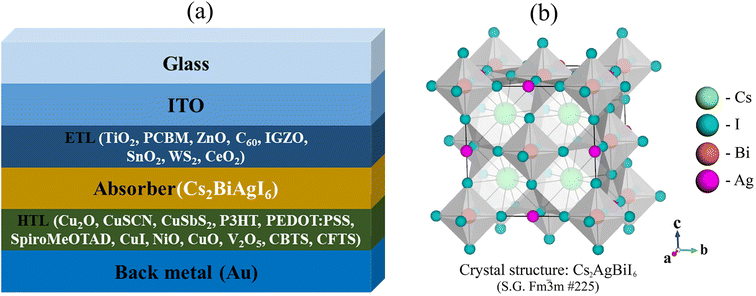 |
| | Fig. 1 (a) The design configuration of the Cs2AgBiI6-based PSC, and (b) the crystal structure of the Cs2AgBiI6 cubic-single-perovskite semiconductor. | |
2 Materials and methodology
2.1 First principal calculations of Cs2BiAgI6 absorber using DFT
This study performs the first-principle calculations exploiting the Cambridge Serial Total Energy Package (CASTEP)61 engaged in density functional theory (DFT),62 incorporating the principle of pseudo-potential plane-wave (PP-PW) total energy calculation to identify the ground state structure of Cs2AgBiI6. To grow electron–ion interactions, the Vanderbilt-type ultrasoft pseudopotential is selected.63 The exchange–correlation potential is enacted through the Generalized Gradient Approximation (GGA) composed with the Perdew–Burke–Ernzerhof (PBE) functional.64 For ensuring the convergence the cut-off energy of 520 eV is applied. The Monkhorst–Pack scheme65 is employed by taking a k-point mesh of 7 × 7 × 7, which is settled to an ultrafine mode for the first Brillouin zone. However, to see clearly the electronic charge density pattern, a larger size k-point grid (12 × 12 × 12) was used. It is also essential to apply the algorithm of Broyden–Fletcher–Goldfarb–Shanno (BFGS) during structural optimization66 so that the relatively exact lattice constants and internal atomic coordinates of Cs2AgBiI6 are assessed. It is usual to be relaxed the lattice parameters and atomic positions after structural optimization.67 The optimum converging functions to obtain the ground state structure are selected as a maximum force within 0.03 eV, maximum ionic displacement within 0.001 Å, total energy difference within 1 × 10⁻⁵ eV per atom, and maximum stress within 0.05 GPa. The electronic and optical properties are then calculated for the optimized structure by considering the aforementioned parameters.
2.2 SCAPS-1D numerical simulation
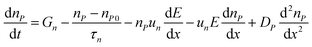
SCAPS-1D carried out the device modeling and simulation. The continuity, drift-diffusion, and position-dependent Poisson equations provide the backbone of the simulation. The three primary semiconductor equations used in the simulation framework are the continuity equations for holes (eqn (1)), electrons (eqn (2)), and the Poisson equation (eqn (3)), as shown below.68,69| |
 | (1) |
| |
 | (2) |
| |
 | (3) |
where q stands for electron charge, ε stands for dielectric permittivity, G stands for the rate of generation, D stands for the diffusion coefficient, Φ stands for electrostatic potential, E stands for the electric field, p(x) stands for the number of free holes, n(x) stands for the number of free electrons, pt(x) stands for the number of trapped holes, nt(x) stands for the number of trapped electrons, Nd+ stands for the concentration of donor-ionized doping, and Na− stands for the concentration of acceptor ionized doping, and x stands for the thickness.
2.3 wxAMPS numerical simulation
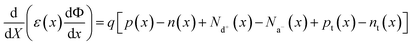
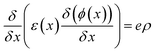
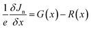
The wxAMPS, a program created by the University of Illinois, was used to do a similar numerical analysis as a secondary verification of solar cells' performance in this work.70,71 The device behavior is represented via resolving Poisson's equation (eqn (4)), which links the electrostatic potential to charge, as well as the electron and hole continuity equations (eqn (5) and (6)) in the different regions of the device structure.| |
 | (4) |
| |
 | (5) |
| |
 | (6) |
where x denotes the position, ε denotes the dielectric constant, ϕ denotes the local electric potential, e denotes the electron charge, ρ denotes the summed charge density, Jn denotes the electron current density, Jp denotes the hole electron density, G denotes the optical carrier generation rate, and R denotes the overall charge carrier recombination rate. The AMPS-1D program employs two distinct models: the lifetime model and the density of state (DOS) model. For a clear comprehension, the recombination phenomena, and changes in defect states, as well as their effects on the electric field variance across the charges transport materials/perovskite interfaces, were taken into consideration in this study using the density of state model. By resolving three-coupled non-linear differential equations with appropriate boundary conditions, the AMPS-1D can determine the quasi-Fermi level and the electrostatic potential at all locations in the device. The solar cell figures of merit can be computed in accordance with the definitions of these variables based on the device depth.
2.4 Cs2BiAgI6-based PSC structure
Here, along with the Cs2BiAgI6 absorber layer, ETL, HTL, and back contact are associated to form the structure of double perovskite solar cell. The solar cell structure of the Cs2BiAgI6 absorber forms an n–i–p structure. In this instance, an n–i–p structure's superior long-wavelength response makes it preferable to a traditional semiconductor p–n junction, and deep within the device, across the intrinsic area, the depletion zone of an n–i–p structure is present. When a cell is exposed to long wavelength radiation, photons enter the cell deeply. However, only electron–hole pairs produced in and close to the depletion area can contribute to the creation of current. An efficient creation and separation mechanisms of electron–hole pairs are made possible by the greater depletion width, which raises the cell's quantum efficiency.14 Cs2BiAgI6 captures photons due to double heterostructure it ensures the charge and photon confinement and both sides of highly doped ETL and HTL work as an ohmic contact. During the study SCAPS-1D, the software helps us to investigate the performance of various structures of double PSCs. By keeping the ambient temperature 300 K, frequency 1 MHz, and AM 1.5 G sunlight spectrum double perovskite structures are formed. Also taken eight ETLs and twelve HTLs, back contact as Au to investigate the different structures and their optoelectronic parameters are set up initially from the different studies which are mentioned in Tables 1–3.
Table 1 Input optimization parameters of the TCO, ETL, and absorber layer of the study
| Parameters |
ITO |
TiO2 |
PCBM |
ZnO |
C60 |
IGZO |
SnO2 |
WS2 |
CeO2 |
Cs2BiAgI6 |
| This study. |
| Thickness (nm) |
500 |
30 |
50 |
50 |
50 |
30 |
100 |
100 |
100 |
800a |
| Band gap, Eg (eV) |
3.5 |
3.2 |
2 |
3.3 |
1.7 |
3.05 |
3.6 |
1.8 |
3.5 |
1.6 |
| Electron affinity, X (eV) |
4 |
4 |
3.9 |
4 |
3.9 |
4.16 |
4 |
3.95 |
4.6 |
3.90 |
| Dielectric permittivity (relative), εr |
9 |
9 |
3.9 |
9 |
4.2 |
10 |
9 |
13.6 |
9 |
6.5 |
| CB effective density of states, NC (1/cm3) |
2.2 × 10¹⁸ |
2 × 10¹⁸ |
2.5 × 10²¹ |
3.7 × 10¹⁸ |
8.0 × 10¹⁹ |
5 × 10¹⁸ |
2.2 × 10¹⁸ |
1 × 10¹⁸ |
1 × 10²⁰ |
1 × 10¹⁹ |
| VB effective density of states, NV (1/cm3) |
1.8 × 10¹⁹ |
1.8 × 10¹⁹ |
2.5 × 10²¹ |
1.8 × 10¹⁹ |
8.0 × 10¹⁹ |
5 × 10¹⁸ |
1.8 × 10¹⁹ |
2.4 × 10¹⁹ |
2 × 10²¹ |
1 × 10¹⁹ |
| Electron mobility, μn (cm2 V−1 s−1) |
20 |
20 |
0.2 |
100 |
8.0 × 10⁻² |
15 |
100 |
100 |
100 |
2 |
| Hole mobility, μh (cm2 V−1 s−1) |
10 |
10 |
0.2 |
25 |
3.5 × 10⁻³ |
0.1 |
25 |
100 |
25 |
2 |
| Shallow uniform acceptor density, NA (1/cm3) |
0 |
0 |
0 |
0 |
0 |
0 |
0 |
0 |
0 |
1 × 10¹⁵a |
| Shallow uniform donor density, ND (1/cm3) |
1 × 10²¹ |
9 × 10¹⁶ |
2.93 × 10¹⁷ |
1 × 10¹⁸ |
1 × 10¹⁷ |
1 × 10¹⁷ |
1 × 10¹⁷ |
1 × 10¹⁸ |
1021 |
0a |
| Defect density, Nt (1/cm3) |
1 × 10¹⁵a |
1 × 10¹⁵a |
1 × 10¹⁵a |
1 × 10¹⁵a |
1 × 10¹⁵a |
1 × 10¹⁵a |
1 × 10¹⁵a |
1 × 10¹⁵a |
1 × 10¹⁵a |
1 × 10¹⁵a |
| Reference |
14 |
14 |
14 |
14 |
14 |
14 |
14 |
14 |
14 |
72 |
Table 2 Input optimization parameters HTL the study14
| HTL |
Cu2O |
CuSCN |
CuSbS2 |
P3HT |
PEDOT:PSS |
Spiro-MeOTAD |
NiO |
CuI |
CuO |
V2O5 |
CFTS |
CBTS |
| This study. |
| Thickness (nm) |
50 |
50 |
50 |
50 |
50 |
200 |
100 |
100 |
50 |
100 |
100 |
100 |
| Band gap, Eg (eV) |
2.2 |
3.6 |
1.58 |
1.7 |
1.6 |
3 |
3.8 |
3.1 |
1.51 |
2.20 |
1.3 |
1.9 |
| Electron affinity, X (eV) |
3.4 |
1.7 |
4.2 |
3.5 |
3.4 |
2.2 |
1.46 |
2.1 |
4.07 |
4.00 |
3.3 |
3.6 |
| Dielectric permittivity (relative), εr |
7.5 |
10 |
14.6 |
3 |
3 |
3 |
10.7 |
6.5 |
18.1 |
10.00 |
9 |
5.4 |
| CB effective density of states, NC (1/cm3) |
2 × 10¹⁹ |
2.2 × 10¹⁹ |
2 × 10¹⁸ |
2 × 10²¹ |
2.2 × 10¹⁸ |
2.2 × 10¹⁸ |
2.8 × 10¹⁹ |
2.8 × 10¹⁹ |
2.2 × 10¹⁹ |
9.2 × 10¹⁷ |
2.2 × 10¹⁸ |
2.2 × 10¹⁸ |
| VB effective density of states, NV (1/cm3) |
1 × 10¹⁹ |
1.8 × 10¹⁸ |
1 × 101 |
2 × 10²¹ |
1.8 × 10¹⁹ |
1.8 × 10¹⁹ |
1 × 10¹⁹ |
1 × 10¹⁹ |
5.5 × 10²⁰ |
5.0 × 10¹⁸ |
1.8 × 10¹⁹ |
1.8 × 10¹⁹ |
| Electron mobility, μn (cm2 V−1 s−1) |
200 |
100 |
49 |
1.8 × 10⁻³ |
4.5 × 10⁻² |
2.1 × 10⁻³ |
12 |
100 |
100 |
3.2 × 10² |
21.98 |
30 |
| Hole mobility, μh (cm2 V−1 s−1) |
8600 |
25 |
49 |
1.86 × 10⁻² |
4.5 × 10⁻² |
2.16 × 10⁻³ |
2.8 |
43.9 |
0.1 |
4.0 × 101 |
21.98 |
10 |
| Shallow uniform acceptor density, NA (1/cm3) |
1 × 10¹⁸ |
1 × 10¹⁸ |
1 × 10¹⁸ |
1 × 10¹⁸ |
1 × 10¹⁸ |
1.0 × 10¹⁸ |
1 × 10¹⁸ |
1.0 × 10¹⁸ |
1 × 10¹⁸ |
1 × 10¹⁸ |
1 × 10¹⁸ |
1 × 10¹⁸ |
| Shallow uniform donor density, ND (1/cm3) |
0 |
0 |
0 |
0 |
0 |
0 |
0 |
0 |
0 |
0 |
0 |
0 |
| Defect density, Nt (1/cm3) |
1.0 × 10¹⁵a |
1 × 10¹⁵a |
1 × 10¹⁵a |
1 × 10¹⁵a |
1 × 10¹⁵a |
1.0 × 10¹⁵a |
1 × 10¹⁵a |
1.0 × 10¹⁵a |
1 × 10¹⁵a |
1 × 10¹⁵a |
1 × 10¹⁵a |
1 × 10¹⁵a |
Table 3 Input parameters of interface defect layers14
| Interface |
Defect type |
Capture cross section: electrons/holes (cm2) |
Energetic distribution |
Reference for defect energy level |
Total density (cm−3) (integrated over all energies) |
| ETL/Cs2BiAgI6 |
Neutral |
1.0 × 10⁻¹⁷ |
Single |
Above the VB maximum |
1.0 × 10¹⁰ |
| 1.0 × 10⁻¹⁸ |
| Cs2BiAgI6/HTL |
Neutral |
1.0 × 10⁻¹⁸ |
Single |
Above the VB maximum |
1.0 × 10¹⁰ |
| 1.0 × 10⁻¹⁹ |
3 Results and discussion
3.1 Analysis of DFT results
3.1.1 Structural properties of Cs2BiAgI6 compound. According to the optimization output, the crystal structure of Cs2AgBiI6 is a cubic double-perovskite-type system with space group Fm![[3 with combining macron]](https://www.rsc.org/images/entities/char_0033_0304.gif) m (#225). The atomic positions of Cs, Ag, Bi, and I in the unit cell are 8c (0.25, 0.25, 0.25), 4a (0, 0, 0), 4b (0.5, 0.5, 0.5), and 24e (0.2513, 0, 0). The optimized three-dimensional crystal structure of Cs2AgBiI6 is projected in Fig. 1(b). The calculated lattice parameter a = 8.6338 Å is lower than that of the previously reported lattice parameter of similar double perovskite-type compound Cs2AgBiBr6 (a = 11.430 Å)59 due to the difference of atomic radius between I and Br as well as using different calculation parameters. However, the negative value of formation energy (ΔEf = −2.66 eV per atom) calculated by the following equation (eqn (7)) confirms the thermodynamic stability of optimized Cs2AgBiI6.73
m (#225). The atomic positions of Cs, Ag, Bi, and I in the unit cell are 8c (0.25, 0.25, 0.25), 4a (0, 0, 0), 4b (0.5, 0.5, 0.5), and 24e (0.2513, 0, 0). The optimized three-dimensional crystal structure of Cs2AgBiI6 is projected in Fig. 1(b). The calculated lattice parameter a = 8.6338 Å is lower than that of the previously reported lattice parameter of similar double perovskite-type compound Cs2AgBiBr6 (a = 11.430 Å)59 due to the difference of atomic radius between I and Br as well as using different calculation parameters. However, the negative value of formation energy (ΔEf = −2.66 eV per atom) calculated by the following equation (eqn (7)) confirms the thermodynamic stability of optimized Cs2AgBiI6.73| |
 | (7) |
Here, Es (Cs), Es(Ag), Es(Bi), and Es(I) are the energy of Cs, Ag, Bi, and I atoms, respectively, while Etot(Cs2AgBiI6) is the unit cell total energy of Cs2AgBiI6, and N represents the number of atoms in the unit cell.
3.1.2 Band structure and DOS of Cs2BiAgI6 compound. The electronic properties provide important information to explain materials' bonding nature, photon-absorbing behaviours, and other relevant properties.74 A compound's electronic properties are mostly related to its band structure, the density of states (DOS), and charge density. The result of band structure calculation along the highly symmetric directions within the k-space for Cs2AgBiI6 is presented in Fig. 2(a), where a red horizontal dash line at 0 eV indicates the Fermi level (EF). The bands below and above the EF are usually called the valence and conduction bands, respectively. It is observed from Fig. 2(a) that either the valence or conduction band is not crossed the EF and overlaps with each other. Hence the compound Cs2AgBiI6 has a band gap in its electronic band structure. The calculated band gap is found to be 0.846 eV. The band gap value of the studied compound is somewhat lower than that of other similar double perovskite-type compounds Cs2AgBiBr6 (2.19 eV),26 Cs2AgBiCl6 (2.77 eV),26 Cs2AgInCl6 (3.23 eV),75 and Cs2AgSbCl6 (1.40 eV).60
 |
| | Fig. 2 (a) Calculated band structure of Cs2AgBiI6 along the high-symmetry direction, (b) calculated total and partial density of states of Cs2AgBiI6, and (c) the charge density mapping of Cs2AgBiI6 along (111) crystallographic plane. | |
Moreover, the minimum conduction band and maximum valence band are observed at F- and Q-points, respectively, exhibiting the indirect semiconducting nature of double perovskite compound Cs2AgBiI6. Besides, the valence band maximum is the nearest band to the EF, which ensures the p-type semiconducting nature of chosen double perovskite. Interestingly, some nearly flat valence bands between F- and Z-points close to the EF are also observed. This highly dispersive nature of the bands near the EF indicated the high mobility of charge carriers and predicted that the effective mass would be significantly higher in these bands.
Fig. 2(b) represents the total density of state (TDOS) together with the partial density of state (PDOS), which are used to understand further the contributions of different atoms/orbitals and the chemical bonding nature in Cs2AgBiI6. In the DOS diagram, the EF is represented by the red vertical dashed line fitted at 0 eV. The TDOS diagram confirms the band gap in the electronic structure of the studied double perovskite, reflecting a similar nature as the band diagram. The valence band mainly consists of Ag-4d and I-5p states together with the minimal contributions of Cs-6s, Cs-5p, and Bi-6p orbitals. On the other hand, the conduction band in the vicinity of the EF mostly arises from the Bi-6p state. However, the conduction band over 4 eV originated from the significant contribution of I-5s with a small share of 6s and 5p states of the Cs atom. Notably, the valence band maximum at the Q-point of the Brillouin zone near the EF is generated due to the influence of the I-5p state. As a result, in the PDOS of the investigated compound, the orbital electrons of the I-5s/5p orbitals are crucial for absorbing light energy and producing conductivity.
3.1.3 Electron charge density of Cs2BiAgI6 compound. To understand and give a clear explanation of the charge transformation and nature of bonding among constituent atoms of double perovskite Cs2AgBiI6, the study of charge density mapping is crucial.54,55 The charge density mapping along the (111) crystallographic plane is illustrated in Fig. 2(c), in which the right scale shows the intensity of electron density (blue and red colors denote the highest and lowest intensity of electron density, respectively). The highest intensity of charge density is observed around the Ag atom, whereas it is lowest around the Bi atom. The charge contours of the Cs and I atoms do not overlap, indicating the existence of ionic bonding between these two atoms. A similar phenomenon is also noticed for Ag and I atoms, revealing the ionic nature of Ag–I bonds. On the other hand, the elliptical contour of charges between Bi and I atoms exhibits the presence of strong covalent bonding of Bi–I bonds. Moreover, isoline sharing suggests that a charge transfer between these two atoms may occur. The strong covalent nature of Bi–I bonds mainly originated from the hybridization between the electronic orbital states of Bi-6p and I-5p.
3.1.4 Optical properties of Cs2BiAgI6 compound. The optical functions are essential for understanding the behavior of a material when an incident electromagnetic wave interacts with it. Therefore, these functions bear crucial significance for exploring possible uses of material in photovoltaic and optoelectronic instruments. In such cases, the nature of a specific material under incident photon (infrared, visible, and ultraviolet) is necessary to examine. A number of optical processes, namely, dielectric constant ε(ω), refractive index n(ω), absorption α(ω), conductivity σ(ω), and reflectivity R(ω) are determined to investigate the response of Cs2AgBiI6 upon photon energies up to 30 eV. Generally, both the intra-band and inter-band transitions are used to calculate the ε(ω). However, the present calculation overlooks the intra-band contributions that are arisen from indirect transitions. This is because of the inclusion of phonon in the indirect intra-band transition and possesses a limited scattering cross-section76 related to the direct transition. Hence, there is no need to retain the momentum of phonon scattering. It can be seen from Fig. 3(a) that the real and imaginary parts of the dielectric function are higher at low energy and remarkably reduced in high-energy regions. This matter hints at the useful usage of Cs2AgBiI6 in microelectronic devices and integrated circuits.14 The ε(ω) is connected to electron excitement that originates predominantly because of interband transitions and exhibits minor peaks at ∼6 eV due to intraband transitions. The real and imaginary parts of n(ω) are shown in Fig. 3(b). The real part falls gradually in a similar fashion as the real part of the dielectric function, whereas the imaginary part slightly exceeds the real part at ∼9 eV and then again falls below the real part at ∼16 eV. The real part of the refractive index is relatively large at zero photon energy, and the maximum is found at ∼2 eV. It suggests the possible device applications of a chosen compound in quantum-dot light-emitting diodes, organic light-emitting diodes, solar cells, and waveguides.54,73
 |
| | Fig. 3 Calculated (a) dielectric function, (b) refractive index, (c) absorption, (d) conductivity, and (e) reflectivity of Cs2AgBiI6. | |
The α(ω) presented in Fig. 3(c) manifests the spectra around 0–26 eV owing to the transitions between energy bands. Importantly, it starts from slightly above zero energy, which reconfirms the small band gap of Cs2AgBiI6. The α(ω) is relatively higher at lower photon energy, which predicts the studied compound's potential use in solar panels. Due to the semiconducting Nature of Cs2AgBiI6, the σ(ω) also does not start at zero energy (Fig. 3(d)). It starts at ∼0.84 eV, and the maximum spectrum is attained at 6 eV, which becomes lower with increasing energy. The large conductivity at lower photon energy suggests the conventional applications of Cs2AgBiI6. It can be noticed from Fig. 3(e) that the static reflectivity R(0) is ∼21% of total radiation, which is increased in the high-energy region because of inter-band transitions. Moreover, the R(ω) exhibits lower values (<44%) over the studied energy range, indicating significant absorptivity/transmissivity of light, which means that this compound may absorb a significant number of photons and making it suitable for use in optoelectronic devices.54
3.2 Analysis of SCAPS-1D results
3.2.1 Effect of HTL layer. In the PSCs device configuration, HTL collects holes from the perovskite (Cs2BiAgI6) and then transfers them to the back metal contact (Au). Twelve types of HTL have been utilized in SCAPS-1D simulation to optimize the device's performance (Table 2). The visual depiction of the HTL optimization process is shown in Fig. 4. Fig. 4(a) illustrates that PCBM as ETL is optimized with CBTS as HTL compared to the other HTL, while the PCE of this perovskite device configuration is 19.99%. Besides, TiO2 as ETL showed maximum optimization with CBTS as HTL in Fig. 4(b), with a PCE of 21.55%. Fig. 4(c) demonstrates that ZnO as ETL with CBTS as HTL exhibited more optimization than other HTL, with a PCE of 21.59%. Similarly, SnO2, IGZO, and WS2 as ETL with CBTS as HTL demonstrated the highest optimization compared to other HTLs. The PCEs of these device configurations are 21.52%, 20.42%, and 21.43% respectively (Fig. 4(d), (e), and (f)). And the C60 and CeO2 as ETL with CBTS as HTL showed the best optimization than other HTLs, with PCE of 17.47% and 14.44%, respectively. Compared to the other HTL presented in this study, CBTS exhibited the highest performance with different ETL. Therefore, CBTS is suitable for HTL optimization among numerous simulated device configurations.
 |
| | Fig. 4 Variation of performance parameters, i.e., VOC (V), JSC (mA cm−2), FF (%), and PCE (%) of Cs2BiAgI6 absorber layer-based PSCs device for different HTLs with Au as back metal contact and ETLs of (a) PCBM, (b) TiO2, (c) ZnO, (d) SnO2, (e) IGZO, and (f) WS2. | |
3.2.2 ETL optimization. In the PSCs device configuration, ETL removes the electron from the perovskite materials and then transfers the electron to the ITO. ETL also prevent electron in ITO from recombining with the absorber layer's holes.77 Simulating each ETL with different HTL in the Cs2BiAgI6 perovskite absorber optimizes the performance of device configuration (Tables 1 and 2). In this study, we used electron transport materials (ETMs) such as TiO2, PCBM, ZnO, C60, IGZO, SnO2, WS2, and CeO2 with different electron transport materials (HTMs). After simulating all possible combinations between the ETM layer and HTM layer with Cs2BiAgI6 absorber and Au metal contact, all ETL showed maximum optimization with CBTS as HTL. As a result, eight sets of device configurations from ninety-six combinations exhibited maximum optimized performance and efficiency of device configurations. While band alignment of ZnO (3.3 eV), TiO2 (3.2 eV), and SnO2 (3.6 eV) ETL was significantly higher in comparison with other ETLs which showed ≳21.5% efficiency with CBTS HTL (Fig. 5). On the contrary, CeO2 (3.5 eV) band alignment isn't convenient with the Cs2BiAgI6 absorber and CBTS HTL which performed an efficiency of 14.44%. Table 4 illustrates the performance parameters VOC, JSC, FF, and PCE, which exhibited good agreement value in these eight device configurations.
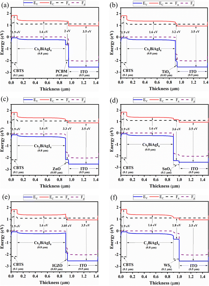 |
| | Fig. 5 Energy band diagram of solar cells structure with different ETMs of (a) PCBM, (b) TiO2, (c) ZnO, (d) SnO2, (e) IGZO, and (f) WS2. | |
Table 4 Optimized performance parameters of the best combination for each of the ETLs and HTLs
| Optimized device |
Cell thickness (μm) |
VOC (V) |
JSC (mA cm−2) |
FF (%) |
PCE (%) |
| ITO/PCBM/Cs2BiAgI6/CBTS/Au |
0.5/0.05/0.8/0.1/Au |
1.081 |
22.39 |
82.56 |
19.99 |
| ITO/TiO2/Cs2BiAgI6/CBTS/Au |
0.5/0.03/0.8/0.1/Au |
1.084 |
23.80 |
83.61 |
21.55 |
| ITO/ZnO/Cs2BiAgI6/CBTS/Au |
0.5/0.05/0.8/0.1/Au |
1.085 |
23.76 |
83.78 |
21.59 |
| ITO/C60/Cs2BiAgI6/CBTS/Au |
0.5/0.05/0.8/0.1/Au |
1.077 |
19.62 |
82.65 |
17.47 |
| ITO/IGZO/Cs2BiAgI6/CBTS/Au |
0.5/0.03/0.8/0.1/Au |
1.092 |
23.66 |
79.04 |
20.42 |
| ITO/SnO2/Cs2BiAgI6/CBTS/Au |
0.5/0.1/0.8/0.1/Au |
1.084 |
23.77 |
83.54 |
21.52 |
| ITO/CeO2/Cs2BiAgI6/CBTS/Au |
0.5/0.1/0.8/0.1/Au |
0.924 |
23.59 |
66.21 |
14.44 |
| ITO/WS2/Cs2BiAgI6/CBTS/Au |
0.5/0.1/0.8/0.1/Au |
1.085 |
23.54 |
83.91 |
21.43 |
3.2.3 Band diagram. The energy band diagram utilizes each ETL with a Cs2BiAgI6 absorbing layer and CBTS as HTL influencing valence/conduction band offset (i.e., valence band difference between HTL and the absorber layer and conduction band between ETL and absorber layer). The alignment of the energy levels has a significant impact on the efficiency and performance of the PSCs. In the PSCs, photo-generated electrons are injected into the ETL conduction band, and at the same time, holes are transported to the HTL. Afterward, electrons and holes are collected at their respective front (ITO) and back contact metal (Au) correspondingly. The energy band mismatch at the ETL/Cs2BiAgI6 and the Cs2BiAgI6/HTL interface significantly impacts the device's performance parameters. The nature of the interface controls the effect of interfacial recombination. Therefore, carefully tuning the electronic properties of ETL and HTL materials became a vital task. Thus, the electron affinity of ETL should be higher than that of Cs2BiAgI6 to extract the electron safely at the ETL/Cs2BiAgI6 interface, and the ionization energy of HTL should be lower than that of Cs2BiAgI6 to extract the holes at the Cs2BiAgI6/HTL interface. Fig. 5 shows that the Fermi level, which is near the conduction band, enters into the conduction band in the case of the best eight sets of Cs2BiAgI6-based device configuration. The PCBM as ETM layer and CBTS as HTM layer associated with Cs2BiAgI6-based device configuration showed that the Fermi level crossed the conduction band, as shown in Fig. 5(a). Fig. 5(c)–(h) exhibited the others of Cs2BiAgI6-based perovskite device configurations where TiO2, ZnO, C60, IGZO, SnO2, WS2, and CeO2 as ETL and CBTS as HTL showed the same pattern and degenerate semiconductors nature as like Fig. 5(a).
3.2.4 Effect of absorber and ETL thickness on cell performance. The effect of the absorber layers and different ETL layer thicknesses of desired eight double perovskites solar cell structures are investigated through contour plot mapping to evaluate the solar cell's performance parameters. An appropriate absorber and ETL selection of any solar cell is the primary and crucial element in achieving high-performance solar cells. Moreover, the appropriate thickness of the absorber and ETL helps to capture the light and collect holes from the absorber layer, accordingly. Fig. 6 represents the effect of ETL and absorber layer thickness on the VOC parameter of the eight most efficient solar cell structures enlisted in Table 4. From Fig. 6(a), it is observed that ETL thickness is 0.1 μm and absorber thickness is in the range of 0.4 μm in the case of ETL as a PCBM-associated structure. In addition, simultaneously increasing ETL thickness with absorber layer thickness can cause lower VOC (Fig. 6(a)). For the TiO2 and ZnO as ETL-associated structures, the thickness of the absorber layer remains constant with increasing ETL layer thickness (Fig. 6(b) and (c)). The highest value of VOC for TiO2 and ZnO as ETL-associated structures are exhibited at around 0.3 μm and 0.5 μm absorbers layer thickness regardless of ETL thickness (Fig. 6(b) and (c)). For the C60 as ETL associated structure, the highest VOC is exhibited when absorber thickness is around 0.4 μm, and ETL thickness is about 0.1 μm (Fig. 6(d)). On the other hand, for IGZO as ETL, the higher VOC value is shown when the absorber layer is <0.4 μm with regardless of the ETL layer thickness (Fig. 6(e)). The SnO2 as ETL-associated solar cell structure shows VOC at a similar range at a particular absorber layer thickness, which is 0.5 to 0.6 μm (Fig. 6(f)). The VOC values of CeO2 as an ETL-associated solar cell structure are shown between 0.1 to 0.2 μm ETL thickness and 0.4 to 0.5 μm absorber layer thickness (Fig. 6(g)). According to Fig. 6(h), WS2 as an ETL-associated solar structure shows a higher VOC at around 0.03 to 0.25 μm of ETL thickness and 0.3 to 0.4 μm absorber thickness. In conclusion, the larger thickness of the absorber layer might be the cause of lower VOC for most of the studied solar structures, as observed in Fig. 6. This fact is explained by the increase in carrier recombination rate in the presence of a thick absorber layer, causing a rise in saturation current larger than photocurrent.
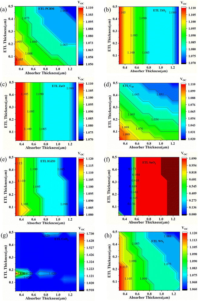 |
| | Fig. 6 Contour mapping of VOC (V) when ETL as (a) PCBM, (b) TiO2, (c) ZnO, (d) C60, (e) IGZO, (f) SnO2, (g) CeO2, and (h) WS2. | |
Fig. 7 represents the effect of variation of ETL and absorber layer thickness on the JSC parameter of eight desired perovskite solar cells. For PCBM as an ETL-associated solar cell, the maximum JSC (22.08 to 24 mA cm−2) value is exhibited when the ETL thickness is 0.03 to 0.1 μm and the absorber thickness is 0.6 to 1.3 μm (Fig. 7(a)). The almost similar pattern we have observed for ETL C60 – associated solar cells, where the higher JSC (19.74 to 22.10 mA cm−2) value is observed when absorber thicknesses are from 0.6 to 1.3 μm and ETL thicknesses are from ≤0.1 μm (Fig. 7(d)). It is observed that the lower ETL thickness and higher absorber thickness can cause higher JSC. Higher absorber thickness permits more light collection and hence increases the generation rate, giving a high JSC value. Thin ETL can boost the current via decreasing electron–hole pair recombination which reduces the effect of series resistance. Besides, minimizing the ETL thickness prevents the formation of wider pinholes and rough terrain surfaces, which can severely impede the JSC, VOC, and therefore efficiency. The maximum JSC value for TiO2 as ETL and ZnO as ETL-associated solar structures are shown to be the same when the absorber layer thicknesses are 0.8 to 1.3 μm, and ETL thickness doesn't make any significant effect during the variation (Fig. 7(b) and (c)). From Fig. 7(e), we observe that IGZO as ETL associated solar cell structure shows a maximum JSC pattern, which is almost 24 mA cm−2 when absorber thickness is 0.8 to 1.3 μm, and ETL thickness is 0.03 to 0.3 μm. The SnO2 as an ETL-associated solar structure shows a moderate JSC pattern range with the absorber and ETL thickness variation (Fig. 7(f)). In the case of CeO2 as ETL, the maximum JSC is 23.58 to 24.20 mA cm−2 when absorber thickness is about 0.8 to 1.3 μm, regardless of ETL thickness (Fig. 7(g)). Finally, WS2 as an ETL-associated solar cell shows the highest JSC (24.50 mA cm−2) pattern when absorber thickness is 0.7 to 1.3 μm and ETL thickness is 0.03 to 0.2 μm (Fig. 7(g)).
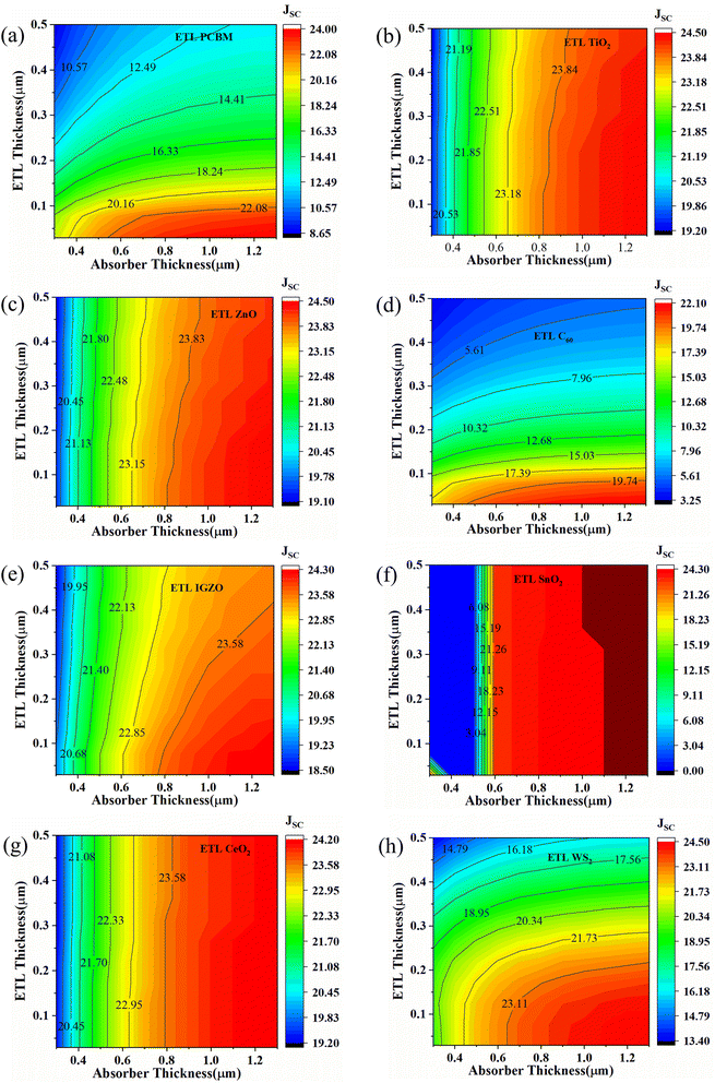 |
| | Fig. 7 Contour mapping of JSC (mA cm−2) when ETL as (a) PCBM, (b) TiO2, (c) ZnO, (d) C60, (e) IGZO, (f) SnO2, (g) CeO2, and (h) WS2. | |
The effect on FF values for the variation of absorber and ETL layer thickness is shown in Fig. 8. For PCBM as an ETL-associated solar structure, it is observed that FF values are decreased with increased absorber and ETL layer thickness (Fig. 8(a)). This fact is due to the increased series resistance. The lowest FF is observed at around 79.16%, as shown in Fig. 8(a). A similar pattern is observed for TiO2, ZnO, C60, IGZO, and WS2-associated solar structures (Fig. 8(b)–(e), and (h)). However, Fig. 8(f) shows that when SnO2 is an ETL, the FF values are observed from 31 to 50%. In contrast, the FF values for CeO2 as ETL-associated solar cells are increased with decreased absorber thickness (Fig. 8(g)). An anomaly of the FF pattern is observed for different ETL layer thicknesses (around 0.03–0.5 μm) with different absorber layers (Fig. 8(g)).
 |
| | Fig. 8 Contour mapping of FF (%) when ETL as (a) PCBM, (b) TiO2, (c) ZnO, (d) C60, (e) IGZO, (f) SnO2, (g) CeO2, and (h) WS2. | |
Fig. 9(a) and (d) show that PCBM and C60, as ETL-associated solar cells exhibit the same pattern with increasing absorber and ETL layer thickness. The highest PCE of PCBM and C60 as ETL is 20.90% and 19.30% when the ETL thickness is less than 0.7 μm and the absorber layer thickness is 0.4 to 1.3 μm. The TiO2 and ZnO as ETL-associated solar cells show the same pattern for PCE with increasing ETL and absorber layer thickness (Fig. 9(b) and (c)). The highest PCE is observed when the absorber layer thickness is more than 0.6 μm regardless of ETL thickness, as shown in Fig. 9(b) and (c). For IGZO as ETL, the maximum PCE (20.40%) is observed when the absorber layer thickness is 0.5 to 1.1 μm and the ETL layer thickness is 0.03 to 0.1 μm (Fig. 9(e)). The PCE pattern is almost moderate in the case of SnO2 as an ETL-associated solar structure (Fig. 9(f)). For CeO2 as ETL, the highest PCE is observed when absorber thickness is 0.5 to 0.7 μm, and ETL thickness does not significantly impact the PCE pattern, as shown in Fig. 9(g). Finally, in the range of 0.5 to 1.5 μm absorber and less than 0.15 μm ETL thickness, the PCE is highest for WS2 as an ETL-associated solar structure (Fig. 9(h)).
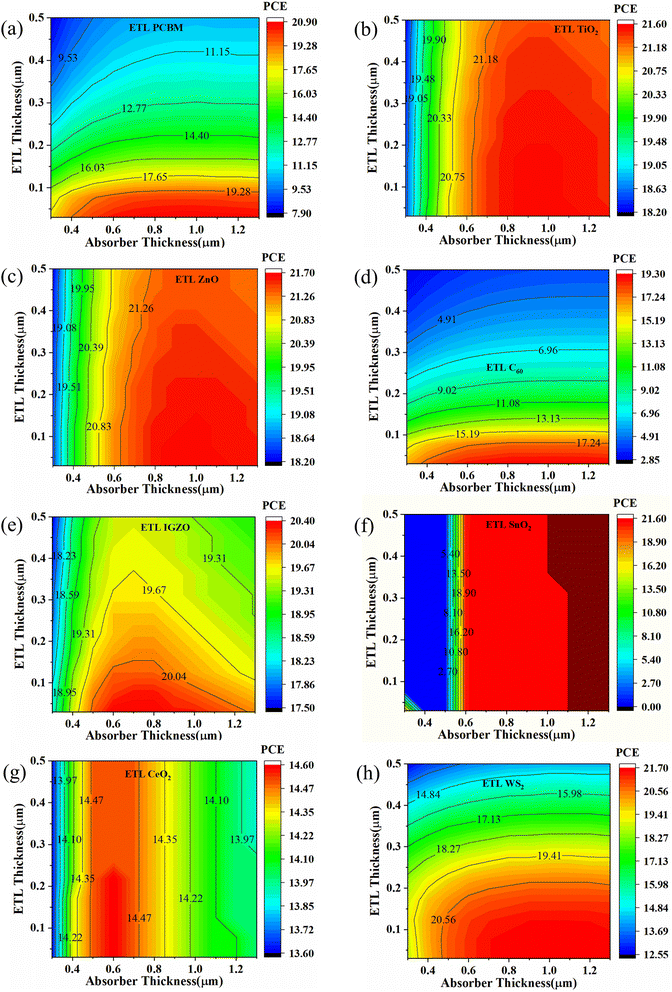 |
| | Fig. 9 Contour mapping of PCE (%) when ETL as (a) PCBM, (b) TiO2, (c) ZnO, (d) C60, (e) IGZO, (f) SnO2, (g) CeO2, and (h) WS2. | |
The changing trend of VOC, JSC, FF, and PCE of perovskite solar cells with different ETL is very distinct due to several reasons. The absorption coefficient significantly affects the PV parameters like VOC, JSC, FF, and PCE and is directly linked with the bandgap of the ETLs. It also affects the coupling of incident photons in the underlying Cs2BiAgI6 absorber layer. The conduction band offset (CBO) which depends on the work function (affinity + fermi energy level) difference between ETL and absorber layer may also play a crucial role in the performance of the solar cell. Where there is a preferred electron affinity, it can have a big impact on how well the solar cell works. Energy cliffs with CBO (−) and energy spikes with CBO (+) are produced when the electron affinities of the ETL and absorber layers are different. In other words, if the position of the conduction band (CB) of the ETL is lower than the absorber, the energy cliff CBO (−) is formed at the ETL/absorber interface without the potential to act as an electron barrier.78 So, PCBM, C60, and CeO2 have no electron barrier on the ETL/absorber interface. On the contrary, if the energy spike-CBO (+) is formed at the ETL/absorber interface it will act as an electron barrier.78 Therefore, ETLs like TiO2, ZnO, IGZO, SnO2, and WS2 have electron potential barriers at the ETL/absorber interface. Such kind of spike structure developed at the ETL/absorber layer interface, which can operate as a barrier for photo-generated electron flow towards the edge of the ETL/absorber, has the advantage of enhancing the photo generation of free charge carriers.
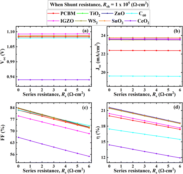
Additionally, by doing this, the rate of recombination at the contact will be reduced, improving PV performance. The primary recombination process occurs at the interface when the activation energy for carrier recombination (EA) is lower than the bandgap of the absorber layer, as opposed to the creation of cliff structures between ETL and perovskite. Additionally, the development of “cliff-type” band alignment will lower the resistance to electron transfer, resulting in a fall in EA, which directly influences the value of VOC and, in turn, the PV parameters like JSC, FF, and PCE of the solar cell.79 The impact of CBO on VOC can be described according to eqn (8) and (9) where VOC denotes open circuit voltage, EA denotes the activation energy, n denotes the diode ideality factor, K denotes Boltzmann constant, T denotes temperature, J00 denotes current pre factor and JSC denotes short circuit current density:
| |
 | (8) |
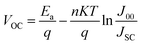
3.2.5 Effect of series resistance. The performance of solar cells is significantly impacted by the shunt (RSh) and series (Rs) resistances, which are produced mainly by connections among the solar cell layers, right and left side metal contacts, and manufacturing flaws.14 According to Fig. 10, the effect of RS varied from 0–6 Ω cm2 while the shunt resistance was constant at 105 Ω cm2 in the case of eight double perovskites (ITO/ETL/Cs2BiAgI6/CBTS/Au) devices. During the RS variation, PCE was decreased for all eight Cs2BiAgI6 perovskite device structures. The PCE value of SnO2, ZnO, WS2, and TiO2 as ETL-based Cs2BiAgI6 perovskite device structure decreased from around 21.60 to 19.30%. In contrast, PCBM and IGZO as ETL-based Cs2BiAgI6 perovskite device structure decreased from about 20 to 19% with increasing RS. And C60 and CeO2 ETL-associated solar cell structures, showed almost 17.5 to 16% and 14.5 to 12% PCE, respectively with the increase of RS. FF value also decreased with the increase of RS while the FF value of all ETL-associated solar cells exhibited a higher value except IGZO and CeO2 as ETL. The JSC and VOC performance showed the constant value for all ETL-associated device configurations with increasing RS. That means RS variation does not impact the JSC and VOC parameters for the studied device configurations.
 |
| | Fig. 10 Effect of RS on performance parameters ((a) VOC, (b) JSC, (c) FF, and (d) PCE) of (ITO/ETL/Cs2BiAgI6/CBTS/Au, ETL = PCBM, TiO2, ZnO, C60, IGZO, WS2, SnO2, and CeO2) double PSCs. | |
From Fig. 10(b) is seen that the current remains constant with the larger series resistance. CH3NH3SnI3-based study the performance was analyzed by varying RS from 0 to 6 Ω cm2 while keeping Rsh fixed at 105 Ω cm2 performed a similar trend of results where the current was unaffected by series resistance, reported by Sunny et al.80 Another study reported that FAPbI3, FA0.85Cs0.15PbI3, and FA0.85Cs0.15Pb(I0.85Br0.15)3-based perovskites, RS didn't affect much the current for a certain range of 30 Ω cm2. After this range, RS of ≥ 30 Ω cm2 currents for those particular devices tended to decline.81 RS is the sum of resistances between various terminals like absorber, ETL, and HTL as well as the front and back contacts of the cell which doesn't affect current up to a certain range. So, it could be concluded that the current of the Cs2BiAgI6 perovskite was affected by various studied ETLs after the larger series of resistance above 30 Ω cm2, which is in line with previous studies.
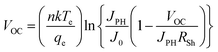
3.2.6 Effect of shunt resistance. Internal resistances, interface barriers, charge-collecting interlayers, and metal-based electrodes, are the source of RS in PSCs, whereas leakage channels, like pinholes in the photoactive layer and recombination losses, are the source of the RSh.82 The Shockley equation is expressed as eqn (10) and (11), describe the expected behavior of the J–V characteristic of a solar cell during ideal one-sun illumination conditions.83| |
 | (10) |
| |
 | (11) |
where, qeis the elementary charge, JPHis the photocurrent density, J0 is the density of the reverse bias saturation current, Rs is the series resistance, RSh is the shunt resistance, n is the diode ideality factor, k is the Boltzmann constant (1.38 × 10²³ J K−1), and Teis the ambient temperature (298 K). Also, from eqn (8) and (9), it is seen that JSC and VOC show negative inverse relation with RSh. That means with increasing RSh, JSC, and VOC's increment happens.The effect of VOC, JSC, FF, and PCE values with RSh variation is visually represented in Fig. 11, where RSh varied from 101 to 107 Ω cm2 for all eight optimum solar cell structures. The VOC, JSC, FF, and PCE values showed a similar pattern with increasing shunt resistance RSh. All performance parameters increased rapidly from 101 Ω cm2 to 103 Ω cm2 and then maintained the constant value with increasing RSh. The CeO2 as ETL associated structure showed the lowest value where CeO2 initially increased and remained constant for VOC, FF, and PCE from 0.25 V, 24%, and 2.5% to 0.9 V, 65%, and 13%, respectively, as shown in Fig. 11. In Fig. 11(b), The C60 exhibited the lowest value for JSC, from 18.5 to 19.5 (mA cm−2). The ZnO, PCBM, TiO2, IGZO, SnO2, C60, and WS2 as ETL-associated solar cell structures showed an almost similar and constant value of VOC, which is 1.1 V after RSh of 103 Ω cm2. The JSC value of TiO2, ZnO, IGZO, SnO2, WS2, and CeO2 as ETL-associated solar cell structure showed 21.0 (mA cm−2) initially and then increased to 23.5 (mA cm−2) and remained constant (Fig. 11(b)).
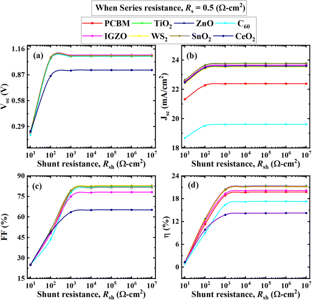 |
| | Fig. 11 Effect of RSh on performance parameters ((a) VOC, (b) JSC, (c) FF, and (d) PCE) of (ITO/ETL/Cs2BiAgI6/CBTS/Au, ETL = PCBM, TiO2, ZnO, C60, IGZO, WS2, SnO2, and CeO2) double PSCs. | |
3.2.7 Effect of temperature. One of the most important factors in determining the stability of solar cell performance is having a thorough understanding of solar cell performance at high operating temperatures. Due to the distortion between layers at high temperatures, the performance of the majority of solar cell architectures exhibits instability. Recent studies on perovskites-based optoelectronics have shown improvements in the device's performance stability at high temperatures.84–86 The temperature range has been adjusted from 275 K to 475 K to investigate the relationship between temperature and the efficiency of the solar cell. Fig. 12(a), (c), and (d) shows PCE, FF, and VOC values are decreased with increasing temperature for almost all optimum solar cell structures.
 |
| | Fig. 12 Effect of temperatures on performance parameters ((a) VOC, (b) JSC, (c) FF, and (d) PCE) of (ITO/ETL/Cs2BiAgI6/CBTS/Au, ETL = PCBM, TiO2, ZnO, C60, IGZO, WS2, SnO2, and CeO2) double PSCs. | |
In contrast, JSC remained almost constant for all optimum device configurations with temperature variation (Fig. 12(b)). The C60 as an ETL-associated solar cell showed a lower JSC of 20 mA cm−2. The PCBM as an ETL-associated structure demonstrated almost 22 mA cm−2 of JSC value, which is higher than the C60. The other ETLs with device configurations exhibited around 23.5 mA cm−2 of JSC value with increasing temperature. The VOC value was decreased from 1.16 to 0.70 V with increasing temperature for all studied device configurations except CeO2 as ETL associated device, which decreased from 0.92 to 0.72 V (Fig. 12(a)). The FF value decreased from around 85 to 74% for all optimum device configurations except IGZO and CeO2 ETL-associated devices. The PCE decreased for all devices with the increasing temperature. However, the VOC value decreased for all optimum device configurations with increasing temperature due to the inverse relationship between VOC, and the reversed saturation current density, J0. The J0 increased at a higher temperature. Eqn (12) shows the relation between VOC and J0.
| |
 | (12) |
where,

stands for the thermal voltage, and A stands for the ideality factor.
In addition, when the temperature of the PSC rises, the flaws become worse, and the VOC value decrease which is consistence with previous studies.14 From Fig. 12(b), it is evident that the current was affected slightly due to the reduction of bandgap with the increase in temperature. But the range of change is very marginal which seems to be constant during the increment of temperature. And, CH3NH3SnI3 perovskite showed a similar kind of trend of change in current with an increase in temperature from 260 K to 473 K.80 In these circumstances, the bandgap reduction could be less of being double perovskite such kind of a slight current change for temperature change.
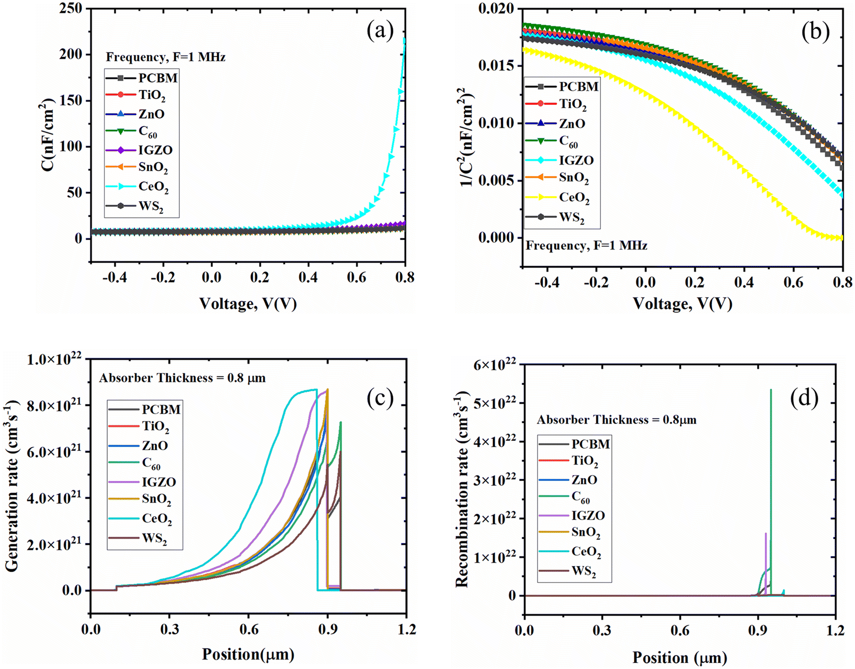
3.2.8 Effect of capacitance and Mott–Schottky. Fig. 13(a) and (b) show the Mott–Schottky (M–S) plots and the plots of capacitance per unit area (C) with bias voltage (V), respectively, for eight suitable solar cells. The built-in voltage (Vbi) and charge carrier density (Nd) can be extracted from C–V measurements by using the well-known M–S analysis experimental method. It is used in traditional semiconductor devices that contain p–n and semiconductor/metal junctions with fixed depletion layers and space charge regions. Eqn (13) yields the junction capacitance per area (C) value.| |
 | (13) |
Here, ε0 is the vacuum permittivity, εr is the donor's dielectric constant, q is the electronic charge, and V is the applied voltage (Fig. 13(b)).87,88 Nd is generated from the gradient of the linear component, and Vbi is generated from an extension of the linear part to the voltage axis. The CeO2 ETL-associated device shows voltage-independent capacitance from −0.4 V to 0.5 V, and an exponentially increasing pattern has been shown after 0.5 V (Fig. 13(a)). Whereas other ETL-associated solar structures represent the independent voltage capacitance it may be because of the saturation of depletion layer capacitance, as seen in Fig. 13(a). In the case of CeO2 as ETL associated structure Vbi shows declining in nature where ZnO, C60, PCBM, SnO2, TiO2, and WS2 as ETL associated structure shows a higher voltage.
 |
| | Fig. 13 (a) Capacitance (C), (b) Mott–Schottky (1/C2) plot, (c) generation rate, and (d) recombination rate for eight studied structures. | |
3.2.9 Effect of generation and recombination rate. Fig. 13(c) and (d) show the generation and recombination rates, respectively. The electron–hole pairs are created during the carrier generation process when an electron is excited from the valence band to the conduction band, producing a hole in the valence band. The emission of electrons and holes brings on carrier generation. To determine the creation of electron–hole pairs G(x), SCAPS-1D employs the incident photon flux Nphot(λ,x). From this photon flux for each position and wavelength, the value of G(x) can be computed through eqn (14).| | |
G(λ,x) = α(λ,x)Nphot(λ,x)
| (14) |
The process of recombination is the opposite of the process of generation, in which the electrons and holes of the conduction band are coupled and annihilated. The charge carrier's lifespan and density determine the solar cell's recombination rate. First, the electron–hole recombination is decreased because of the defect states present within the absorber layer. Then, the energy states are produced, which impacts the electron–hole recombination profile within the solar cell structure. Due to flaws and grain boundaries, the recombination rate distribution is not uniform, as shown in Fig. 13(d).54
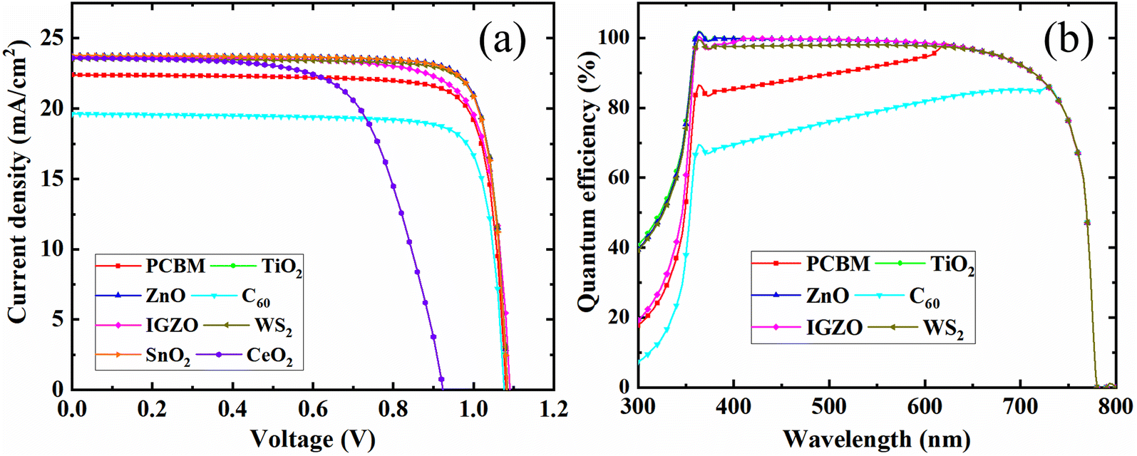
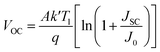
3.2.10 J–V and QE characteristics. Fig. 14(a) shows the J–V characteristics changing pattern of the studied eight solar cell structures. According to Fig. 14(a), it is noticed that C60 as an ETL-associated PSC showed about 19 mA cm−2 as current density, while the VOC is more significant than one volt. However, CeO2 as an ETL-associated device exhibited a JSC of about 23 mA cm−2 although the VOC was less than 1.0 V. However, the other ETLs associated structures showed better performance than C60 and CeO2 as ETL-associated device structures. The ZnO as ETL-associated structure demonstrated 23 mA cm−2 with unity open circuit voltage density, as shown in Fig. 14(a). The defect amount in perovskite films is a critical factor in determining the device's performance since the photoelectrons are produced in these layers. However, the electron–hole recombination behaviors are essential in defining the photovoltaic parameters of the PSC. The J–V curve in a perovskite film is shown in Fig. 14(a) as a function of bulk trap density. All photovoltaic parameters are drastically reduced when defect states are present in perovskite films. This is consistent with the observation that significant crystallinity in perovskite reduces charge recombination and enhances performance.44
 |
| | Fig. 14 (a) J–V characteristics and (b) QE curve of the double PSCs. | |
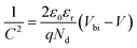
Fig. 14(b) shows the quantum efficiency (QE) curve with respect to a different wavelength. The C60 as ETL with PSC showed the optimum QE of 80% when the wavelength was almost 700 nm. The optimum QE of PCBM as an ETL-associated solar cell structure exhibited around 95% at around 620 nm. In addition, the other four ETL-associated PSCs demonstrated the highest QE of around 100% at 350 nm. Fig. 14(b) shows that the six sets of PSCs do not have QE above 800 nm. However, because of recombination, where charge carriers cannot pass into an external circuit, the QE for most solar cells is decreased. The QE is impacted by the same processes that impact collection probability. For instance, altering the front surface might impact carriers produced close to the surface. Free carrier absorption, which lowers QE in longer wavelengths, may also be brought on by highly doped front surface layers.89
3.3 Comparison with wxAMPS simulation results and previous work
3.3.1 Comparison between SCAPS-1D and wxAMPS results. A comparison of Cs2BiAgI6-based double perovskite solar cells is conducted in this section. Table 5 gives a comparative view of the performance parameters of eight Cs2BiAgI6 base solar cell structures found by optimizing different ETL and HTL from numerous simulations. PCBM as ETL associated with Cs2BiAgI6 based perovskite solar structure shows 19.99% of PCE in SCAPS-1D simulator whereas 20.70% of PCE in wxAMPS simulator (Table 5). In addition, TiO2 as ETL associated with Cs2BiAgI6-based solar cells shows 21.55% of PCE while 23.06% of PCE in the wxAMPS simulator. ZnO as an ETL-associated solar cell structure shows 21.59% PCE when SCAPS-1D is used, whereas wxAMPS shows 22.04% PCE. Similarly, C60, IGZO, SnO2, CeO2, and WS2 as ETL-associated Cs2BiAgI6-based solar cell structures show 17.47%, 20.41%, 21.52%, 14.44%, 21.43% of PCE in SCAPS-1D simulator however in wxAMPS simulator, the PCE values show 21.03%, 22.38%, 21.93%, —, 21.23%. In the case of VOC, PCBM as an ETL-associated structure shows 1.08 V in the SCAPS-1D simulator. In contrast, in the wxAMPS simulator, the device structure shows 1.18 V. Like PCBM as ETL associated structure, both simulator shows similar pattern results for VOC for all device configurations. In addition, the performance parameters JSC and FF in SCAPS-1D and wxAMPS simulator show the closest pattern for all device structures. Comparing the performance parameters of the eight solar cell structures, SCAPS-1D and wxAMPS simulators show the nearest results except for PCE and VOC, where wxAMPS shows a little higher result than SCAPS-1D (Table 5). The obtained performance parameters result from both simulators help us to understand the charges transport layers and absorber materials that are suitable for device configuration. Since both simulators give the closest performance results for eight sets of optimum solar device configurations, the presented results are reliable for further investigation which is consistent with previous studies.40,90
Table 5 Comparison between SCAPS 1D and wxAMPS software simulation
| Device structure |
Software |
VOC (V) |
JSC (mA cm−2) |
FF (%) |
PCE (%) |
| ITO/PCBM/Cs2BiAgI6/CBTS/Au |
SCAPS-1D |
1.08 |
22.39 |
82.56 |
19.99 |
| wxAMPS |
1.18 |
20.86 |
84.21 |
20.70 |
| ITO/TiO2/Cs2BiAgI6/CBTS/Au |
SCAPS-1D |
1.08 |
23.8 |
83.61 |
21.55 |
| wxAMPS |
1.18 |
23.00 |
84.69 |
23.06 |
| ITO/ZnO/Cs2BiAgI6/CBTS/Au |
SCAPS-1D |
1.085 |
23.76 |
83.78 |
21.59 |
| wxAMPS |
1.18 |
21.97 |
84.81 |
22.04 |
| ITO/C60/Cs2BiAgI6/CBTS/Au |
SCAPS-1D |
1.07 |
19.62 |
82.65 |
17.47 |
| wxAMPS |
1.18 |
21.09 |
84.73 |
21.03 |
| ITO/IGZO/Cs2BiAgI6/CBTS/Au |
SCAPS-1D |
1.09 |
23.65 |
79.04 |
20.42 |
| wxAMPS |
1.19 |
22.87 |
82.02 |
22.38 |
| ITO/SnO2/Cs2BiAgI6/CBTS/Au |
SCAPS-1D |
1.08 |
23.76 |
83.54 |
21.52 |
| wxAMPS |
1.18 |
21.94 |
82.62 |
21.93 |
| ITO/CeO2/Cs2BiAgI6/CBTS/Au |
SCAPS-1D |
0.92 |
23.59 |
66.21 |
14.44 |
| wxAMPS |
— |
— |
— |
— |
| ITO/WS2/Cs2BiAgI6/CBTS/Au |
SCAPS-1D |
1.08 |
23.53 |
83.91 |
21.43 |
| wxAMPS |
1.18 |
21.16 |
84.94 |
21.23 |
3.3.2 Comparison of SCAPS-1D results with previous work. Table 6 compares the performance parameters of the presented eight device configurations with recently published optimum configurations. Table 6 shows that the presented optimum Cs2BiAgI6 double perovskite-based solar cell shows a higher PCE value than the previously published Cs2BiAgX6 device structure. Presented eight sets of device structures PCE are 19.99%, 21.55%, 21.59%, 20.42%, 21.52%, 21.43%, 17.47%, and 14.44% whereas previously published device structures such as FTO/PCBM/Cs2BiAgI6/PTAA/Au structure shows almost 16.23% PCE,72 FTO/TiO2/Cs2BiAgI6/spiro-OMeTAD/Au structure shows around 2.43% PCE.91 The VOC values of the presented solar structures are compatible with published device configurations. In contrast, the JSC and FF values of the presented solar structure are higher than those of the previously published Cs2BiAgX6-base device structure. All presented solar structure shows JSC of greater than 19 mA cm−2, whereas earlier published device structure shows the lowest JSC value except FTO/PCBM/Cs2BiAgI6/PTAA/Au structure. Table 6 shows that the presented eight solar structures are shown more effective performance than the previously reported Cs2BiAgX6-based solar cells.
Table 6 The comparison of PV parameters of Cs2BiAgI6 and similar absorbers-based solar cells
| Typea |
Device structure |
VOC (V) |
JSC (mA cm−2) |
FF (%) |
PCE (%) |
Year |
Ref. |
| E = experimental, T = theoretical. This work. |
| E |
FTO/c-TiO2/mTiO2/Cs2AgBiBr6/N719/spiro-OMeTAD/Ag |
1.06 |
5.13 |
— |
2.84 |
2020 |
92 |
| E |
FTO/TiO2/Cs2AgBiBr6/spiro-OMeTAD/Au |
0.98 |
3.96 |
62.40 |
2.43 |
2021 |
91 |
| T |
FTO/PCBM/Cs2BiAgI6/PTAA/Au |
1.08 |
19.94 |
74.87 |
16.23 |
2021 |
72 |
| T |
Ohmic contact/spiro-OMeTAD/Cs2BiAgI6/TiO2/SnO2:F(ZnO2)/ohmic contact |
1.18 |
16.2 |
80.20 |
15.90 |
2018 |
93 |
| T |
Glass/FTO/TiO2/Cs2AgBiBr6/Cu2O/Au |
1.5 |
11.45 |
42.10 |
7.25 |
2020 |
90 |
| T |
ZnO-NR/Cs2AgBiBr6/P3HT(base) |
0.91 |
11.10 |
44.02 |
4.48 |
2021 |
40 |
| T |
ITO/PCBM/Cs2BiAgI6/CBTS/Au |
1.08 |
22.39 |
82.56 |
19.99 |
— |
b |
| T |
ITO/TiO2/Cs2BiAgI6/CBTS/Au |
1.08 |
23.8 |
83.61 |
21.55 |
— |
b |
| T |
ITO/ZnO/Cs2BiAgI6/CBTS/Au |
1.08 |
23.76 |
83.78 |
21.59 |
— |
b |
| T |
ITO/C60/Cs2BiAgI6/CBTS/Au |
1.07 |
19.62 |
82.65 |
17.47 |
— |
b |
| T |
ITO/IGZO/Cs2BiAgI6/CBTS/Au |
1.09 |
23.65 |
79.04 |
20.42 |
— |
b |
| T |
ITO/SnO2/Cs2BiAgI6/CBTS/Au |
1.08 |
23.76 |
83.54 |
21.52 |
— |
b |
| T |
ITO/CeO2/Cs2BiAgI6/CBTS/Au |
0.92 |
23.59 |
66.21 |
14.44 |
— |
b |
| T |
ITO/WS2/Cs2BiAgI6/CBTS/Au |
1.08 |
23.53 |
83.91 |
21.43 |
— |
b |
The first 2 solar cell device structures of Table 6 used a different absorber, i.e., Cs2AgBiBr6 (which shows less than 3% efficiency) than our studied absorber, i.e., Cs2BiAgI6. Up till now, the research on photovoltaics using a Cs2BiAgI6 absorber has been unique which was different from the experimental studied Cs2BiAgBr6 absorber-based solar cells. Our studied absorbers' characteristics like thickness, bandgap, acceptor, defect density, etc. varied from the previous theoretical and experimental studies of device structures. At the same time, our studied ETLs, and HTLs are not matched with previously studied experimental ones as per their properties as well. Furthermore, optical properties also vary from absorber to absorber which leads to solar energy absorption. The studied Cs2BiAgI6 absorber had better optical properties which were evident from the performance of 16.23% of PCE in the case of FTO/PCBM/Cs2BiAgI6/PTAA/Au structure reported by Srivastava et al.72 From all the above reasons, we can conclude that our studied Cs2AgBiBr6 solar cell shows better PCE than other studied similar solar absorbers, i.e., Cs2AgBiBr6 based different structured solar cells.
4 Summary
This work concludes a combined DFT, SCAPS-1D, and wxAMPS based study to design, investigate and optimize Cs2BiAgI6 double perovskite-based solar cells. Both the band structure and density of states via DFT analyses confirm the semiconducting nature of Cs2BiAgI6 material. The bonding nature of Cs–I and Ag–I bonds is found to be ionic, while it is a covalent Bi–I bond. Moreover, the analysis of optical properties suggests the possible application of this double perovskite in solar cells. In the next step, Cs2BiAgI6-based double perovskite solar cell configurations are investigated with ninety-six combinations of solar cell structures using eight ETLs and twelve HTLs through SCAPS-1D simulation. The Cs2BiAgI6 absorber layer-based device with CBTS as HTL delivered 19.99%, 21.55%, 21.59%, 17.47%, 20.42%, 21.52%, 14.44%, and 21.43% PCE with PCBM, TiO2, ZnO, C60, IGZO, SnO2, CeO2, WS2 ETL respectively. After a comparison of various characteristics among these eight best-optimized configurations, the following findings are summarized:
(1) Among all studied combinations, TiO2, ZnO, and SnO2 ETLs-associated devices showed comparatively better PCE of ∼21.5% with CBTS HTL due to its suitable band alignment.
(2) From the effect of absorber and ETL thickness, it is evident that SnO2 and WS2 ETLs-associated devices can deliver ∼21.5% of PCE.
(3) ITO/ZnO/Cs2BiAgI6/CBTS/Au PSC showed a considerable decline of PCE while series resistance increased to 6 Ω cm2.
(4) In the case of shunt resistance, the performance of ITO/ZnO/Cs2BiAgI6/CBTS/Au structure is better in comparison with other devices.
(5) While the temperature increased from 275 K to 475 K the performance of the ZnO ETL-associated structure is the best among all devices.
(6) VOC, and JSC were almost independent with respect to Rs, and JSC also remained unaffected with temperature.
(7) For capacitance and Mott–Schottky characteristics, CeO2 and C60 ETLs-associated devices showed relatively maximum PCE at 0.8 V for a voltage sweep from −0.4 V to 0.8 V.
(8) Also, CeO2 and C60 ETLs associated devices showed the highest generation and recombination rates at 0.9 and 1 μm respectively.
(9) ZnO ETL device showed better J–V and QE characteristics due to its suitable band alignment in comparison with other ETLs associated devices.
(10) Comparing SCAPS-1D results with wxAMPS results, it is evident that the difference between all the devices is marginal, which might help to understand the accuracy of the work.
Extensive numerical simulations reported in this work can be extended to other perovskite materials to study the potential perovskite absorber materials for solar cell applications, followed by development using device simulators. This can help the experimentalists to synthesize the desired material with the most efficient device architecture.
Data availability
The raw/processed data required to reproduce these findings cannot be shared at this time as the data also forms part of an ongoing study.
Author contributions
M. K. Hossain: conceptualization, methodology, software, validation, formal analysis, investigation, data curation, writing – original draft, writing – review & editing, supervision, project administration; A. A. Arnab: formal analysis, investigation, data curation, writing – original draft; R. C. Das: writing – review & editing; K. M. Hossain: writing – original draft; M. H. K. Rubel: software, data curation; formal analysis, investigation, writing – review & editing; M. F. Rahman: writing – review & editing; H. Bencherif: writing – review & editing; M. E. Emetere: writing – review & editing; Mustafa K. A. Mohammed: writing – review & editing; R. Pandey: writing – review & editing.
Conflicts of interest
The authors declare that they have no known competing financial interests or personal relationships that could have appeared to influence the work reported in this paper.
Acknowledgements
This research did not receive any specific grant from funding agencies in the public, commercial, or not-for-profit sectors. The SCAPS-1D program was provided by Dr M. Burgelman of the University of Gent in Belgium. The authors would like to express their gratitude to him. They would also like to thank Professor A. Rockett and Dr Yiming Liu from UIUC, as well as Professor Fonash from Penn State University, for their contributions to the wxAMPS program. We also acknowledge G. F. Ishraque Toki of Donghua University, Shanghai, China for reviewing the manuscript.
References
- H. Tang, S. He and C. Peng, Nanoscale Res. Lett., 2017, 12, 410 CrossRef PubMed.
- M. K. Nazeeruddin, Nature, 2016, 538, 463–464 CrossRef PubMed.
- M. F. Rahman, M. J. A. Habib, M. H. Ali, M. H. K. Rubel, M. R. Islam, A. B. M. Ismail and M. K. Hossain, AIP Adv., 2022, 12, 105317 CrossRef CAS.
- M. M. M. Islam, A. Kowsar, A. K. M. M. Haque, M. K. Hossain, M. H. Ali, M. H. K. Rubel and M. F. Rahman, Process Integr. Optim. Sustain., 2022 DOI:10.1007/s41660-022-00294-8.
- M. K. Hossain, S. M. K. Hasan, M. I. Hossain, R. C. Das, H. Bencherif, M. H. K. Rubel, M. F. Rahman, T. Emrose and K. Hashizume, Nanomaterials, 2022, 12, 3581 CrossRef CAS PubMed.
- M. K. Hossain, G. A. Raihan, M. A. Akbar, M. H. Kabir Rubel, M. H. Ahmed, M. I. Khan, S. Hossain, S. K. Sen, M. I. E. Jalal and A. El-Denglawey, ACS Appl. Electron. Mater., 2022, 4, 3327–3353 CrossRef CAS.
- M. K. Hossain, M. H. K. Rubel, M. A. Akbar, M. H. Ahmed, N. Haque, M. F. Rahman, J. Hossain and K. M. Hossain, Ceram. Int., 2022, 48, 32588–32612 CrossRef CAS.
- M. K. Hossain, R. Chanda, A. El-Denglawey, T. Emrose, M. T. Rahman, M. C. Biswas and K. Hashizume, Ceram. Int., 2021, 47, 23725–23748 CrossRef CAS.
- A. Kojima, K. Teshima, Y. Shirai and T. Miyasaka, J. Am. Chem. Soc., 2009, 131, 6050–6051 CrossRef CAS PubMed.
- Y. Chen, L. Zhang, Y. Zhang, H. Gao and H. Yan, RSC Adv., 2018, 8, 10489–10508 RSC.
- C. O. Ramírez Quiroz, Y. Shen, M. Salvador, K. Forberich, N. Schrenker, G. D. Spyropoulos, T. Heumüller, B. Wilkinson, T. Kirchartz, E. Spiecker, P. J. Verlinden, X. Zhang, M. A. Green, A. Ho-Baillie and C. J. Brabec, J. Mater. Chem. A, 2018, 6, 3583–3592 RSC.
- K. Yoshikawa, H. Kawasaki, W. Yoshida, T. Irie, K. Konishi, K. Nakano, T. Uto, D. Adachi, M. Kanematsu, H. Uzu and K. Yamamoto, Nat. Energy, 2017, 2, 17032 CrossRef CAS.
- N. Kumar, J. Rani and R. Kurchania, Sol. Energy, 2021, 221, 197–205 CrossRef CAS.
- M. K. Hossain, M. H. K. Rubel, G. F. I. Toki, I. Alam, M. F. Rahman and H. Bencherif, ACS Omega, 2022, 7(47), 43210–43230 CrossRef CAS PubMed.
- Y. Raoui, H. Ez-Zahraouy, S. Ahmad and S. Kazim, Sustainable Energy Fuels, 2021, 5, 219–229 RSC.
- A. Babayigit, A. Ethirajan, M. Muller and B. Conings, Nat. Mater., 2016, 15, 247–251 CrossRef CAS PubMed.
- I. R. Benmessaoud, A.-L. Mahul-Mellier, E. Horváth, B. Maco, M. Spina, H. A. Lashuel and L. Forró, Toxicol. Res., 2016, 5, 407–419 CrossRef CAS PubMed.
- A. Babayigit, D. Duy Thanh, A. Ethirajan, J. Manca, M. Muller, H.-G. Boyen and B. Conings, Sci. Rep., 2016, 6, 18721 CrossRef CAS PubMed.
- H. Bencherif and M. Khalid Hossain, Sol. Energy, 2022, 248, 137–148 CrossRef CAS.
- H. Bencherif, F. Meddour, M. H. Elshorbagy, M. K. Hossain, A. Cuadrado, M. A. Abdi, T. Bendib, S. Kouda and J. Alda, Micro Nanostruct., 2022, 171, 207403 CrossRef CAS.
- O. A. Lozhkina, A. A. Murashkina, M. S. Elizarov, V. V. Shilovskikh, A. A. Zolotarev, Y. V. Kapitonov, R. Kevorkyants, A. V. Emeline and T. Miyasaka, Chem. Phys. Lett., 2018, 694, 18–22 CrossRef CAS.
- R. E. Brandt, R. C. Kurchin, R. L. Z. Hoye, J. R. Poindexter, M. W. B. Wilson, S. Sulekar, F. Lenahan, P. X. T. Yen, V. Stevanović, J. C. Nino, M. G. Bawendi and T. Buonassisi, J. Phys. Chem. Lett., 2015, 6, 4297–4302 CrossRef CAS PubMed.
- H. Zhou, Q. Chen, G. Li, S. Luo, T. Song, H.-S. Duan, Z. Hong, J. You, Y. Liu and Y. Yang, Science, 2014, 345, 542–546 CrossRef CAS PubMed.
- F. Giustino and H. J. Snaith, ACS Energy Lett., 2016, 1, 1233–1240 CrossRef CAS.
- F. Jiang, D. Yang, Y. Jiang, T. Liu, X. Zhao, Y. Ming, B. Luo, F. Qin, J. Fan, H. Han, L. Zhang and Y. Zhou, J. Am. Chem. Soc., 2018, 140, 1019–1027 CrossRef CAS PubMed.
- E. T. McClure, M. R. Ball, W. Windl and P. M. Woodward, Chem. Mater., 2016, 28, 1348–1354 CrossRef CAS.
- P.-K. Kung, M.-H. Li, P.-Y. Lin, J.-Y. Jhang, M. Pantaler, D. C. Lupascu, G. Grancini and P. Chen, Sol. RRL, 2020, 4, 1900306 CrossRef CAS.
- K. Dave, M. H. Fang, Z. Bao, H. T. Fu and R. S. Liu, Chem. - Asian J., 2020, 15, 242–252 CrossRef CAS PubMed.
- C. Frangville, M. Rutkevičius, A. P. Richter, O. D. Velev, S. D. Stoyanov and V. N. Paunov, ChemPhysChem, 2012, 13, 4235–4243 CrossRef CAS PubMed.
- P. K. Nayak, D. T. Moore, B. Wenger, S. Nayak, A. A. Haghighirad, A. Fineberg, N. K. Noel, O. G. Reid, G. Rumbles, P. Kukura, K. A. Vincent and H. J. Snaith, Nat. Commun., 2016, 7, 13303 CrossRef CAS PubMed.
- F. Marchetti, E. Moroni, A. Pandini and G. Colombo, J. Phys. Chem. Lett., 2021, 12, 3724–3732 CrossRef CAS PubMed.
- A. H. Slavney, T. Hu, A. M. Lindenberg and H. I. Karunadasa, J. Am. Chem. Soc., 2016, 138, 2138–2141 CrossRef CAS PubMed.
- W. Ning, F. Wang, B. Wu, J. Lu, Z. Yan, X. Liu, Y. Tao, J.-M. Liu, W. Huang, M. Fahlman, L. Hultman, T. C. Sum and F. Gao, Adv. Mater., 2018, 30, 1706246 CrossRef PubMed.
- G. Volonakis, M. R. Filip, A. A. Haghighirad, N. Sakai, B. Wenger, H. J. Snaith and F. Giustino, J. Phys. Chem. Lett., 2016, 7, 1254–1259 CrossRef CAS PubMed.
- F. Igbari, Z. K. Wang and L. S. Liao, Adv. Energy Mater., 2019, 9, 1–32 Search PubMed.
- X.-G. Zhao, D. Yang, J.-C. Ren, Y. Sun, Z. Xiao and L. Zhang, Joule, 2018, 2, 1662–1673 CrossRef CAS.
- H. Absike, N. Baaalla, R. Lamouri, H. Labrim and H. Ez-zahraouy, Int. J. Energy Res., 2022, 46, 11053–11064 CrossRef CAS.
- H. Wu, A. Erbing, M. B. Johansson, J. Wang, C. Kamal, M. Odelius and E. M. J. Johansson, ChemSusChem, 2021, 14, 4507–4515 CrossRef CAS PubMed.
- N. Singh, A. Agarwal and M. Agarwal, Opt. Mater., 2021, 114, 110964 CrossRef CAS.
- I. Alam, R. Mollick and M. A. Ashraf, Phys. B, 2021, 618, 413187 CrossRef CAS.
- J. Gong, S. B. Darling and F. You, Energy Environ. Sci., 2015, 8, 1953–1968 RSC.
- H. Choi, S. Park, S. Paek, P. Ekanayake, M. K. Nazeeruddin and J. Ko, J. Mater. Chem. A, 2014, 2, 19136–19140 RSC.
- C. Devi and R. Mehra, J. Mater. Sci., 2019, 54, 5615–5624 CrossRef CAS.
- M. Liu, M. B. Johnston and H. J. Snaith, Nature, 2013, 501, 395–398 CrossRef CAS PubMed.
- M. K. Hossain, M. T. Rahman, M. K. Basher, M. S. Manir and M. S. Bashar, Optik, 2019, 178, 449–460 CrossRef CAS.
- M. K. Hossain, M. T. Rahman, M. K. Basher, M. J. Afzal and M. S. Bashar, Results Phys., 2018, 11, 1172–1181 CrossRef.
- M. K. Hossain, A. A. Mortuza, S. K. Sen, M. K. Basher, M. W. Ashraf, S. Tayyaba, M. N. H. Mia and M. J. Uddin, Optik, 2018, 171, 507–516 CrossRef CAS.
- M. K. Hossain, M. F. Pervez, M. N. H. Mia, A. A. Mortuza, M. S. Rahaman, M. R. Karim, J. M. M. Islam, F. Ahmed and M. A. Khan, Results Phys., 2017, 7, 1516–1523 CrossRef.
- M. K. Hossain, M. F. Pervez, M. J. Uddin, S. Tayyaba, M. N. H. Mia, M. S. Bashar, M. K. H. Jewel, M. A. S. Haque, M. A. Hakim and M. A. Khan, Mater. Sci., 2017, 36, 93–101 Search PubMed.
- M. K. Hossain, M. F. Pervez, M. N. H. Mia, S. Tayyaba, M. J. Uddin, R. Ahamed, R. A. Khan, M. Hoq, M. A. Khan and F. Ahmed, Mater. Sci., 2017, 35, 868–877 CAS.
- M. K. Hossain, M. F. Pervez, S. Tayyaba, M. J. Uddin, A. A. Mortuza, M. N. H. Mia, M. S. Manir, M. R. Karim and M. A. Khan, Mater. Sci., 2017, 35, 816–823 CAS.
- Y. Raoui, H. Ez-zahraouy, N. Tahiri, O. El, S. Ahmad, S. Kazim, O. El Bounagui, S. Ahmad and S. Kazim, Sol. Energy, 2019, 193, 948–955 CrossRef CAS.
- S. Z. Haider, H. Anwar and M. Wang, Semicond. Sci. Technol., 2018, 33, 035001 CrossRef.
- M. H. K. Rubel, M. A. Hossain, M. K. Hossain, K. M. Hossain, A. A. Khatun, M. M. Rahaman, M. Ferdous Rahman, M. M. Hossain and J. Hossain, Results Phys., 2022, 42, 105977 CrossRef.
- M. H. K. Rubel, S. K. Mitro, M. K. Hossain, K. M. Hossain, M. M. Rahaman, J. Hossain, B. K. Mondal, A. Akter, M. F. Rahman, I. Ahmed and A. K. M. A. Islam, Mater. Today Commun., 2022, 33, 104302 CrossRef CAS.
- M. I. Kholil, M. T. H. Bhuiyan, M. A. Rahman, M. S. Ali and M. Aftabuzzaman, AIP Adv., 2021, 11, 035229 CrossRef CAS.
- M. Roknuzzaman, K. Ostrikov, H. Wang, A. Du and T. Tesfamichael, Sci. Rep., 2017, 7, 14025 CrossRef PubMed.
- J. Ur Rehman, M. Usman, S. Amjid, M. Sagir, M. Bilal Tahir, A. Hussain, I. Alam, R. Nazir, H. Alrobei, S. Ullah and M. Ali Assiri, Comput. Theor. Chem., 2022, 1209, 113624 CrossRef CAS.
- M. A. Hadi, M. N. Islam and J. Podder, RSC Adv., 2022, 12, 15461–15469 RSC.
- J. Zhou, X. Rong, M. S. Molokeev, X. Zhang and Z. Xia, J. Mater. Chem. A, 2018, 6, 2346–2352 RSC.
- M. D. Segall, P. J. D. Lindan, M. J. Probert, C. J. Pickard, P. J. Hasnip, S. J. Clark and M. C. Payne, J. Phys.: Condens. Matter, 2002, 14, 2717–2744 CrossRef CAS.
- M. C. Payne, M. P. Teter, D. C. Allan, T. A. Arias and J. D. Joannopoulos, Rev. Mod. Phys., 1992, 64, 1045–1097 CrossRef CAS.
- D. Vanderbilt, Phys. Rev. B: Condens. Matter Mater. Phys., 1990, 41, 7892–7895 CrossRef.
- J. P. Perdew, K. Burke and M. Ernzerhof, Phys. Rev. Lett., 1996, 77, 3865–3868 CrossRef CAS PubMed.
- H. J. Monkhorst and J. D. Pack, Phys. Rev. B: Condens. Matter Mater. Phys., 1976, 13, 5188–5192 CrossRef.
- T. H. Fischer and J. Almlof, J. Phys. Chem., 1992, 96, 9768–9774 CrossRef CAS.
- Z. Boekelheide, T. Saerbeck, A. P. J. Stampfl, R. A. Robinson, D. A. Stewart and F. Hellman, Phys. Rev. B: Condens. Matter Mater. Phys., 2012, 85, 094413 CrossRef.
- S. S. Hussain, S. Riaz, G. A. Nowsherwan, K. Jahangir, A. Raza, M. J. Iqbal, I. Sadiq, S. M. Hussain and S. Naseem, J. Renewable Energy, 2021, 2021, 1–12 CrossRef.
- F. Liu, J. Zhu, J. Wei, Y. Li, M. Lv, S. Yang, B. Zhang, J. Yao and S. Dai, Appl. Phys. Lett., 2014, 104, 253508 CrossRef.
- Y. Liu, Y. Sun and A. Rockett, Sol. Energy Mater. Sol. Cells, 2012, 98, 124–128 CrossRef CAS.
- J. He, T. Zhang, P. Tang, C. Qiu, X. Feng and X. Luo, Electrochim. Acta, 2014, 125, 218–224 CrossRef CAS.
- S. Srivastava, A. K. Singh, P. Kumar and B. Pradhan, J. Appl. Phys., 2022, 131, 175001 CrossRef CAS.
- M. H. K. Rubel, K. M. Hossain, S. K. Mitro, M. M. Rahaman, M. A. Hadi and A. K. M. A. Islam, Mater. Today Commun., 2020, 24, 100935 CrossRef CAS.
- W.-C. Hu, Y. Liu, D.-J. Li, X.-Q. Zeng and C.-S. Xu, Comput. Mater. Sci., 2014, 83, 27–34 CrossRef CAS.
- J. Zhou, Z. Xia, M. S. Molokeev, X. Zhang, D. Peng and Q. Liu, J. Mater. Chem. A, 2017, 5, 15031–15037 RSC.
- A. H. Reshak, V. V Atuchin, S. Auluck and I. V Kityk, J. Phys.: Condens. Matter, 2008, 20, 325234 CrossRef.
- T. Kim, J. Lim and S. Song, Energies, 2020, 13, 5572 CrossRef CAS.
- Y. Raoui, H. Ez-Zahraouy, S. Kazim and S. Ahmad, J. Energy Chem., 2021, 54, 822–829 CrossRef CAS.
- Z. Selssabil and S. Baya, Dissertation of Master, Study of electron transport effect on perovskite solar cells using simulation, University Mohamed Khider de Biskra, 2019.
- A. Sunny, S. Rahman, M. M. Khatun and S. R. Al Ahmed, AIP Adv., 2021, 11, 065102 CrossRef CAS.
- S. Karthick, S. Velumani and J. Bouclé, Sol. Energy, 2020, 205, 349–357 CrossRef CAS.
- K. Tvingstedt, L. Gil-Escrig, C. Momblona, P. Rieder, D. Kiermasch, M. Sessolo, A. Baumann, H. J. Bolink and V. Dyakonov, ACS Energy Lett., 2017, 2, 424–430 CrossRef CAS.
- Y. Li, B. Ding, Q.-Q. Chu, G.-J. Yang, M. Wang, C.-X. Li and C.-J. Li, Sci. Rep., 2017, 7, 46141 CrossRef CAS PubMed.
- Y. Li, Z. Shi, L. Lei, F. Zhang, Z. Ma, D. Wu, T. Xu, Y. Tian, Y. Zhang, G. Du, C. Shan and X. Li, Chem. Mater., 2018, 30, 6744–6755 CrossRef CAS.
- Z. Ma, Z. Shi, C. Qin, M. Cui, D. Yang, X. Wang, L. Wang, X. Ji, X. Chen, J. Sun, D. Wu, Y. Zhang, X. J. Li, L. Zhang and C. Shan, ACS Nano, 2020, 14, 4475–4486 CrossRef CAS PubMed.
- Z. Shi, S. Li, Y. Li, H. Ji, X. Li, D. Wu, T. Xu, Y. Chen, Y. Tian, Y. Zhang, C. Shan and G. Du, ACS Nano, 2018, 12, 1462–1472 CrossRef CAS PubMed.
- S. Lin, Bell Syst. Tech. J., 1965, 44, 2245–2269 CrossRef.
- M. Fischer, K. Tvingstedt, A. Baumann and V. Dyakonov, ACS Appl. Energy Mater., 2018, 1, 5129–5134 CAS.
- S. C. Baker-Finch, K. R. McIntosh, D. Yan, K. C. Fong and T. C. Kho, J. Appl. Phys., 2014, 116, 063106 CrossRef.
- M. T. Islam, M. R. Jani, S. M. Al Amin, M. S. U. Sami, K. M. Shorowordi, M. I. Hossain, M. Devgun, S. Chowdhury, S. Banerje and S. Ahmed, Opt. Mater., 2020, 105, 109957 CrossRef CAS.
- M. S. Shadabroo, H. Abdizadeh and M. R. Golobostanfard, ACS Appl. Energy Mater., 2021, 4, 6797–6805 CrossRef CAS.
- X. Yang, Y. Chen, P. Liu, H. Xiang, W. Wang, R. Ran, W. Zhou and Z. Shao, Adv. Funct. Mater., 2020, 30, 2001557 CrossRef CAS.
- B. Smith, Efficient Lead-Free Perovskite Solar Cell, Urbana, IL 61801, USA, 2018 Search PubMed.
|
| This journal is © The Royal Society of Chemistry 2022 |
Click here to see how this site uses Cookies. View our privacy policy here. 
 Open Access Article
 This Open Access Article is licensed under a Creative Commons Attribution-Non Commercial 3.0 Unported Licence
 *a,
A. A. Arnabb,
Ranjit C. Das
*a,
A. A. Arnabb,
Ranjit C. Das
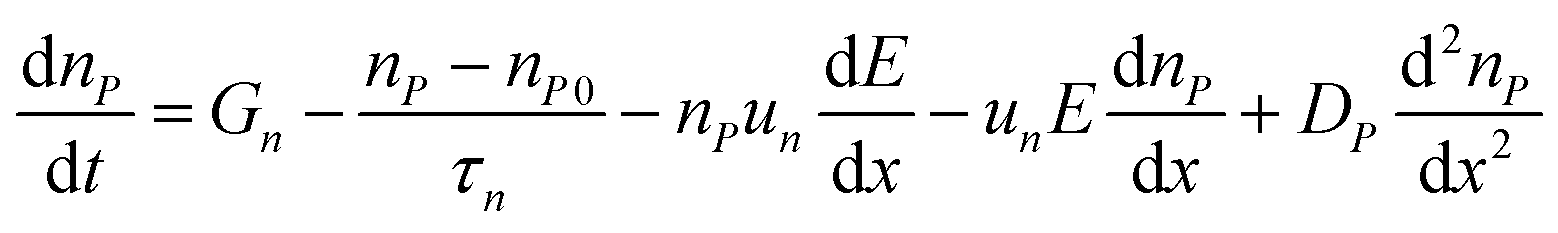
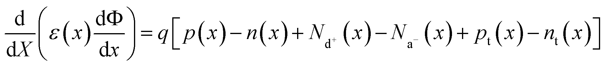

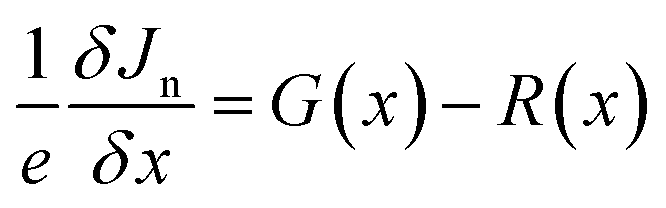
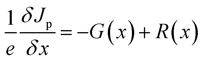

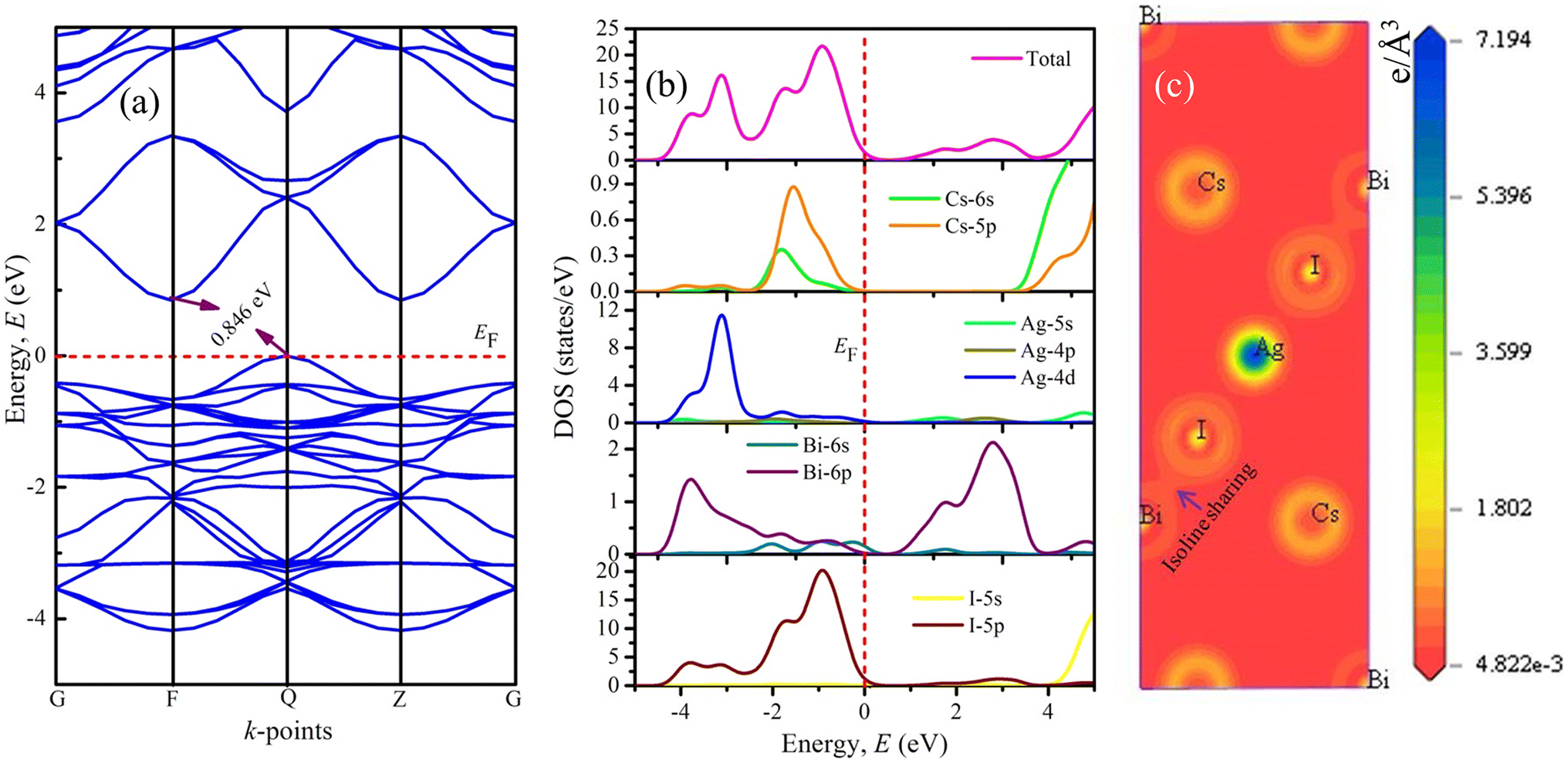
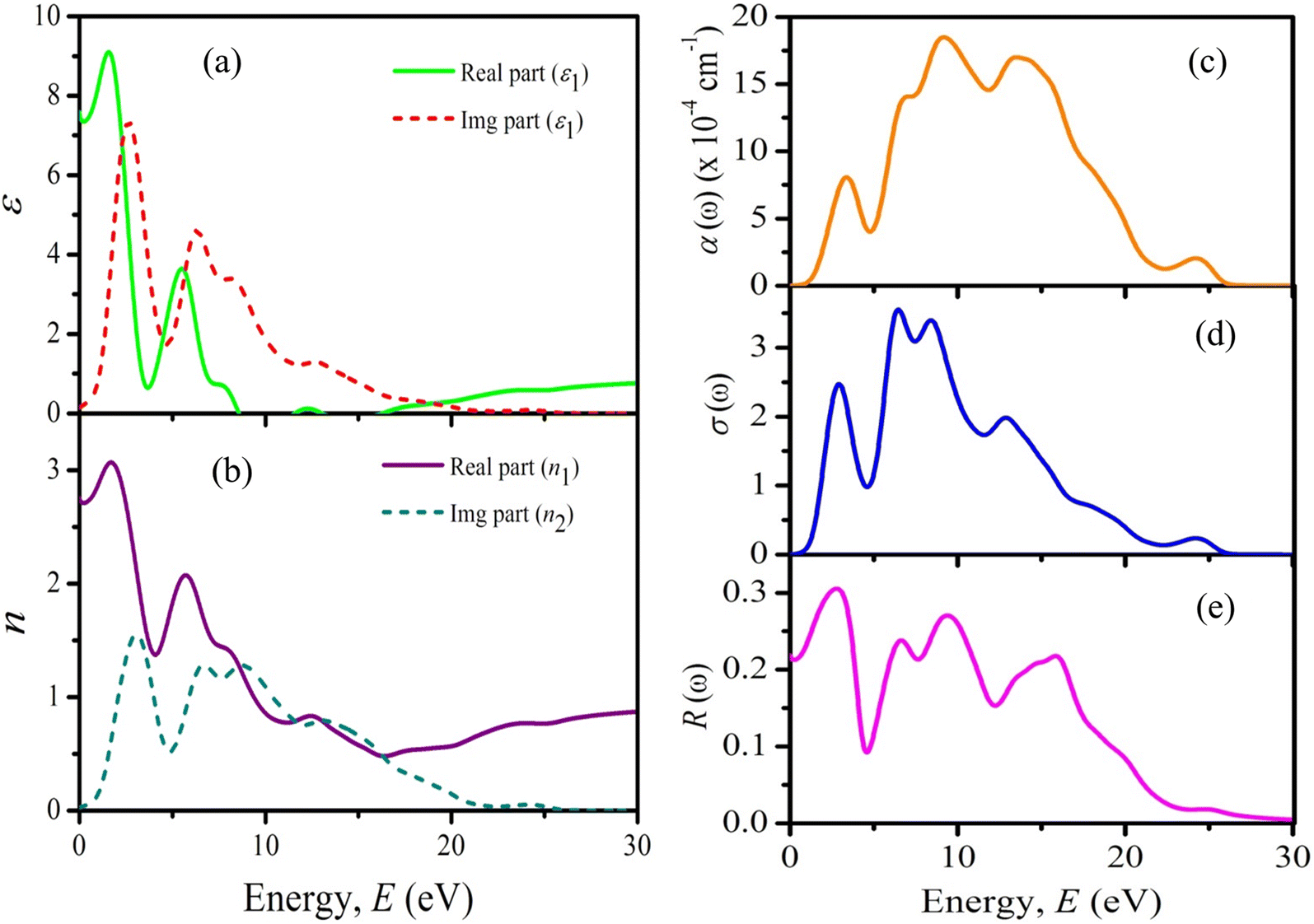
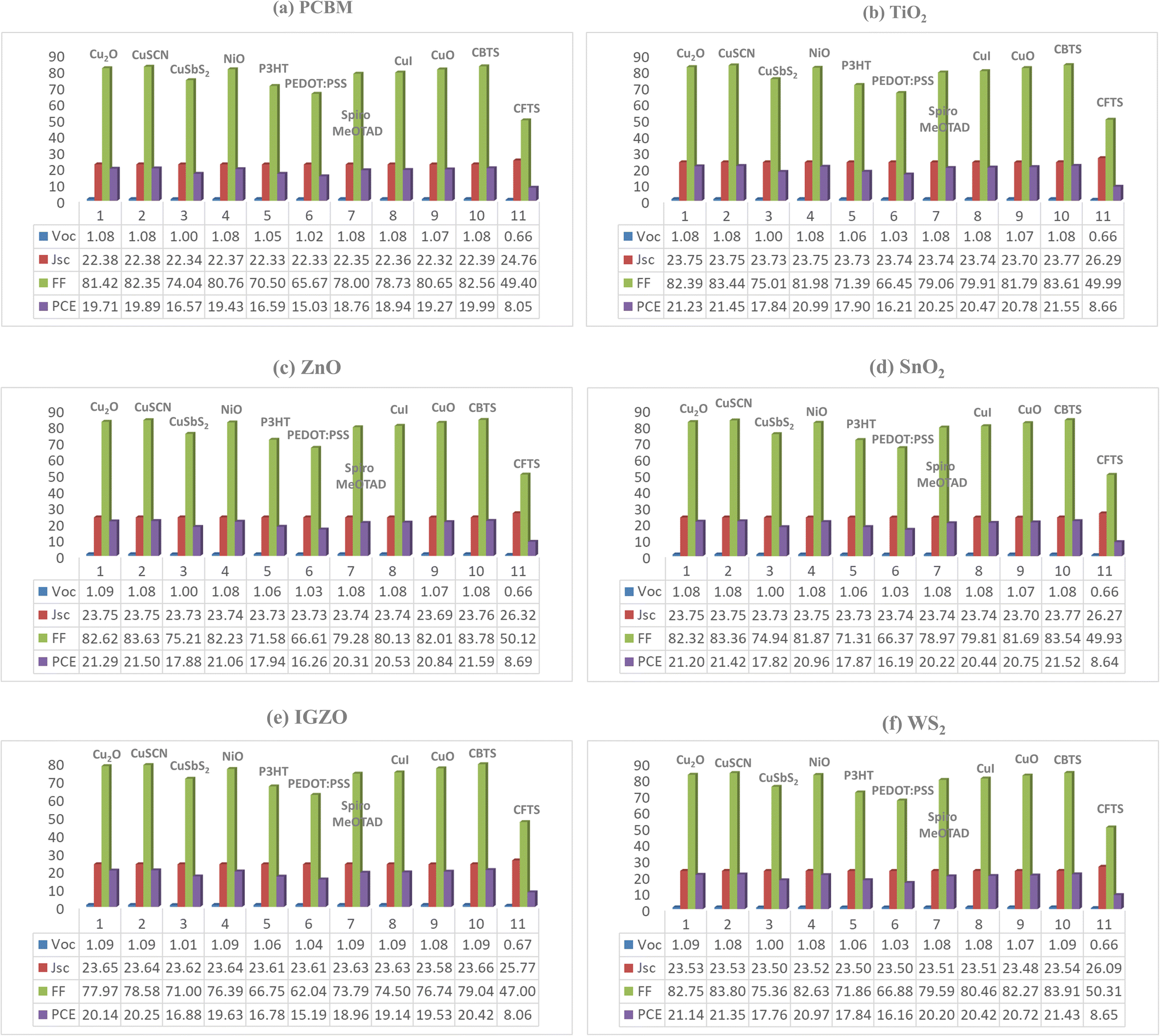
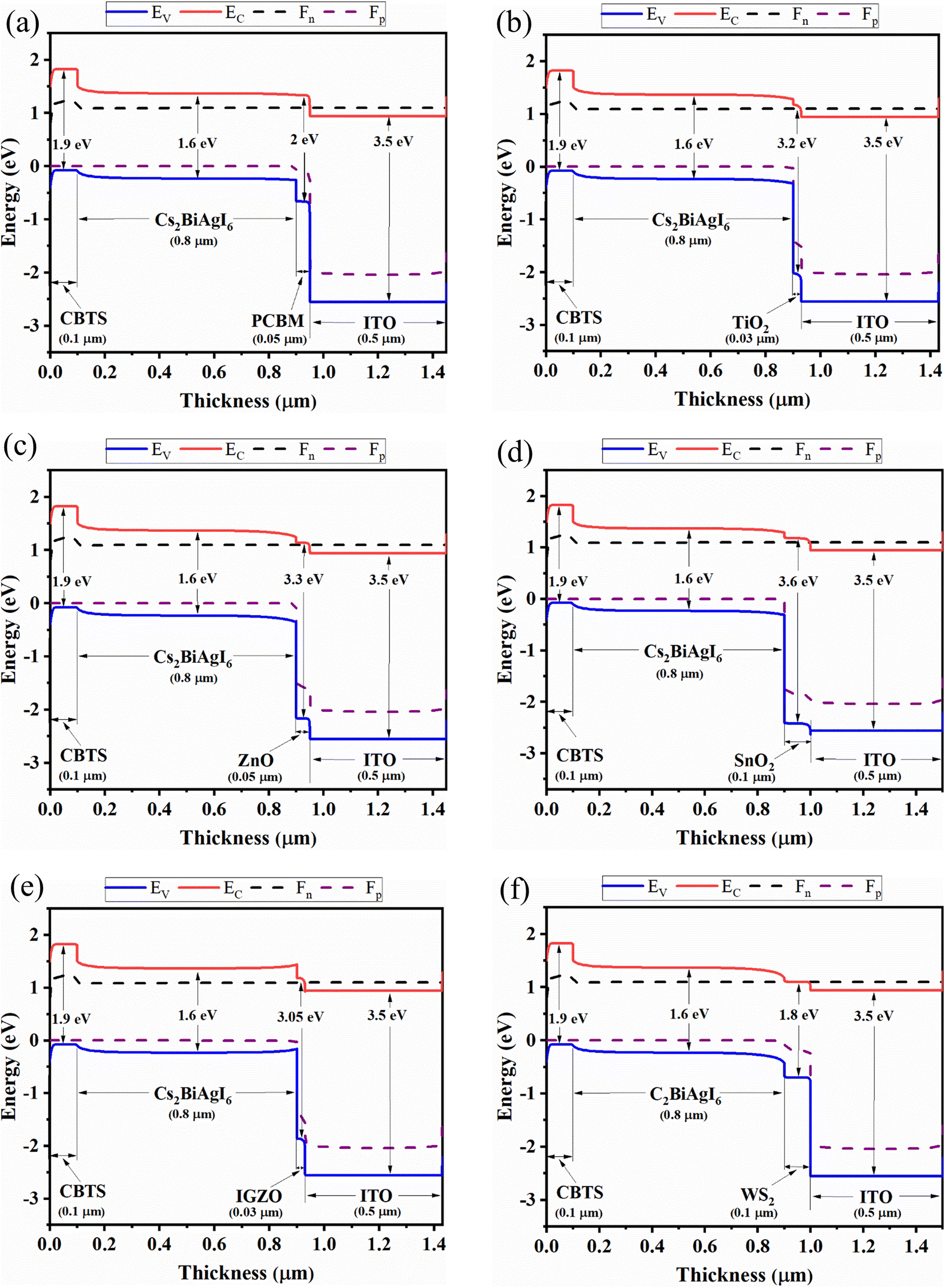
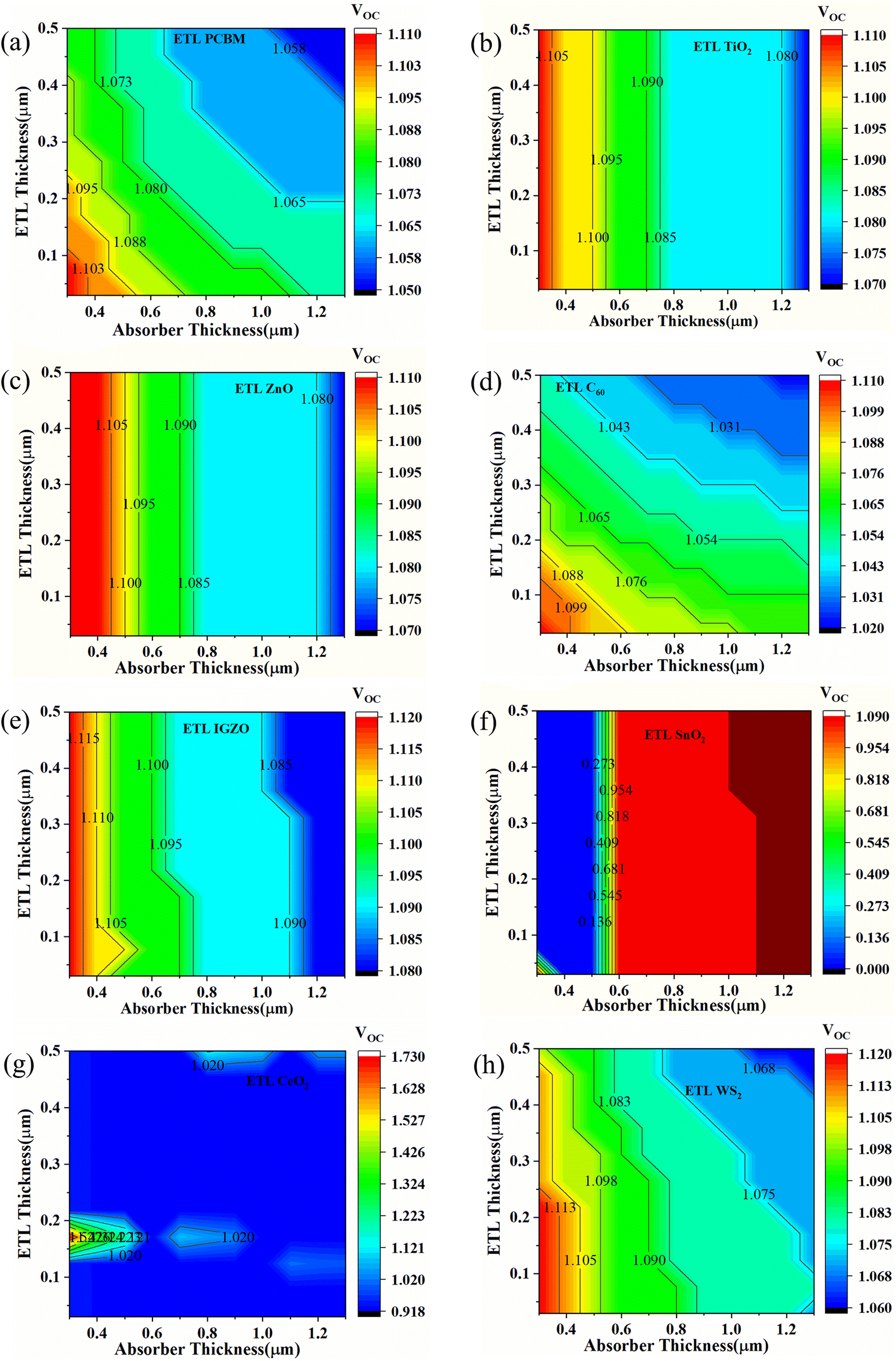

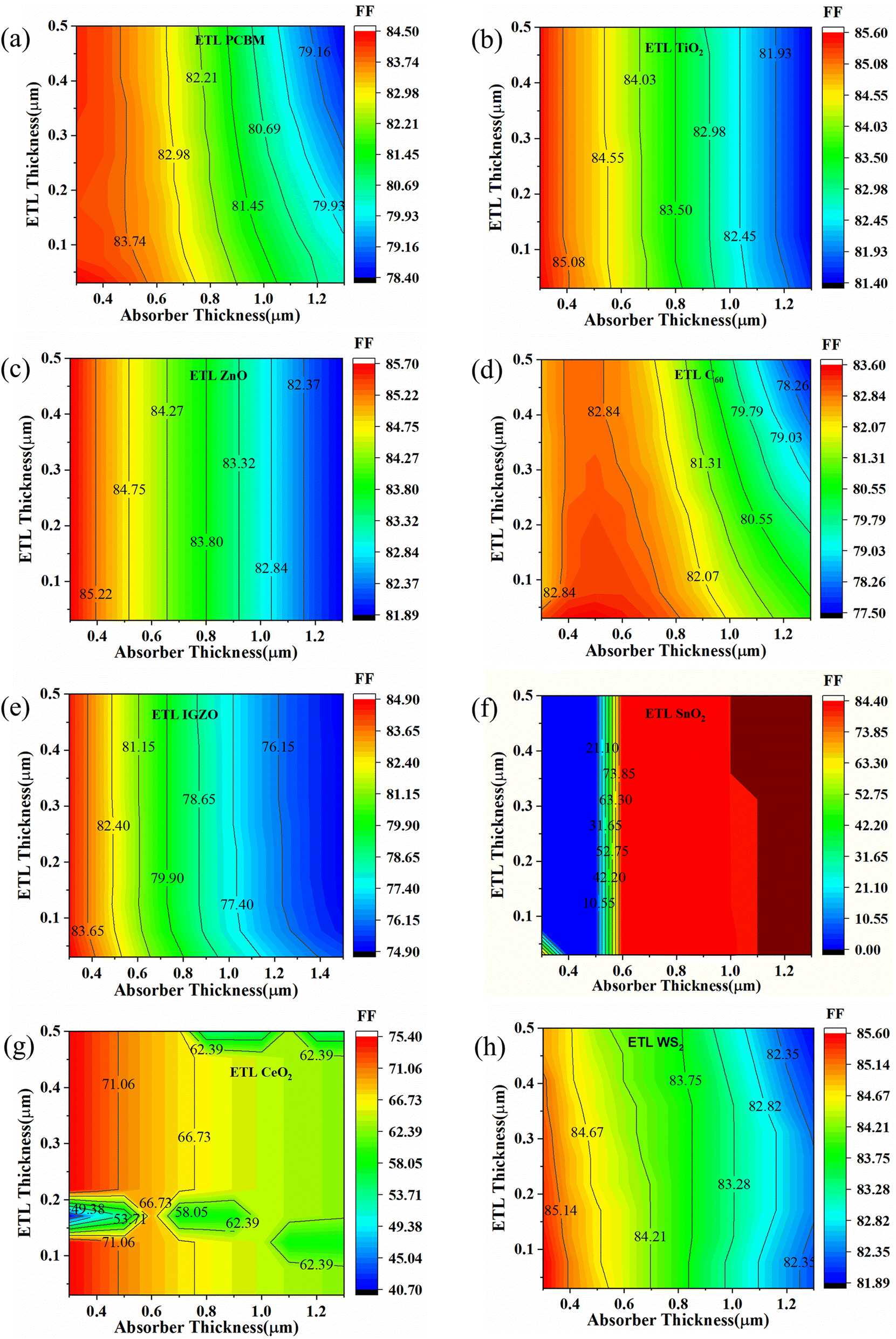
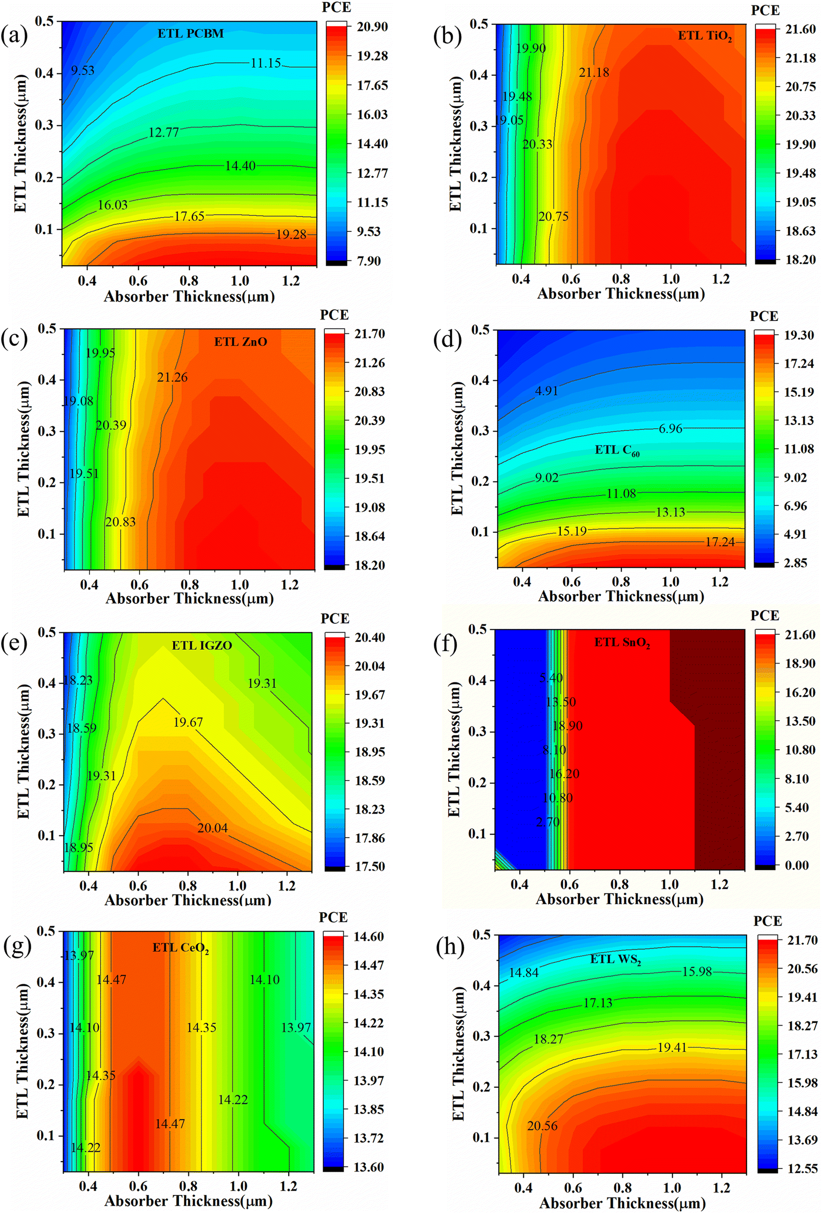
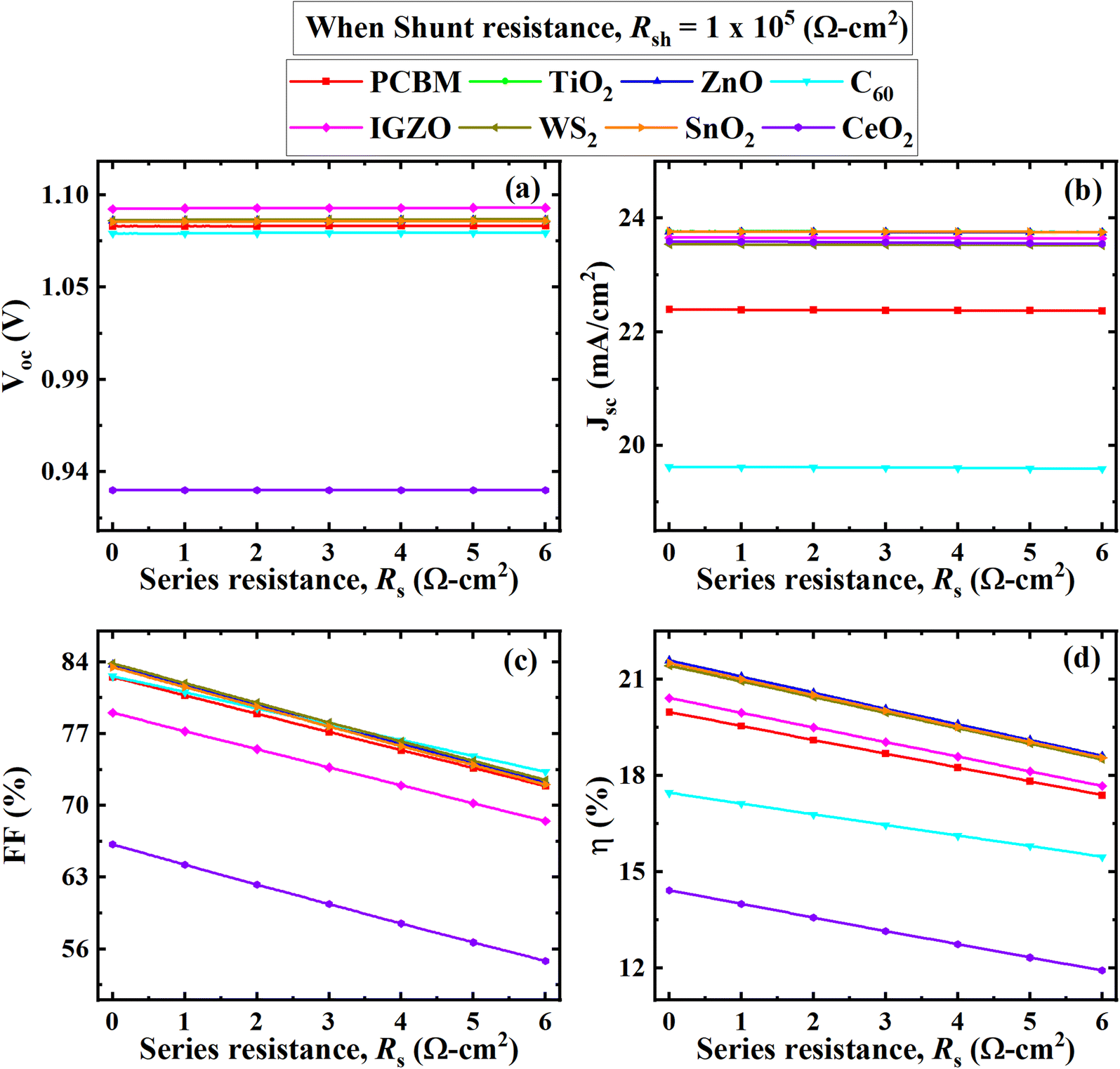
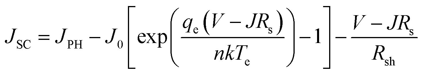
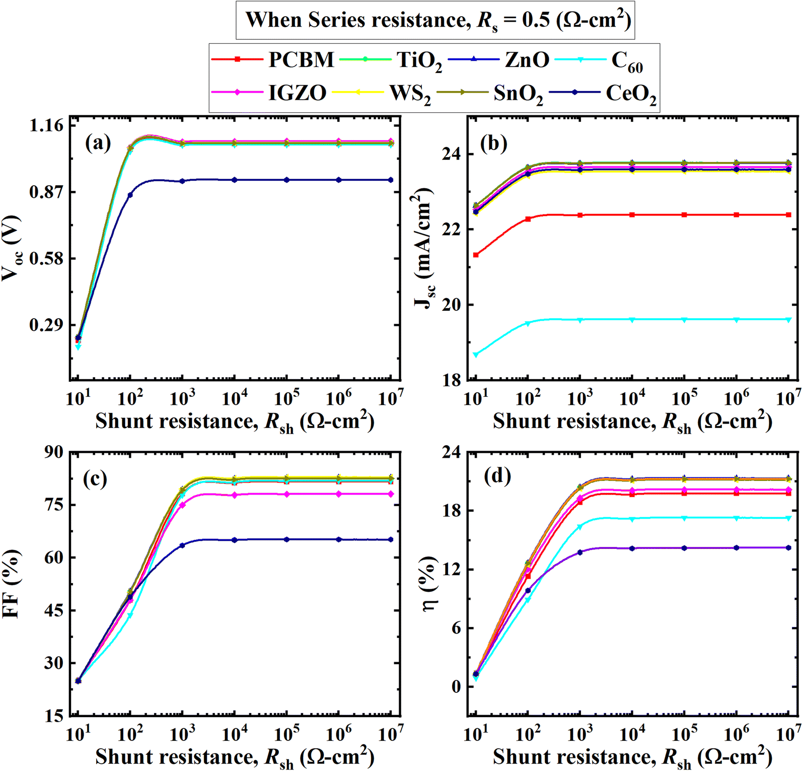

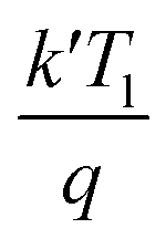 stands for the thermal voltage, and A stands for the ideality factor.