DOI:
10.1039/D2RA06139B
(Paper)
RSC Adv., 2022,
12, 30322-30327
Anisotropic dependence of radiation from excitons in Ga2O3/MoS2 heterostructure†
Received
29th September 2022
, Accepted 17th October 2022
First published on 24th October 2022
Abstract
The anisotropic dependence of radiation arising from exciton recombination in the Ga2O3/MoS2 heterostructure is investigated, using density functional theory and the Bethe–Salpeter equation. The wurtzite (WZ) and zinc blende (ZB) structures of the Ga2O3 monolayer with ferroelectric (FE) properties are assembled with a MoS2 monolayer. Projected band structure, charge transfer and life time of excitons are discussed, to analyze which transition may be important to the creation of excitons from the electron–hole pair. A general formula of the angle-dependent intensities of radiation is derived. The characteristics of angle-dependent intensities that are closely related to the dipole moment of excitons are discussed, from the viewpoint of in-plane and out-of-plane polarizations. These predictions on radiation of the Ga2O3/MoS2 heterostructure should guide exciton dynamics in low dimensional systems and rational design of optoelectronic devices.
1 Introduction
The applications of deep-ultraviolet photodetectors have made great progress in recent years. As one of the ultra-wide band gap (4.6–4.9 eV)1,2 materials, gallium oxide (Ga2O3) has very unique electronic and optical properties, which make it suitable to be the building blocks of solar-blind photodetectors3–6 and power devices.7,8 According to different crystal structures, it can be classified as five different polymorphs (α, β, γ, δ, ε).9–11
Among them, the stable β-Ga2O3 based semiconductor materials, are suitable for applications in next-generation power electronic and optoelectronic devices. It is reported that Schottky interfaces based on β-Ga2O3 can realize a large Schottky barrier height, which makes high-temperature operation possible.12 A vertical-type Schottky photodetector based on a (100)-oriented β-Ga2O3 substrate has been fabricated with simple processes of thermal annealing and vacuum evaporation.13 Optoelectronic analysis reveals that the heterojunction device is virtually blind to light illumination with wavelength longer than 280 nm, assembled by coating multilayer graphene on β-Ga2O3 wafer.14 Self-powered solar-blind photodetectors based on diamond/β-Ga2O3 heterojunctions have been fabricated successfully. These photodetectors can exhibit repeatability and stability without any external power supply.15 What's more, a deep UV photodiode is fabricated using a heterojunction between β-Ga2O3 and GaN. The response time of the photodiode is in the order of sub-milliseconds.16
Besides the bulk β-Ga2O3, with the rapidly growing synthesis technology in recent years, as one of the building blocks of functional devices, the two-dimensional (2D) van der Waals materials have been regarded as a promising material for the breathtaking through of nanotechnology and its applications. β-Ga2O3 films are grown on SrTiO3 (100) substrate by a high-vacuum MOCVD system.17 As the similar way in graphene, mechanical exfoliation of the bulk β-Ga2O3 by using an adhesive tape is followed by plasma etching to tune its thickness.18 Feng et al. report the successful fabrication of 2D Ga2O3 from the corresponding GaSe nanosheets and a solar blind photodetector based on 2D Ga2O3. The as-prepared 2D β-Ga2O3 is polycrystalline and has a thickness of less than 10 nm.19 As its unusual asymmetrical structure of 2D Ga2O3, by using selected surface orientations, improving the selectivity and sensitivity of gas sensors and release controlled by a ferroelectric switch become possible.20–22 Meng et al. predict a stable hexagonal phase of 2D Ga2O3 and In2O3, by using a global searching method based on an evolutionary algorithm, combined with density functional theory (DFT) simulations.23
The devices based on van der Waals heterostructures widely broaden the applications of these 2D ferroelectric materials. E.g. high breakdown electric field in β-Ga2O3/graphene vertical barrister heterostructure.,24 Ga2O3/GaN heterostructural ultraviolet photodetectors,25 deep-ultraviolet photodetection using single-crystalline β-Ga2O3/NiO heterojunctions,26 ultrahigh deep-UV sensitivity in graphene-gated β-Ga2O3 phototransistors,3 and PdCoO2/β-Ga2O3 Schottky diodes for high-temperature operation.12
Another emerging 2D semiconductors with a sizable direct bandgap and novel physical properties are monolayer group VI transition metal dichalcogenides (TMDs).27–30 Both theoretically and experimentally, light emitting devices based on TMDs have been demonstrated low threshold.29 WSe2, WS2, MoSe2 and MoS2 monolayers can be flexibly exfoliated onto the same SiO2/Si substrate,31 which makes it suitable to be the building blocks of heterostructures.
Based on In2Se3 and other III2–VI3 van der Waals materials, using first-principles calculations, Ding et al. discover a branch of the 2D materials family, which exhibits room-temperature ferroelectricity (FE) with reversible spontaneous electric polarization in both out-of-plane and in-plane orientations.32 In addition, a novel 2D Ga2O3 monolayer is constructed and systematically investigated by first-principles calculations. The 2D Ga2O3 monolayer has an asymmetric configuration with a quintuple-layer (QL) atomic structure, the same as the well-studied α-In2Se3,32 and is expected to be experimentally synthesized.33 What's more, the mismatch of crystal lattice between Ga2O3 and MoS2 monolayer is less than 3%.32,34,35
In material engineering, one of the difficult task is combining the best of different ingredients into one ultimate device. Thereby, in this study, we propose a model of Ga2O3/MoS2 heterostructure, using DFT and Bethe–Salpeter equation.36–38 The wurtzite (WZ) and zinc blende (ZB) structures of Ga2O3 monolayer with ferroelectric (FE) properties are assembled with MoS2 monolayer. The projected band structure and charge transfer are discussed, and explain the life time of radiation from exciton recombination. The angle-dependent intensities of radiation are derived, which is general and can be applied to other similar systems. Finally, the characteristics of angle-dependent intensities including in-plane and out-of-plane polarization, are presented, which can be measured in future experiments.
2 Methods
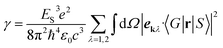
According to the Fermi's golden rule, the transition from excited state |S〉 to ground state |G〉, arising from the electron–photon interaction Hint can be written as,| |
 | (1) |
where γ represents the rate of emission of a photon with angular frequency ωk, and ES is the exciton energy. The Hamiltonian describing the electron–photon interaction can be expressed as,39| |
 | (2) |
where p is the electron momentum operator and the vector-potential operator A(r) is,40| |
 | (3) |
where  and âkλ denote the creation and annihilation operators for a phonon of with momentum k and vibrating direction eλ. With the relation between operators r and p (p = −im/ℏ[r, H]), inserting eqn (3) into (2), the rate in eqn (1) can be written as,
| |
 | (4) |
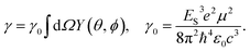
In general, the unit vector of light propagating direction can be set as ek = (sin![[thin space (1/6-em)]](https://www.rsc.org/images/entities/char_2009.gif) θcosϕ, sinθsinϕ, cosθ). As the intensity of emitting light with a given angle is proportional to the rate of radiation, eqn (5) can provide angle-dependent polar plots of the photoluminescence (PL) spectroscopy in experiments. Furthermore, the contributions of intensity can be measured experimentally in in-plane (IP) and out-of-plane (OP) directions, respectively, as shown in eqn (6). The rate γ of radiation can be expressed as,
θcosϕ, sinθsinϕ, cosθ). As the intensity of emitting light with a given angle is proportional to the rate of radiation, eqn (5) can provide angle-dependent polar plots of the photoluminescence (PL) spectroscopy in experiments. Furthermore, the contributions of intensity can be measured experimentally in in-plane (IP) and out-of-plane (OP) directions, respectively, as shown in eqn (6). The rate γ of radiation can be expressed as,
| |
 | (5) |
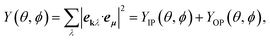
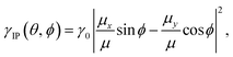
Here, 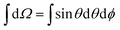 is the integral over solid angle. γ0 is the rate constant independent of radiation angles, with μ = 〈G|r|S〉. And the angle-dependent function Y(θ, ϕ) is denoted as,
| |
 | (6) |
with the unit vector of in-plane polarization
eIP = (sin
ϕ, −cos
ϕ, 0) and the unit vector of out-of-plane polarization
eOP = (cos
θcos
ϕ, cos
θsin
ϕ, −sin
θ).
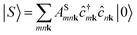
Finally, the difficulty is to evaluate |〈G|r|S〉|, which is closely related to the dipole moment of exciton. Based on the expansion coefficient ASmnk by solving the Bethe–Salpeter equation (BSE), implemented in the BerkeleyGW codes,36–38 the wave function of an exciton is expressed as a linear combinations of electron–hole transitions,
| |
 | (7) |
where

and
ĉnk denote the creation and annihilation operators for an electron in the
n-th electronic state with momentum
k. The indices
m and
n run over all the conduction and valence bands, respectively. Overall, with the exciton wave function, the dipole moment of exciton can be obtained. The detail derivatives of the above equations can be found in the ESI.
†
3 Results and discussions
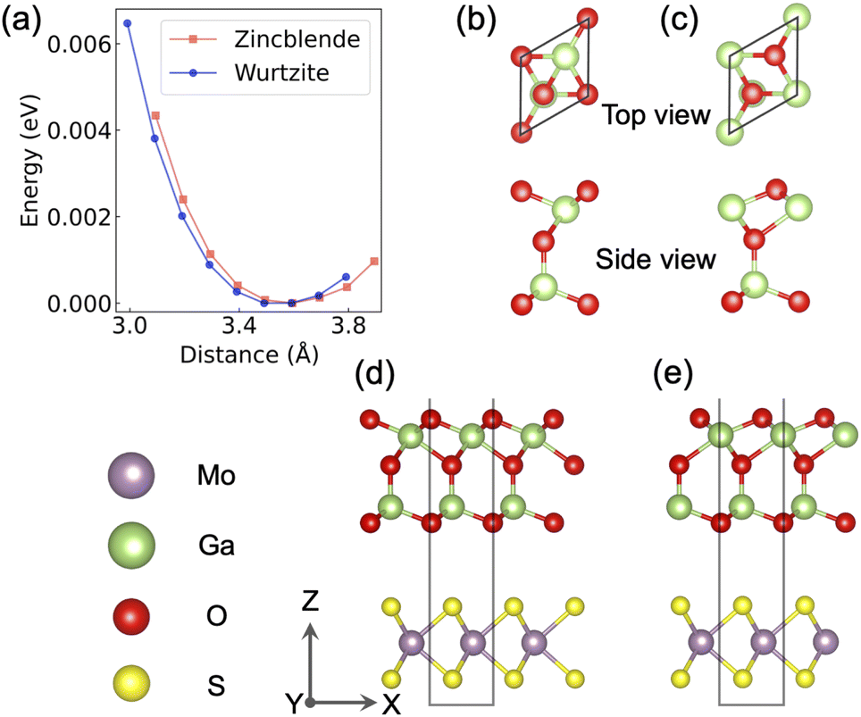
In this study, two kinds of Ga2O3 monolayers with ferroelectric (FE-WZ and FE-BZ) phases are included. As shown in Fig. 1b and c, these two structures with five-atomic-layers QL stacking, are demonstrated stable in In2Se3.32 In addition, it is necessary to considering the conventional ‘lattice mismatch’ issue, when constructing vertical heterostructures using different 2D materials. The optimized lattice parameters of FE-ZB Ga2O3 are a = 3.08 Å with GGA-PBE.33 For the bulk MoS2, the lattice parameter is a = 3.16 Å,41,42 which means that the mismatch rate of MoS2 and Ga2O3 monolayers should be less than 3%. The energy-distance (between MoS2 and Ga2O3 monolayer) curve is also plotted in Fig. 1a. In our calculations, the distance for the relaxed FE-ZB/MoS2 (Fig. 1d) and FE-WZ/MoS2 (Fig. 1e) heterostructures are 3.58 Å and 3.51 Å, respectively.
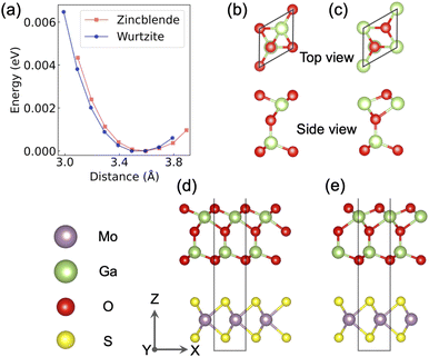 |
| | Fig. 1 (a) Energy-distance (between MoS2 and Ga2O3 monolayer) curve for FE-ZB/MoS2 and FE-WZ/MoS2 heterostructure, marked with red and blue point line, respectively. Top and side view crystal structure of FE-ZB (b) and FE-WZ (c) Ga2O3 monolayer. Side view of FE-ZB/MoS2 (d) and FE-WZ/MoS2 (e) heterostructure. The red, green, violet and yellow balls denote O, Ga, Mo and S atoms, respectively. | |
3.1 Electronic structures and crystal stability
Before the investigations of excited states, it is necessary to understand the electronic structures from the viewpoint of DFT. To better study the electronic structure of Ga2O3/MoS2 heterostructures, the atom-projected band structures and partial density of states (PDOS) for both FE-ZB/MoS2 and FE-WZ/MoS2 heterostructures are exhibited in Fig. 2. As reported in previous literature, both FE-ZB and FE-WZ Ga2O3 monolayers have indirect band gaps. For the FE-ZB/MoS2 heterostructure, it is still an indirect-band-gap semiconductor, the minimum of conduction band (CBM) locates at Γ point, while the maximum of valence band (VBM) locates at K point. In the FE-WB/MoS2 heterostructure, both CBM and VBM locate at K point, which make it a direct-band-gap semiconductor with smaller gaps. We notice that, in the Ga2O3/MoS2 heterostructure, the predominant contribution of the conduction band comes from Mo atoms of MoS2, while for the valence band, the oxygen atoms of Ga2O3 make the main contribution. This point can also be verified by the corresponding PDOS in the right panel of Fig. 2. This means that, in this Ga2O3/MoS2 heterostructures, it seems that, the electron should lie in the conduction band of MoS2, while the hole should come from the valence band in Ga2O3. To verify the stability of the heterostructure, the phonon band structures are presented in Fig. 3. We notice that there are totally 24 phonon branches, as there are 8 atoms in the unit cell. In the plot of phonon band, the absence of imaginary phonon modes indicates that, the crystal structure of the heterostructure of FE-ZB/MoS2 and FE-WZ/MoS2 heterostructures could be dynamically stable.
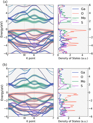 |
| | Fig. 2 Band structure and PDOS of (a) FE-ZB/MoS2 and (b) FE-WZ/MoS2 heterostructures. The maximum of valence band (VBM) is set at zero. Atom-projected band structures and PDOS are highlighted with red, green, violet and yellow colors for O, Ga, Mo and S elements, respectively. | |
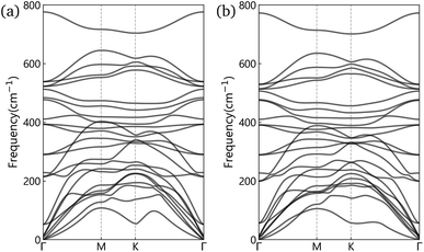 |
| | Fig. 3 Phonon band structure of (a) FE-ZB/MoS2 and (b) FE-WZ/MoS2 heterostructures. | |
3.2 Charge transfer and life time
As is known to all, the formation of exciton is closely related to the electron–hole pairs, which can be reflected by the distribution of charge density in the heterostructure and its interface. The charge density difference Δρ is defined as:| | |
Δρ = ρall − ρGa2O3 − ρMoS2
| (8) |
where ρall represents the charge density of the G2O3/MoS2 heterostructure, while ρGa2O3 and ρMoS2 denote the charge density of G2O3 and MoS2 monolayers, respectively. From the side view of charge density difference in Fig. 4, the charge transfer mainly happens in MoS2 monolayer. The charge moves from the outside part of MoS2, and accumulates in the interface, near the inside part of MoS2. Compared with MoS2, the charge density difference of G2O3 monolayer changes very little, and mainly happens on the lowest oxygen layer, close to the interface.
 |
| | Fig. 4 Side view of calculated charge density difference of (a) FE-ZB/MoS2 and (b) FE-WZ/MoS2 heterostructures. The yellow and cyan colors represent charge accumulation and loss, respectively. | |
As a supplement to the charge density difference, the exciton wave functions are provided. Taking the Tamm–Dancoff approximation by considering only valence to conduction band transitions, the wave function in real space can be expressed as:38
| |
 | (9) |
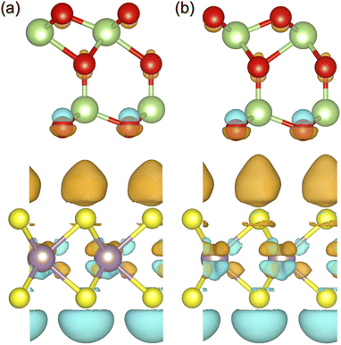
Here, re and rh denote the position of electron and hole in an electron–hole pair. As shown in Fig. 5, the wave function of exciton mainly locates on the Ga2O3 monolayer, in both the lowest-energy S1 and second-lowest S2 exciton states. This point is demonstrated by the charge density difference Δρ, which happens mostly in the same monolayer of the heterostructure, rather than interlayer. Compared with the flat and spreading status of S1, the wave function of S2 appears much more localized, with two accumulation center in the supercell of 10 × 10.
 |
| | Fig. 5 Top and side view of calculated exciton wave functions of FE-ZB/MoS2 heterostructures for the lowest-energy S1 (a) and second-lowest S2 (b) exciton states. The position of hole is fixed in the center of MoS2 monolayer of the heterostructure. The wave function is visualized in a supercell of 10 × 10. | |
The radiative life time (1/γ) of the lowest S1 and second S2 lowest-energy excited states for FE-ZB/MoS2 and FE-WZ/MoS2 heterostructures are summarized in Table 1. The radiation of exciton is closely related to the lower-energy bright states. In our Ga2O3/MoS2 heterostructure, the S1 is nondegenerate, while S2 and S3 are doubly degenerate. As comparison, the lowest-energy exciton states (S1 and S2) of Ga2O3 monolayer are doubly degenerate (for FE-ZB Ga2O3 monolayer ES1 = ES2 = 3.15 eV, for FE-WZ Ga2O3 monolayer ES1 = ES2 = 3.38 eV), which is related to the two equivalent K and K′ points in the reciprocal lattice. Compared with the large exciton energy (more than 3.0 eV) in Ga2O3 monolayer, the energy of S1 in the heterostructure is about 1.2–1.3 eV. And as the doubly degenerate property and larger exciton energy, the life time of S2 (∼90 ns) is much shorter than that of S1 (∼500 ns) in both FE-ZB/MoS2 and FE-WZ/MoS2 heterostructures. In spite that our calculation can not give exact quantitative results, it still can provide qualitative guidance in future experiments.
Table 1 The radiative lifetime (1/γ) of FE-ZB/MoS2 and FE-WZ/MoS2 heterostructures
| System |
ES (eV) |
Lifetime (ns) |
| FE-ZB/MoS2 |
S1 (1.27) |
554 |
| FE-ZB/MoS2 |
S2 (2.00) |
93 |
| FE-WZ/MoS2 |
S1 (1.23) |
519 |
| FE-WZ/MoS2 |
S2 (1.95) |
90 |
3.3 Angle dependence of radiation
To further understand the anisotropic radiation of exciton, the angle-dependent intensity is investigated, the results of which can be compared with that in experiments. In a polar coordinate system, the propagating direction of light with k vector can be written as, ek = (sinθcosϕ, sinθsinϕ, cosθ), with polar angle θ and azimuth angle ϕ. As shown in Fig. 1, the x and y axes are on the plane of MoS2 and G2O3 monolayers. The polarization direction ekλ of the light can be expressed as the in-plane (IP) and out-of-plane (OP) unit vectors, with eIP = (sinϕ, −cosϕ, 0), and eOP = (cosθcosϕ, cosθsinϕ, −sinθ). In general, the contribution from IP and OP polarizations can be written as:| |
 | (10) |
| |
 | (11) |
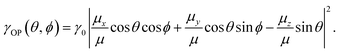
Fig. 6 shows the polar plots of the angle-dependent intensities for radiation of the lowest-energy exciton, with specific polar angle (θ = 0, 45, 135° for FE-ZB/MoS2 and FE-WZ/MoS2 heterostructure, respectively. We notice that, for the intensity of IP polarization, it does not depend on the polar angle θ, only the function of azimuth angle ϕ. Both IP and OP intensities have two maxima, the connecting line of which are perpendicular to each other. When θ = 0°, the total intensity is isotropic, which means that the two contributions from IP and OP are equal. As shown in eqn (11), when the polar angle θ = 0°, there is no contribution from z direction, which means that the OP polarization lies on the x–y plane, as the IP polarization dose. When the polar angle θ = 45° (Fig. 6c and d), for the OP polarization, the intensity of one maximum is much larger than another one. Thus, the total intensity is anisotropic, obviously depending on the azimuth angle ϕ. When the polar angle θ = 135° (Fig. 6e and f), the configuration of radiation is similar, but the position of maxima just simply reversed. For FE-ZB/MoS2 and FE-WZ/MoS2 heterostructures, their configuration of radiation are similar, and the main difference comes from the locations of maxima. From eqn (10) and (11), we notice that, the maxima of intensities depend on the dipole moment vector, which can be demonstrated by experiments. In other words, the radiation of IP and OP polarizations can be measured in experiments. With these configurations of radiation, the dipole moment of exciton can be measured indirectly.
 |
| | Fig. 6 Polar plots of the angle-dependent intensities for radiation of the lowest-energy exciton (S1), with specific polar angle θ [for (a and b), θ = 0°, for (c and d), θ = 45°, for (e and f), θ = 135°]. The left (a, c and e) and right (b, d and f) panels are for FE-ZB/MoS2 and FE-WZ/MoS2 heterostructures, respectively. The maximum scale range of the intensities in the polar plots is 2 × 10⁻³ ns−1. | |
4 Conclusions
We have investigated the anisotropic dependence of radiation arising from exciton recombination in Ga2O3/MoS2 heterostructure, using density functional theory and Bethe–Salpeter equation. The FE-ZB and FE-WZ structures of Ga2O3 monolayer with ferroelectric properties are assembled with MoS2 monolayer. From the projected band structure, we find that the predominant contribution of the conduction band comes from Mo atoms of MoS2, while for the valence band, the oxygen atoms of Ga2O3 make the main contribution. The charge transfer and wave function of exciton reveal that, the charge density difference happens mainly in the same monolayer of the heterostructure. The life time of doubly degenerate S2 (∼90 ns) is much shorter than that of S1 (∼500 ns) in both FE-ZB/MoS2 and FE-WZ/MoS2 heterostructures. The characteristics of angle-dependent intensities are discussed. We find that, the maxima of intensity depend on the dipole moment vector, which can be demonstrated by experiments. These predictions on radiation of Ga2O3/MoS2 heterostructure should guide rational design of optoelectronic devices in low dimensional systems.
Conflicts of interest
There are no conflicts of interest to declare.
Acknowledgements
This work was supported by the Guangxi Natural Science Foundation (Grant No. 2021GXNSFAA220129), the Project of Improving the Basic Scientific Research Ability of Young and Middle-aged Teachers in Universities of Guangxi (Grant No. 2022KY0784), the Foundation of Guilin University of Aerospace Technology (Grant No. 2021BJXM019), the High-Performance Servers of Guilin University of Aerospace Technology.
Notes and references
- S. Stepanov, V. Nikolaev, V. Bougrov and A. Romanov, Rev. Adv. Mater. Sci., 2016, 44, 63–86 CAS.
- K. A. Mengle, G. Shi, D. Bayerl and E. Kioupakis, Appl. Phys. Lett., 2016, 109, 212104 CrossRef.
- S. Kim, S. Oh and J. Kim, ACS Photonics, 2019, 6, 1026–1032 CrossRef CAS.
- S. Pearton, J. Yang, P. H. Cary IV, F. Ren, J. Kim, M. J. Tadjer and M. A. Mastro, Appl. Phys. Rev., 2018, 5, 011301 Search PubMed.
- H. Chen, K. Liu, L. Hu, A. A. Al-Ghamdi and X. Fang, Mater. Today, 2015, 18, 493–502 CrossRef CAS.
- L. Sang, M. Liao and M. Sumiya, Sensors, 2013, 13, 10482–10518 CrossRef CAS.
- K. Arora, N. Goel, M. Kumar and M. Kumar, ACS Photonics, 2018, 5, 2391–2401 CrossRef CAS.
- W. Guo, Y. Guo, H. Dong and X. Zhou, Phys. Chem. Chem. Phys., 2015, 17, 5817–5825 RSC.
- D. Kaur and M. Kumar, Adv. Opt. Mater., 2021, 9, 2002160 CrossRef CAS.
- J. Zhang, J. Shi, D.-C. Qi, L. Chen and K. H. Zhang, APL Mater., 2020, 8, 020906 CrossRef CAS.
- T. Gake, Y. Kumagai and F. Oba, Phys. Rev. Mater., 2019, 3, 044603 CrossRef CAS.
- T. Harada, S. Ito and A. Tsukazaki, Sci. Adv., 2019, 5, eaax5733 CrossRef CAS.
- T. Oshima, T. Okuno, N. Arai, N. Suzuki, S. Ohira and S. Fujita, Appl. Phys. Express, 2008, 1, 011202 CrossRef.
- W.-Y. Kong, G.-A. Wu, K.-Y. Wang, T.-F. Zhang, Y.-F. Zou, D.-D. Wang and L.-B. Luo, Adv. Mater., 2016, 28, 10725–10731 CrossRef CAS PubMed.
- Y.-C. Chen, Y.-J. Lu, C.-N. Lin, Y.-Z. Tian, C.-J. Gao, L. Dong and C.-X. Shan, J. Mater. Chem. C, 2018, 6, 5727–5732 RSC.
- S. Nakagomi, T.-a. Sato, Y. Takahashi and Y. Kokubun, Sens. Actuators, A, 2015, 232, 208–213 CrossRef CAS.
- D. Wang, X. Ma, H. Xiao, R. Chen, Y. Le, C. Luan, B. Zhang and J. Ma, Mater. Res. Bull., 2021, 111718 Search PubMed.
- Y. Kwon, G. Lee, S. Oh, J. Kim, S. J. Pearton and F. Ren, Appl. Phys. Lett., 2017, 110, 131901 CrossRef.
- W. Feng, X. Wang, J. Zhang, L. Wang, W. Zheng, P. Hu, W. Cao and B. Yang, J. Mater. Chem. C, 2014, 2, 3254–3259 RSC.
- J. Zhao, X. Huang, Y. Yin, Y. Liao, H. Mo, Q. Qian, Y. Guo, X. Chen, Z. Zhang and M. Hua, J. Phys. Chem. Lett., 2021, 12, 5813–5820 CrossRef CAS PubMed.
- C. Jin, X. Tang, X. Tan, S. C. Smith, Y. Dai and L. Kou, J. Mater. Chem. A, 2019, 7, 1099–1106 RSC.
- X. Tang, J. Shang, Y. Gu, A. Du and L. Kou, J. Mater. Chem. A, 2020, 8, 7331–7338 RSC.
- R. Meng, M. Houssa, K. Iordanidou, G. Pourtois, V. Afanasiev and A. Stesmans, J. Appl. Phys., 2020, 128, 034304 CrossRef CAS.
- X. Yan, I. S. Esqueda, J. Ma, J. Tice and H. Wang, Appl. Phys. Lett., 2018, 112, 032101 CrossRef.
- R. Tang, G. Li, Y. Jiang, N. Gao, J. Li, C. Li, K. Huang, J. Kang, T. Wang and R. Zhang, ACS Appl. Electron. Mater., 2021, 4, 188–196 CrossRef.
- K.-H. Li, N. Alfaraj, C. H. Kang, L. Braic, M. N. Hedhili, Z. Guo, T. K. Ng and B. S. Ooi, ACS Appl. Mater. Interfaces, 2019, 11, 35095–35104 CrossRef CAS PubMed.
- K. F. Mak, C. Lee, J. Hone, J. Shan and T. F. Heinz, Phys. Rev. Lett., 2010, 105, 136805 CrossRef PubMed.
- Q. H. Wang, K. Kalantar-Zadeh, A. Kis, J. N. Coleman and M. S. Strano, Nat. Nanotechnol., 2012, 7, 699–712 CrossRef CAS PubMed.
- X. Meng, R. R. Grote, W. Jin, J. I. Dadap, N. C. Panoiu and R. M. Osgood, Opt. Lett., 2016, 41, 2636–2639 CrossRef CAS.
- K. Novoselov, o. A. Mishchenko, o. A. Carvalho and A. Castro Neto, Science, 2016, 353, aac9439 CrossRef CAS.
- J. Jadczak, J. Kutrowska-Girzycka, P. Kapuściński, Y. Huang, A. Wójs and z. Bryja, Nanotechnology, 2017, 28, 395702 CrossRef CAS PubMed.
- W. Ding, J. Zhu, Z. Wang, Y. Gao, D. Xiao, Y. Gu, Z. Zhang and W. Zhu, Nat. Commun., 2017, 8, 1–8 CrossRef CAS PubMed.
- Y. Liao, Z. Zhang, Z. Gao, Q. Qian and M. Hua, ACS Appl. Mater. Interfaces, 2020, 12, 30659–30669 CrossRef CAS.
- J. Yu, C. Xia, Z. Hu, X. Hao, L. Wang and Q. Fang, et al., Phys. Chem. Chem. Phys., 2022, 24, 3289–3295 RSC.
- C. Adessi, S. Pecorario, S. Thebaud and G. Bouzerar, Phys. Chem. Chem. Phys., 2020, 22, 15048–15057 RSC.
- M. S. Hybertsen and S. G. Louie, Phys. Rev. B: Condens. Matter Mater. Phys., 1986, 34, 5390 CrossRef CAS PubMed.
- M. Rohlfing and S. G. Louie, Phys. Rev. B: Condens. Matter Mater. Phys., 2000, 62, 4927 CrossRef CAS.
- J. Deslippe, G. Samsonidze, D. A. Strubbe, M. Jain, M. L. Cohen and S. G. Louie, Comput. Phys. Commun., 2012, 183, 1269–1289 CrossRef CAS.
- F. Wu, D. Rocca and Y. Ping, J. Mater. Chem. C, 2019, 7, 12891–12897 RSC.
- R. Loudon, The Quantum Theory of Light, Oxford University Press, 2000 Search PubMed.
- S. Balendhran, S. Walia, H. Nili, J. Z. Ou, S. Zhuiykov, R. B. Kaner, S. Sriram, M. Bhaskaran and K. Kalantar-zadeh, Adv. Funct. Mater., 2013, 23, 3952–3970 CrossRef CAS.
- S. Sugai and T. Ueda, Phys. Rev. B: Condens. Matter Mater. Phys., 1982, 26, 6554 CrossRef CAS.
|
| This journal is © The Royal Society of Chemistry 2022 |
Click here to see how this site uses Cookies. View our privacy policy here. 
 Open Access Article
 This Open Access Article is licensed under a Creative Commons Attribution-Non Commercial 3.0 Unported Licence
 *
*

 and âkλ denote the creation and annihilation operators for a phonon of with momentum k and vibrating direction eλ. With the relation between operators r and p (p = −im/ℏ[r, H]), inserting eqn (3) into (2), the rate in eqn (1) can be written as,

 is the integral over solid angle. γ0 is the rate constant independent of radiation angles, with μ = 〈G|r|S〉. And the angle-dependent function Y(θ, ϕ) is denoted as,
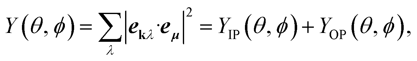

 and ĉnk denote the creation and annihilation operators for an electron in the n-th electronic state with momentum k. The indices m and n run over all the conduction and valence bands, respectively. Overall, with the exciton wave function, the dipole moment of exciton can be obtained. The detail derivatives of the above equations can be found in the ESI.†