
 Open Access Article
 This Open Access Article is licensed under a Creative Commons Attribution-Non Commercial 3.0 Unported Licence
Multiband-switchability and high-absorptivity of a metamaterial perfect absorber based on a plasmonic resonant structure in the near-infrared region
Jian Liang,
Yan Chen *,
Zhangkun Zhou and
Shanjun Chen*
*,
Zhangkun Zhou and
Shanjun Chen*
School of Physics and Optoelectronic Engineering, Yangtze University, Jingzhou, 434023, P. R. China. E-mail: chenyan@yangtzeu.edu.cn; csj@yangtzeu.edu.cn
First published on 28th October 2022
Abstract
Metamaterials are widely studied in bio-photonics because of their flexible and tunable resonance wavelengths in the near-infrared region and their particular relevance to biological tissues. In this paper, we propose for the first time a perfect absorber that is switchable between triple-band and dual-band absorption. The narrowband metamaterial perfect absorber has a conventional metal–dielectric–metal structure, which consists of an array of silver disks, a silica dielectric layer and a gold substrate. Its working performance is mainly determined by the height, radius and period of the top silver disks. By adjusting these parameters, the perfect absorber can be switched between triple-band and dual-band absorption with the peaks showing close to 100% absorbance. This makes it possible to use it as a multifunctional absorber in various applications, such as filters and sensors.
1. Introduction
Metamaterials are artificial materials with properties that are dependent on their subwavelength structure, rather than on their chemical composition, and they have some unique properties not found in naturally occurring materials.1–3 Increasing attention has been paid to perfect absorbers (PA) that are based on metamaterials. The study of metamaterial absorbers shows that the surface plasmons (SPs) in metal micro/nano-structures play an important role in the metamaterial perfect absorber (MPA) due to their strong field confinement and enhancement.4 SPs can be classified as propagating surface plasmons (PSPs) and local surface plasmons (LSPs).5–8 PSPs are mainly associated with periodic structures, while LSPs are mainly associated with metal particles whose structural dimensions are much smaller than the wavelength of incident waves.Metamaterial absorbers (MAs) typically consist of three layers in a metal–dielectric–metal (MDM) structure, i.e., the patterned metal antenna and the thick metal mirror layers are separated by a thin dielectric spacer.9–15 The MDM structure is ideal for designing an MPA, for this kind of structure of MPA can store the internal electromagnetic energy and then dissipate it gradually. The unitary structure of the MDM absorber, also known as a meta-atom, primarily has a regular and simple geometry, including squares,16 rectangles,17 crosses18 and circles.19 So far, the studies on these absorbers have extended to various wavelength bands, such as microwave,20,21 terahertz,22–25 long-wave infrared,26 mid-wave infrared27 and visible–near-infrared bands.28 It is worth mentioning that Karmakar et al.25 designed a metamaterial refractive index sensor by making use of the tuning effect of Fano resonance in the THz band in a geometrically symmetric stacked metamaterial. Its features, such as being multifunctional, highly compact, miniaturized and well-integrated make it promising for commercial use in the future. MPAs are also widely studied for their wide range of potential applications, such as energy harvesting,29 thermal emitters,30 detectors,31 and sensors.32,33 Singh et al.33 designed and constructed a novel spanner resonator for the detection of refractive index changes in biological samples. It could also be used to detect other components, such as human blood type, and ethanol and hemoglobin concentrations. In recent years, various structures, including composites consisting of different simple superatomic and multilayer structures, have been proposed to achieve multiband absorption. Hong et al.34 achieved narrow-band absorption using only a silver substrate and silicon particles. However, due to the simple structure and the few adjustable parameters, the performance of the absorber was not very satisfactory. A multifunctional absorber has been designed by Zhang et al.35 The absorber can achieve broadband and narrowband absorption from positive and negative angles of incidence, respectively. However, the design mentioned above will complicate the fabrication and limit the size of the device and its efficiency. This makes industrial manufacturing much more costly and is not conducive to the same level of mass manufacturing. Moreover, most narrowband MPAs have only a single function and are not adjustable for the number of absorption peaks, which greatly limits the use of absorbers. Therefore, a perfect absorber with a simple and versatile structure needs to be invented.
In this paper, we propose a simple MDM structure that can achieve high absorption. In addition, we analyze three different modes by combining electric field intensity images with absorption spectra recorded when varying the structural parameters. To our knowledge, we obtain, for the first time, a switch between triple-band and dual-band absorption peaks in the near-infrared region by adjusting the structural parameters, and a near 100% absorbance for the two peaks as well. This provides a new route to infrared biomolecular detection.
2. Modes and methods
The MDM structural unit of the metamaterial is shown in Fig. 1(a). The finite-difference time-domain (FDTD) method is used to simulate the absorber we designed. The metamaterial absorber structure consists of three layers, as shown in Fig. 1(b). In the proposed MDM structure, the dielectric layer SiO2 is sandwiched in between the top silver array and the bottom gold film. The use of SiO2 will reduce the propagation loss significantly, thereby increasing the propagation length of the surface plasmons. In the visible to near-infrared (NIR) region, silver is placed on the top layer of the structure as an active layer due to its low inherent loss characteristics. The bottom gold film serves as the substrate mainly to prevent the transmission of incident light. The light is incident perpendicularly along the negative direction of the z-axis. The thickness of the Au is larger than the depth of the penetration of electromagnetic waves in the infrared region to ensure the near-zero transmission of incident light. A thin silica dielectric layer separates the two metal layers as an isolator. The radius and the height of the nanodisks are expressed as r and h, respectively, and the period of the array is designated as p. The thickness of the dielectric layer is denoted by d. The permittivity of the Ag, SiO2 and Au layers is as described by Palik.36 Periodic boundary conditions are used in the x- and y-directions, while, in the z-direction, a perfectly matched layers (PML) boundary condition is adopted. The plane wave is incident vertically from the top. In the experiment, the fabrication process is shown in Fig. 2 and the process is as follows: the SiO2 is deposited onto a gold substrate using the conventional electron beam evaporation method.37 A mask (shown in Fig. 2) is placed close to the dielectric layer to form the top Ag disk by using e-beam deposition. Since the structure we designed is simple, we only need to design masks of different structure sizes to realize the adjustment of the parameters of the structure. This scheme can be used in the dual-band and triple-band switching mentioned later. | ||
| Fig. 1 (a) Three-dimensional schematic diagram of the MDM periodic perfect absorber (16 units). (b) Schematic of a single unit of the metamaterial absorber (MA). | ||
 | ||
| Fig. 2 Schematic illustration of the fabrication process for the absorber. | ||
3. Results and analysis
The absorption can be calculated from A = 1 − R − T, where R and T are the reflection and transmission, respectively. When the thickness of the metal plane is larger than the depth of its skin in the near-infrared (NIR) range, the transmission of the proposed structure is almost zero and the absorption is only related to the reflection (R) 38. Therefore, A = 1 − R − T ≈ 1 − R. The absorption spectrum of the proposed MDM structure is shown in Fig. 3. We denote the three absorption peaks in order of increasing wavelength as mode 1, mode 2 and mode 3, respectively. At λ1 = 783 nm, the absorbance is 99.5%. The full width at half maximum (FWHM) is about 12 nm. Two other absorption bands appear at λ2 = 977 nm and λ3 = 1166 nm with absorbance values as high as 88.9% and 99.4%, respectively. The results of our parameter optimization are shown in Fig. 4. | ||
| Fig. 3 Absorption spectra of triple-band absorption. The radius and height of the silver particles are r = 345 nm and h = 80 nm, respectively. The height of the intermediate medium is d = 85 nm. | ||
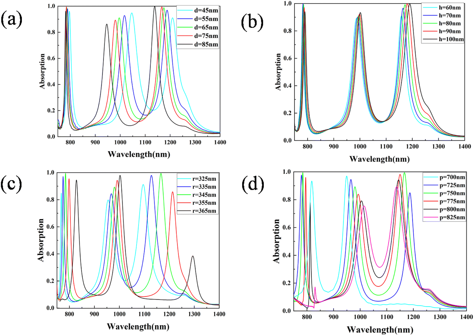 | ||
| Fig. 4 The relationship between dielectric thickness d (a), the thickness h and the radius r of the silver particles (b) and (c), the period p of the silver array (d) and the absorption rate. Parameters: (a) r = 345 nm, p = 750 nm, h = 85 nm. (b) d = 80 nm, r = 345 nm, p = 750 nm. (c) h = 85 nm, d = 85 nm, p = 750 nm. (d) h = 85 nm, d = 80 nm, r = 345 nm. | ||
In the case of a plane wave incident perpendicularly, the position of the PSP mode in the periodic structure can be obtained using the following formula:39,40
 | (1) |
The formation of mode 2 is the result of coupling between the PSPs and LSPs, but is mainly due to the LSPs. A more pronounced blue-shift with an increase in d is illustrated in Fig. 4(a), but the absorption rate does not change any more. This is because the change in dielectric layer thickness can only change the phase of light in the dielectric layer,44 so the effect on the absorption rate is not significant. Fig. 4(c) shows that when the radius of the top layer increases, the absorption peak is red-shifted and the absorbance increases. When the period increases, the absorption peak is red-shifted and the absorbance decreases. This is mainly due to the fact that this mode is formed by the coupling of the PSPs and LSPs. Increasing the top radius and decreasing the period will cause an increase in the particle spacing and an increase in propagating surface plasmons. As a result, it will lead to an increase in the absorption rate.
For mode 3, the gap mode plays a major role. Unlike mode 1, the gap mode here is mainly the result of the interaction between the particles and the gold film. As we can see from Fig. 4(a and b), changing d has a notable effect on the phase of the absorption peak. The change in d also causes a blue-shift of the absorption peak, but has little effect on the absorption rate. On the other hand, however, changing h has little effect on either. We can see from Fig. 4(c) that the absorption peak of mode 3 is red-shifted, and the absorption increases first and then decreases. This is consistent with the results of varying p shown in Fig. 4(d). Increasing p leads to a blue-shift of the absorption peak, and then causes the absorption rate to decrease when p reaches 750 nm, indicating that the interparticle interaction becomes weak and leads to the gradual weakening of the gap mode.45 Both larger r and smaller p will decrease the amount of light entering the gap. Therefore, too large a radius or too small a period will cause the gap pattern to disappear.
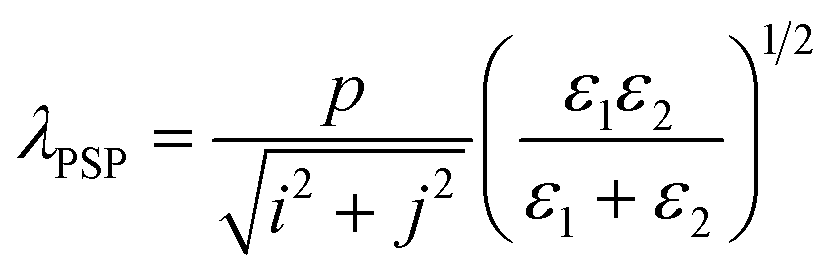
In order to validate the previous analysis of the three modes further, we present Fig. 5 in which the electric and magnetic field intensities are normalized. In the previous section, we determined that mode 1 is the result of the coupling of the PSPs with the gap mode. So, it can be seen that the electric field is distributed in the particle gap, as shown in Fig. 5(a and d). In terms of magnetic field distribution, the gap mode is mainly generated by the gap between silver particles, which confirms the previous statement. It can also be seen in Fig. 5(b and e) that the electric and magnetic fields are localized in the dielectric layer between the silver particles and the gold substrate. This suggests that the main cause of the generation of mode 2 is due to LSPs. Fig. 5(c and f) show that the electric field is distributed in the silver particle gap, while the magnetic field is distributed in the gap that is formed between adjacent silver particles and the gold film. This indicates that the gap pattern of mode 3 is generated by the silver particles and the gold film. The results of the three modes are consistent with those of the previous analysis.
 | ||
| Fig. 5 Normalized electric field (a)–(c) and magnetic field (d)–(f) intensity distributions of the mode 1, mode 2, and mode 3 light absorption bands at the x0z-plane, respectively. | ||
From Fig. 4(d), when p changes from p = 700 nm to p = 725 nm, there is a sudden change in both mode 1 and mode 3. To understand the exact cause of this pattern, a finer parametric scan is performed in the range of p between p = 700 nm and p = 725 nm in Fig. 6(a). For mode 1, p = 700 nm to 725 nm, the gap mode plays a major role. This results in a blue-shift of the absorption peak. From Fig. 4(d), when p = 725 nm, the PSP mode plays a major role, and then the absorption peak starts to red-shift as the period increases. This result is consistent with the previous analysis. For mode 3, the gap pattern is generated with a large variation in absorption rate. The blue-shift of the absorption peak with increasing period is consistent with previous findings. When p = 700 nm, only two absorption peaks are left. Adjusting to h = 40 nm and d = 60 nm can achieve a dual-band perfect absorber. The absorbance of the two peaks reaches 99.6% and 98.4% for modes 1 and 2, respectively, as shown in Fig. 6(b). In Fig. 3 and 6(b), under specific structural parameters, the best absorption performance is achieved for the triple-band and dual-band absorption, respectively. We can switch between dual-band and triple-band filters simply by adjusting the structural parameters. Fig. 6(c) then shows the effect of reducing the structural period p. As p changes from 696 nm to 694 nm, the absorbance of absorption peak 1 drops sharply, and splitting of absorption peak 2 occurs. This is because of near-field interactions that disrupt the resonance mode and affect the absorption performance of the absorber when the silver particles are too close to each other.46
 | ||
| Fig. 6 (a) The relationship between the period (from 700 nm to 720 nm) and the absorption peaks. (b) A spectrum of dual-band absorption. (c) The relationship between the period (from 690 nm to 698 nm) and the absorption peaks. | ||
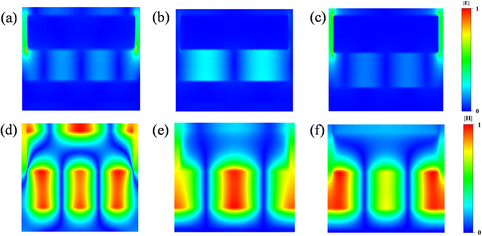
Next, we evaluate two important metrics in sensor applications, namely refractive index sensitivity (S) and figure of merit (FOM) values. S is defined as the ratio of the shift of the resonance peak (Δλ) to the change in refractive index (Δn), i.e., S = Δλ/Δn. The FOM is expressed as the ratio of S to the full width at half maximum (FWHM) of the resonant mode, i.e., FOM = S/FWHM. Fig. 7(a) demonstrates the effect of changing the refractive index from 1 to 1.05 on the absorption spectrum. It is shown that the results of mode 1 with low variations in absorbance and minimal FWHM values are relatively better than the results for the other two modes. Fig. 7(b) shows the mode 1 absorption peak wavelength versus refractive index, where a good linear approximation exists. By calculating the slope of the fitted straight line, a sensitivity of 551 nm per refractive index unit (RIU) is determined. The value of the FWHM is 12 nm, and the calculated value of the FOM is 46. It is important that a versatile perfect absorber can switch between different numbers of absorption peaks to have a good sensing performance.
 | ||
| Fig. 7 (a) The relationship between the refractive index and the absorption peaks. (b) The relationship between the wavelength of the absorption peak (mode 1) and the refractive index. | ||
Finally, in order to understand the inner physical mechanism of the perfect absorption, we give the simulation results of the equivalent electromagnetic parameters for the metamaterial, as shown in Fig. 8. Fig. 8(a–d) show the permittivity, permeability, impedance and refractive index, respectively, as functions of the wavelength. From the impedance matching theory, surface plasmons are generated when the absorber matches the impedance of free space (Z = Z0).47 That is to say, as the impedance of the real part is close to 1 and the imaginary part is close to 0, the higher the absorption of the structure will be. The results of Fig. 8(c) are basically the same as the absorption curve. Therefore, this explains the physical mechanism of perfect absorption theoretically.
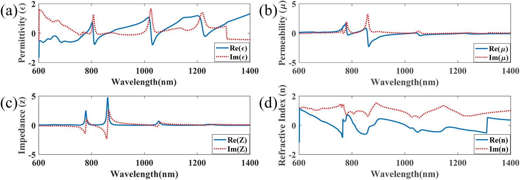 | ||
| Fig. 8 The simulation results for the metamaterial of permittivity (a), permeability (b), impedance (c) and refractive index (d). | ||
4. Conclusions
In this study, we have proposed a metamaterial perfect absorber with a simple structure and a high absorption rate, which allows for dual- and triple-band switching. The absorber is composed of three layers of metal–dielectric–metal. The simple structure makes it conducive to industrial manufacturing. By combining electric field images with absorption spectra recorded when varying the structural parameters, we have analyzed the patterns of the three absorption peaks. By adjusting the parameters, dual-band and triple-band switching can be realized, and the absorbance of two peaks can approach 100%. We have proposed a new direction and an idea for a multifunctional perfect absorber. The multifunctional absorber can be used for filters, biosensing or other photonic devices.Author contributions
Jian Liang: investigation, methodology, software, validation, formal analysis, writing – original draft, writing – review & editing. Yan Chen: investigation, methodology, software, validation, formal analysis, conceptualization, supervision, writing – review & editing. Zhangkun Zhou: formal analysis, data curation, writing – review & editing. Shanjun Chen: conceptualization, supervision, writing – review & editing, funding acquisition.Conflicts of interest
The authors declare that they have no known competing financial interests or personal relationships that could have appeared to influence the work reported in this paper.Acknowledgements
This work was supported by the National Natural Science Foundation of China (No. 91961107). The authors would like to thank Prof. Liping Fu and doctoral candidate Jingyu Wang for some help during the preparation of this paper.References
- D. Schurig, J. J. Mock, B. J. Justice, S. A. Cummer, J. B. Pendry, A. F. Starr and D. R. Smith, Metamaterial electromagnetic cloak at microwave frequencies, Science, 2006, 314, 977–980 CrossRef CAS PubMed.
- H. T. Chen, H. T. Chen, W. J. Padilla, W. J. Padilla, J. M. O. Zide, J. M. O. Zide, A. C. Gossard, A. C. Gossard, A. J. Taylor, A. J. Taylor, R. D. Averitt and R. D. Averitt, Active terahertz metamaterial devices, Nature, 2006, 444, 597–600 CrossRef CAS PubMed.
- R. Sharma and H. Singh, Left handed material antenna design for gsm 1.8 GHz applications, Proceedings of 2015 RAECS UIET Panjab University Chandigarh 21-22nd December, 2015 Search PubMed.
- Y. Chen, S. Chen, T. M. Shih, J. Y. Wang, W. Y. Li, H. Qian and Z. L. Yang, Broadband unidirectional scattering in visible ranges and controllable hot-spot spatial transfer via a single nanoparticle, Appl. Surf. Sci., 2020, 528, 146489 CrossRef CAS.
- Y. Jung, I. H. wang, J. Yu, J. Lee, J. H. Choi, J. H. Jeong, J. Y. Jung and J. Lee, Fano metamaterials on nanopedestals for plasmon-enhanced infrared spectroscopy, Sci. Rep., 2019, 9, 7834 CrossRef PubMed.
- A. V. Zayats and I. I. Smolyaninov, Near-field photonics: surface plasmon polaritons and localized surface plasmons, J. Opt. A: Pure Appl. Opt., 2003, 5, S16–S50 CrossRef CAS.
- H. Raether, Surface plasmons on smooth and rough surfaces and on gratings, Springer Tracts Mod. Phys., 1988, 111, 1–133 Search PubMed.
- M. Nishida, N. Hatakenaka and Y. Kadoya, Multipole surface plasmons in metallic nanohole arrays, Phys. Rev. B: Condens. Matter Mater. Phys., 2015, 91, 235406 CrossRef.
- S. A. Maier, Plasmonics: fundamentals and applications, Springer Berlin, 2007 Search PubMed.
- Z. Yong, S. Zhang, C. Gong and S. He, Narrow band perfect absorber for maximum localized magnetic and electric field enhancement and sensing applications, Sci. Rep., 2016, 6, 24063 CrossRef CAS PubMed.
- K. Q. Le, Q. M. Ngo and T. K. Nguyen, Nanostructured metal–insulator–metal metamaterials for refractive index biosensing applications: Design fabrication, and characterization, IEEE J. Sel. Top. Quantum Electron., 2017, 23, 388–393 Search PubMed.
- K. Q. Le, J. Bai, Q. M. Ngo and P. Chen, Fabrication and numerical characterization of infrared metamaterial absorbers for refractometric biosensors, J. Electron. Mater., 2017, 46, 668–676 CrossRef CAS.
- K. Bhattarai, S. Silva, K. Song, A. Urbas, S. J. Lee, Z. Ku and J. Zhou, Metamaterial perfect absorber analyzed by a meta-cavity mode consisting of multilayer metasurfaces, Sci. Rep., 2017, 7, 10569 CrossRef PubMed.
- Z. Yong, S. Zhang, C. Gong and S. He, Narrow band perfect absorber for maximum localized magnetic and electric field enhancement and sensing applications, Sci. Rep., 2016, 6, 24063 CrossRef CAS PubMed.
- L. X. Li, X. Y. Zong and Y. F. Liu, All-metallic metasurfaces towards high performance magneto-plasmonic sensing devices, Photonics Res., 2020, 8, 1742–1748 CrossRef CAS.
- T. Maier and H. Bruckl, Wavelength-tunable microbolometers with metamaterial absorbers, Opt. Lett., 2009, 34, 3012–3014 CrossRef PubMed.
- Y. M. Wu, F. Tang, J. Chen, S. H. Shang, J. J. Wu, S. J. Chen, Y. Chen, X. Ye and L. M. Yang, Design of high-efficiency all-dielectric polymer meta-surfaces beam deflection blazed grating, Results Phys., 2020, 17, 103094 CrossRef.
- H. Singh, B. S. Sohi and A. Gupta, Designing and analysis of cross-shaped CRLH metamaterial for wide band negative index characteristics, Mater. Res. Express, 2019, 6, 075801 CrossRef CAS.
- N. Liu, M. Mesch, T. Weiss, M. Hentschel and H. Giessen, Infrared perfect absorber and its application as plasmonic sensor, Nano Lett., 2010, 10, 2342–2348 CAS.
- X. Chen, W. Li, Z. Wu, Z. Zhang and Y. Zou, Origami-based microwave absorber with a reconfigurable bandwidth, Opt. Lett., 2021, 46, 1349–1352 CrossRef PubMed.
- J. W. Rao, Y. T. Zhao, Y. S. Gui, X. L. Fan, D. S. Xue and C. M. Hu, Controlling Microwaves in Non-Hermitian Metamaterials, Phys. Rev. Appl., 2021, 15, L021003 CrossRef CAS.
- Z. P. Zheng, Y. Luo, H. Yang, Z. Yi, J. G. Zhang, Q. J. Song, W. X. Yang, C. Liu, X. W. Wu and P. H. Wu, Thermal tuning of terahertz metamaterial properties based on phase change material vanadium dioxide, Phys. Chem. Chem. Phys., 2022, 24, 8846–8853 RSC.
- C. Du, D. Zhou, H. H. Guo, Y. Q. Pang, H. Y. Shi, W. F. Liu, J. Z. Su, C. Singh, S. Trukhanov, A. Trukhanov, L. Panina and Z. Xu, An ultra-broadband terahertz metamaterial coherent absorber using multilayer electric ring resonator structures based on anti-reflection coating, Nanoscale, 2020, 12, 9769–9775 CAS.
- X. Cheng, R. Huang, J. Xu and X. Xu, Broadband Terahertz Near-Perfect Absorbers, ACS Appl. Mater. Interfaces, 2020, 12, 33352–33360 CrossRef CAS PubMed.
- S. Karmakar, D. Kumar, R. K. Varshney and D. R. Chowdhury, Strong Terahertz Matter Interaction Induced Ultrasensitive Sensing in Fano Cavity based Stacked Metamaterials, J. Phys. D: Appl. Phys., 2020, 53, 415101 CrossRef CAS.
- R. L. Paldi, X. Sun, X. Wang, X. Zhang and H. Wang, Strain-Driven In-plane Ordering in Vertically Aligned ZnO-Au Nanocomposites with Highly Correlated Metamaterial Properties, ACS Omega, 2020, 5, 2234–2241 CrossRef CAS PubMed.
- A. Krishna, J. M. Kim, J. Leem, M. C. Wang, S. Nam and J. Lee, Ultraviolet to Mid-Infrared Emissivity Control by Mechanically Reconfigurable Graphene, Nano Lett., 2019, 19, 5086–5092 CrossRef CAS PubMed.
- N. Lee, T. Kim, J. S. Lim, I. Chang and H. H. Cho, Metamaterial-Selective Emitter for Maximizing Infrared Camouflage Performance with Energy Dissipation, ACS Appl. Mater. Interfaces, 2019, 11, 21250–21257 CrossRef CAS PubMed.
- Z. K. Zhou, Y. Chen, Y. H. Tian, J. Liang and W. X. Yang, Ultra-broadband metamaterial perfect solar absorber with polarization-independent and large incident angle-insensitive, Opt. Laser Technol., 2022, 156, 108591 CrossRef CAS.
- C. F. Guo, T. Y. Sun, F. Cao, Q. Liu and Z. F. Ren, Metallic nanostructures for light trapping in energy-harvesting devices, Light: Sci. Appl., 2014, 3, e161 CrossRef.
- W. Li and J. Valentine, Metamaterial perfect absorber based hot electron photodetection, Nano Lett., 2014, 14, 3510–3514 CrossRef CAS PubMed.
- Y. Wang, G. Zhu, M. Li, H. Singh, C. Marques, R. Min, B. K. Kaushik, B. Y. Zhang, R. Jha and S. Kumar, Water Pollutants p-Cresol Detection Based on Au-ZnO Nanoparticles Modified Tapered Optical Fiber, IEEE Trans. Nanobiosci., 2021, 20, 377–384 Search PubMed.
- H. Singh, A. Gupta, R. S. Kaler, S. Singh and A. S. Gill, Designing and Analysis of Ultrathin Metamaterial Absorber for W Band Biomedical Sensing Application, IEEE Sens. J., 2022, 22, 10524–10531 CAS.
- S. Hong, Y. J. Lee, K. Moon and S. H. Kwon, Double Resonance Perfect Absorptionin a Dielectric Nanoparticle Array, Curr. Opt. Photonics, 2017, 1, 228–232 CAS.
- B. L. Zhang, Z. X. Li, Z. D. Hu, J. J. Zhang and J. C. Wang, Analysis of a bidirectional metamaterial perfect absorber with band-switchability for multifunctional optical applications, Results Phys., 2022, 34, 105313 CrossRef.
- E. D. Palik, Handbook of Optical Constants of Solids, Academic press, 1985 Search PubMed.
- H. Luo, Q. Y. Shangguan, Y. T. Yi, S. B. Cheng, Y. G. Yi and Z. Z. Li, A tunable “Ancient Coin”-type perfect absorber with high refractive index sensitivity and good angular polarization tolerance, Coatings, 2021, 11, 814 CrossRef CAS.
- J. Yu, J. Zhu, S. Ye and X. Wang, Ultra-wide sensing range plasmonic refractive index sensor based on a two-dimensional circular-hole grating engraved on a gold film, Results Phys., 2021, 26, 104396 CrossRef.
- W. L. Barnes, A. Dereux and T. W. Ebbesen, Surface plasmon subwavelength optics, Nature, 2003, 424, 824–830 CAS.
- N. Gupta and A. Dhawan, Bridged-bowtie and cross bridged-bowtie nanohole arrays as SERS substrates with hotspot tunability and multi-wavelength SERS response, Opt. Express, 2018, 26, 17899 CrossRef CAS PubMed.
- K. J. Russella and L. Evelyn, Gap-mode Plasmonic Nanocavity, Appl. Phys. Lett., 2010, 97, 163115 CrossRef.
- Z. Q. Wu, J. L. Yang, N. K. Manjunath, Y. J. Zhang, S. R. Feng, Y. H. Lu, J. H. Wu, W. W. Zhao, C. Y. Qiu, J. F. Li and S. S. Lin, Gap-Mode Surface-Plasmon-Enhanced Photoluminescence and Photoresponse of MoS2, Adv. Mater., 2018, 30, 1706527 CrossRef PubMed.
- J. Xu, Z. Zhao, H. Yu, L. Yang, P. Gou, J. Cao, Y. Zou, J. Qian, T. Shi, Q. Ren and Z. An, Design of triple-band metamaterial absorbers with refractive index sensitivity at infrared frequencies, Opt. Express, 2016, 24, 25742–25751 CAS.
- J.-Y. Jung, J. Lee, J.-H. Choi, D.-G. Choi and J.-H. Jeong, Enhancement of refractive index sensing for an infrared plasmonic metamaterial absorber with a nanogap, Opt. Express, 2021, 29, 22796–22804 CrossRef CAS PubMed.
- Y. F. C. Chau, C. K. Wang, L. Shen, C. M. Lim, H. P. Chiang, C. T. C. Chao, H. J. Huang, C. T. Lin, N. T. R. N. Kumara and N. Y. Voo, Simultaneous realization of high sensing sensitivity and tunability in plasmonic nanostructures arrays, Sci. Rep., 2017, 7, 16817 CrossRef PubMed.
- Z. Y. Wang, Y. P. Xu, F. Chen, S. B. Cheng, Z. Yi, G. H. Xiao, Y. H. Li, J. B. Jiang, X. W. Zhou and Z. Y. Chen, Tunable multi-narrowband perfect absorber based on graphene and black phosphorus metamaterial, Optik, 2022, 270, 169932 CrossRef CAS.
- H. Singh, B. S. Sohil and A. Gupta, Designing and analysis of cross-shaped CRLH metamaterial for wide band negative index characteristics, Mater. Res. Express, 2019, 6, 075801 CrossRef CAS.
| This journal is © The Royal Society of Chemistry 2022 |