DOI:
10.1039/D2RA05310A
(Paper)
RSC Adv., 2022,
12, 30838-30845
DFT investigation of the electronic and optical properties of hexagonal MX2/ZrXO (M = W, Mo and X = S, Se) van der Waals heterostructures for photovoltaic solar cell application†
Received
24th August 2022
, Accepted 17th October 2022
First published on 27th October 2022
Abstract
The van der Waals heterostructure of Janus materials with a TMD monolayer was used to create a two-dimensional class of nanomaterials for photovoltaic solar cell applications. It is one of the potential methods for enhancing the performance of photovoltaic systems. Two monolayers of different 2D materials, Janus (ZrXO) and TMDs (MX2), are stacked together to form the heterojunction. Based on density functional theory structural, electrical, and optical properties were investigated. The favorable stacking and stability of the MX2/ZrXO (M = W, Mo and X = S, Se) van der Waals heterostructures are confirmed through binding energies, phonon dispersion and ab initio molecular dynamics calculations. Standard excitonic peaks, which correspond to the bound valence-band hole and conduction-band electron, as well as excitonic peaks involving the mid-gap charges, can be seen in the system's computed absorption spectrum. MX2/ZrXO van der Waals heterostructures are excellent photovoltaic candidates with a maximum achived power conversion efficiency of above 22%. Furthermore, we discovered that the heterostructure materials have a high absorption efficiency which is good for the intended photovoltaic solar cell application.
Introduction
Solar energy has emerged as one of the best energy technology options because it is a renewable, environmentally friendly, cheap1 and readily available source of energy.2 Solar energy boosts the level of sustainable development3 Solar energy technology has been adopted as a means for improving developing countries' economic conditions.4 A photovoltaic and photocatalytic system is a device that uses solar energy to generate electrical and chemical energy, respectively. The majority of hydrogen produced today comes from non-renewable sources such as oil, natural gas, and coal.5 To generate chemical and electrical energy from sunlight using solar photovoltaic and photocatalytic systems is a key strategy for meeting the world's energy demand.6 To achieve this, it is necessary to design semiconductor materials having an appropriate band gap to absorb visible light and generate free electrons.7,8 It is very desirable with today's PV and PC technologies to not only control the semiconductor properties, but also to minimize the related devices into near-atomically thin sizes.9
Following the discovery of graphene,10 scientists focused on two-dimensional (2D) layered materials. 2D materials have a layered crystal structure with strong covalent in-plane bonding and layers that are held together through weak van der Waals (vdW) forces.9 This invention has made study on the development, production and application of 2D materials possible. The quantum confinement of material from their bulk three-dimensional counterpart to a single layer two-dimensional counterpart drastically alters their mechanical and electrical properties so this is one way to tune the properties of 2D materials.11 Beyond graphene, 2D transition-metal dichalcogenides (TMDs) are a broad category of 2D materials having the chemical composition formula MX2, where (M is Nb, W, Mo, etc. are a transition metal atom, and X is Se, S & Te a chalcogen atom). This class of materials have attracted the interest of the scientific community in recent decades due to their distinctive properties including, outstanding electronic and optical characteristics, and extensive application prospects.12–16
In 2017 (ref. 17) a new type of 2D material Janus structures with the chemical formula MXY were created by substituting chalcogen atoms on one side of an MX2 monolayer.18,19 MoSSe was initially synthesized by replacing the S atoms on one side single-layer of MoS2 with Se atoms by chemical vapor deposition which significantly changes the electronic characteristics which leads to, excellent and superior physical properties than MoS2.20,21 For example, the material Janus SMoSe demonstrated high basal plane hydrogen evolution reaction catalytic activity in comparison to MoS2.22 Janus materials have two opposing sides or faces that are exposed.23 Because their broken symmetry destroys the symmetry of the original crystal structure, 2D Janus materials exhibit versatile properties include out-of-plane asymmetry which leads to intrinsic polarity, magnetism, piezoelectricity and Rashba-type spin splitting.12,24–26 This special kind of remarkable features of 2D Janus materials drew a lot of attention and theoretical and experimental results indicate these properties indeed exist in this class of materials.27 Especially the intrinsic polarity is good for efficient separation of photo excited carriers which is good to improve the performance of photovoltaic solar cell.
There has recently been an increase in the number of studies describing the integration of 2D materials with other two-dimensional materials to make van der Waals (vdWs) heterostructures. This structures are currently being extensively explored for a range of uses, including photocatalyst,16 Photovoltaic28 optoelectronics,29 due to its unique monolayer structure which displayed certain novel future such as intrinsic polarization, unique interlayer coupling and sufficient redox potential.29–31 According to current research the structural, electrical, and optical properties of a 2D vdW heterostructure made up of two or more different layered materials are noticeably superior than those of a single material. This increases the possibility of novel properties.28
Despite the fact that various heterostructure are expected to be viable options for the fabrication of high performance photovoltaic materials, but their efficiency is not yet at the desired level. Hence, research into various 2D heterostructures material is critical for better understanding their properties and finding more efficient material which can produce amazing results across the interface.30–32 As a result, it is of significant interest to investigate new 2D materials which might have strong photovoltaic properties. The investigation of various forms of 2D heterostructure material is critical for the advancement of PV efficiency. The unique structural, electrical, and optical features expected from coupling Janus with TMDs monolayer is beneficial to improve performance of this applications. In order to address these issues, we proposed two-dimensional heterostructures constructed from MX2/ZrXO (where, M is Mo, W and X is S, Se). This paper presents in addition to constructing the heterostructures, investigating the materials electrical and optical properties and assessing their application for photovoltaic solar cell.
Computational method
Density functional theory (DFT), as implemented in the Vienna ab initio simulation package (VASP), is used to examine the structural, electrical, and optical properties of the van dar Waals heterostructure MX2/ZrXO.33 Based on generalized gradient approximation (GGA), the Perdew–Burke–Ernzerhof (PBE) functional was employed for the explanation of the exchange correlation functional.32,34–36 For the plane wave basis set, we use 520 eV as the cut-off energy and 9 × 9 × 1 Monkhorst–Pack k-points for geometry optimization.37 Structures are relaxed until forces are less than 0.02 V Å−1. The Grimme DFT-D2 method is used to correct the van der Waals interactions. A vacuum space of 25 Å is set to avoid the interaction between layers caused by the periodic boundary condition. The hybrid Heyd–Scuseria–Ernzerhof (HSE) functional with 25% of the short-range exact exchange is used to account for the underestimation of the band gap for the PBE functional.35 The first Brillouin zone was sampled using a Γ-cantered k-point grid of 15 × 15 × 1 (ref. 38 and 39) and the electronic structure and optical properties of MX2/ZrXO van der Waals heterostructures are then computed. SCF electronic structure calculations included spin orbital coupling (SOC) effects. The phonon calculations were performed in VASP using the PHONOPY40 code in conjunction with the density functional perturbation theory (DFPT) method, and ab initio molecular dynamics (MD) simulations were performed to validate the stabilities at room temperature. At 300 K, MD simulation was completed in 5 ps with a time step of 1.0 fs.41
Result and discussion
Initially, the structure of monolayer ZrXO and MX2 is prepared. The hexagonal and distorted monolayer geometry has been optimized. The optimal lattice parameter of the single monolayer ZrXO (ZrSO, ZrSeO) and MX2 (WS2, MoS2, MoSe2, WSe2) is 3.35 Å, 3.40 Å, 3.20 Å, 3.20 Å, 3.30 Å, 3.30 Å respectively, the obtained values are comparable to the prior result.42–46 The optimized lattice parameter and total energy for hexagonal and distorted monolayers are shown in Table 1.
Table 1 Optimized lattice parameter and total energy for hexagonal and distorted monolayers
| |
Monolayer |
Lattice parameter (Å) |
Total energy (eV) |
| Hexagonal a = b ≠ c |
H-ZrSO |
3.35 |
|
−22.771315 |
| H-ZrSeO |
3.40 |
|
−21.912457 |
| H-MoS2 |
3.20 |
|
−22.120780 |
| H-WS2 |
3.20 |
|
−22.263496 |
| H-MoSe2 |
3.30 |
|
−20.297765 |
| H-WSe2 |
3.30 |
|
−20.241997 |
| Orthorhombic a ≠ b ≠ c |
T-ZrSO |
3.46 |
5.96 |
−47.344327 |
| T-ZrSeO |
3.50 |
6.0 |
−45.305777 |
| T-MoS2 |
3.18 |
5.68 |
−43.160438 |
| T-WS2 |
3.22 |
5.72 |
−43.466275 |
| T-MoSe2 |
3.34 |
5.84 |
−39.907106 |
| T-WSe2 |
3.34 |
5.84 |
−39.911126 |
In addition to the stability as depicted in Table 2, the selected heterostructures have a lattice mismatch of <5% which means these systems can be fabricated.45 However, all the distorted structure is unstable with positive binding energy, whereas the hexagonal structure is more stable with negative binding energy, so the four hexagonal structures MoSe2/ZrSeO, WS2/ZrSO, MoS2/ZrSO and WSe2/ZrSeO are used in the following studies Table 2 contains a list of the results.
| | |
Eb = EHetro − EJanus − ETMD
| (1) |
where,
Eb is the binding energy,
EHetro,
EJanus,
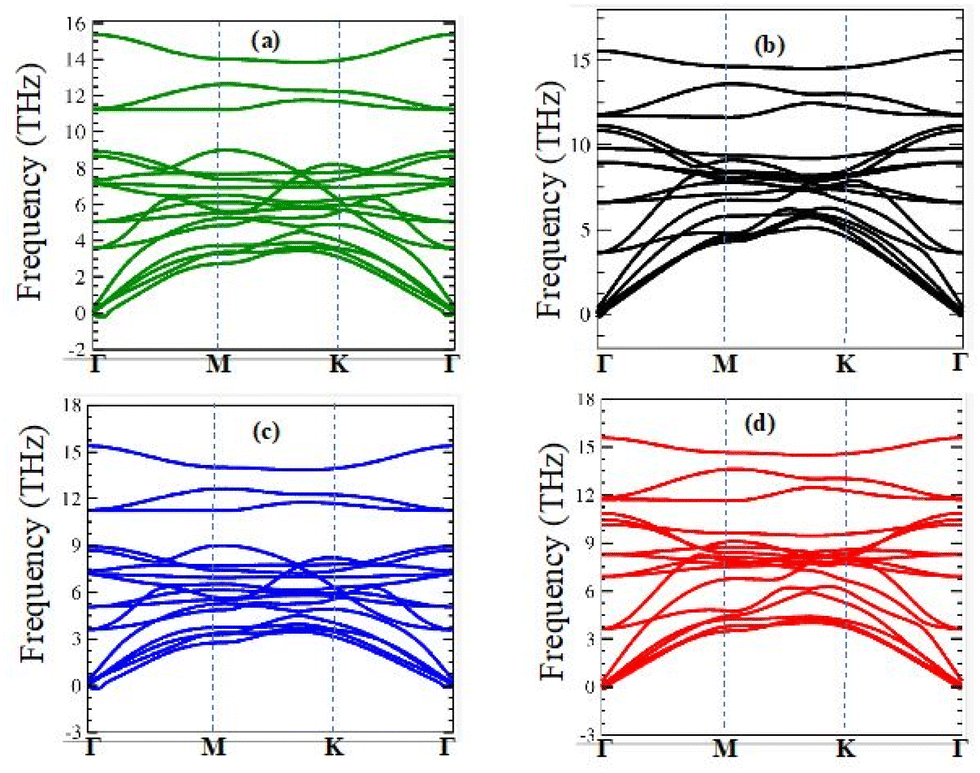
ETMD are the heterostructure, Janus and TMD total energy, respectively. The dynamical stability of the MX
2/ZrXO vdW heterostructure was confirmed further by computing their vibrational spectra, as shown in
Fig. 1(a)–(d). The absence of imaginary frequencies demonstrates that all MX
2/ZrXO heterostructures are dynamically stable. Furthermore, at 300 K,
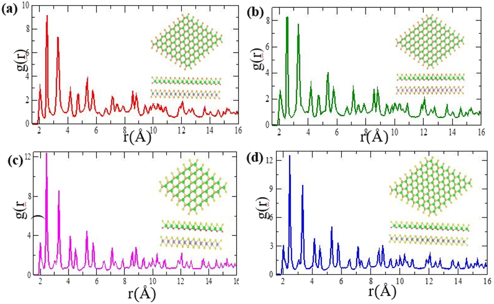
ab initio molecular dynamics (AIMD) simulations of MX
2/ZrXO vdW heterostructures were performed for 5 ps with a time step of 1.0 fs. Radial distribution functions (RDFs) are commonly used in simulations to represent the spatial organization of ions around a central ion. They can also be derived indirectly using X-ray spectra. Solids have regular, periodic structures with molecules that fluctuate near the lattice. Defects in solids are uncommon because the structure is extremely long-range. The shape of each peak is distorted by particles bouncing around their lattice locations. Between these peaks, there is little prospect of finding a particle because every molecule is packed uniformly to fill the space as completely as possible. The nearest neighbors are in the first coordination shell of a solid, the second in the second, and so on. Each peak symbolizes a solid's coordination shell. Near their lattice sites, molecules vary in solids with regular, periodic forms. Solids rarely have flaws because of their highly long-range structure. There is no prospect of discovering a particle between their peaks because every molecule is packed uniformly to occupy the space most effectively. The nearest neighbors are in the first shell, the second in the second, and so on, with each peak representing the coordination shell of a solid. RDFs is defined as the probability density of finding an atom at a randomly chosen point
r from a central atom divided by the mean number density. Hence, radial distribution function (RDF) is defined by
g(
r) =
n(
r)/4π
r2Δ
ρo, where
n(
r) fluctuates around but on average approaches 4π
r2ρo at large
r, where
ρo is the mean number density. The AIMD simulations were performed to confirm the thermal stability of ZrXO (ZrSO, ZrSeO) and MX
2 (WS
2, MoS
2, MoSe
2, WSe
2) vdW heterostructure as shown in
Fig. 2(a)–(d) and it shows thermal stabilities with no structural degradation at 300 K.
Fig. 2(a) indicates the radial distribution functions,
g(
r), for the probability density of MoSe
2/ZrSeO of pair correlation function between Zr–O, Zr–Se and Mo–Se are 2.056 Å, 2.588 Å and 3.275 Å, respectively. As shown in
Fig. 2(b) MoS
2/ZrSO of pair correlation function are 2.033 Å, 2.564 Å and 3.325 Å for Zr–O, Zr–Se and Mo–Se, respectively. For WSe
2/ZrSeO vdW heterostructure of pair correlation function are 2.074 Å, 2.539 Å and 3.372 Å for Zr–O, Zr–Se and Mo–Se, respectively is shown in
Fig. 2(c). As illustrated in shown in
Fig. 2(d) the pair correlation function between Zr–O, Zr–Se and Mo–Se are 2.024 Å, 2.515 Å and 3.323 Å, respectively for MoS
2/ZrSO vdW heterostructure. The sharpness of the second and third peaks reflects the heterostructure, whereas the
g(
r) profile reveals the atom that contributes the most to the system.
Table 2 Contains the heterostructure optimized lattice parameter, binding energy, lattice mismatch, and spacing
| Heterostructures |
Lattice parameter (Å) |
Binding energy (meV) |
Lattice mismatch (%) |
Spacing |
| H-MoSe2/ZrSeO |
3.35 |
−2.704 |
2.94 |
3.625 |
| H-WSe2/ZrSeO |
3.35 |
−1.512 |
2.94 |
3.659 |
| H-MoS2/ZrSO |
3.25 |
−1.368 |
4.48 |
3.659 |
| H-WS2/ZrSO |
3.25 |
−1.265 |
4.48 |
3.633 |
| T-MoSe2/ZrSeO |
3.42 and 5.92 |
68.59 |
— |
3.474 |
| T-WSe2/ZrSeO |
3.42 and 5.92 |
62.578 |
— |
3.990 |
| T-MoS2/ZrSO |
3.34 and 5.84 |
195.468 |
— |
3.616 |
| T-WS2/ZrSO |
3.34 and 5.84 |
25.845 |
— |
4.155 |
 |
| | Fig. 1 Phonon dispersion of (a) MoSe2/ZrSeO, (b) MoS2/ZrSO, (c) WSe2/ZrSeO, and (d) WS2/ZrSO vdW heterostructures in the first Brillouin zone, respectively. | |
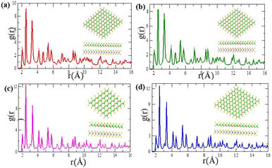 |
| | Fig. 2 Pair correlation functions after a temperature fluctuation of 4900 fs at 300 K for (a) MoSe2/ZrSeO, (b) MoS2/ZrSO, (c) WSe2/ZrSeO, and (d) WS2/ZrSO heterostructures, respectively. | |
We build the heterostructure by stacking the monolayers of ZrXO on MX2. We created six stacking patterns by developing three hexagonal and three deformed stacks, then we plan to choose one from each hexagonal and distorted based on least binding energy using eqn (1).38
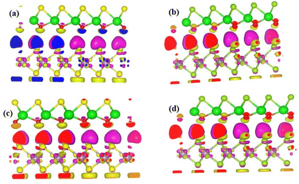
Charge density difference
Charge density difference is an important model to study the properties of atoms and molecules and its interactions.33 As a result, the charge density difference can be used to gain a better understanding of charge transfer in heterostructures at the interface using the form Δρ = ρZrXO/MX2 − ρZrXO − ρMX2 where, ρZrXO/MX2, ρZrXO, and ρMX2 represent the charge densities of the heterostructure, Janus, and MX2 structures, respectively.33,47 Plots of differential charge density for MX2/ZrXO heterostructures are shown in Fig. 3(a)–(d). We can see from the figure there is charge accumulation at the interface area of ZrXO and MX2. It is clear that charge density redistribution is feasible. There is also some charge depletion. The yellow and red isosurfaces represent the accumulation and depletion of electronic densities, respectively.
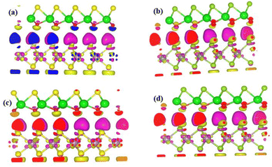 |
| | Fig. 3 (a)–(d) Are plots of partial charge density difference for (a) MoSe2/ZrSeO, (b) WSe2/ZrSeO, (c) MoS2/ZrSO, and (d) WS2/ZrSO vdW heterostructures respectively. Isosurfaces refer to isovalues of 2.95 × 10⁻³ electrons per bohr3. | |
Electronic properties
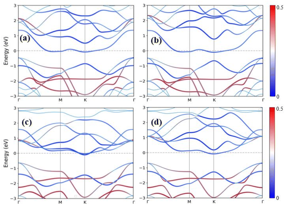
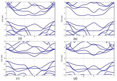
The band gap of the MX2/ZrXO heterostructure was determined using the PBE method, and SOC, as shown in Fig. 4(a)–(d) and for SOC in the ESI Fig. S4(a)–(d).† Regardless of whether SOC effects are taken into account or not, all of the estimated band gaps in the heterostructure are indirect semiconductors except WSe2/ZrSeO vdW heterostructure clearly shown in Fig. 5(c). The band gap of the hexagonal phases of the heterostructure MX2/ZrXO was discovered to be small but we know the PBE level DFT underestimates band gap value. As a result, we used a hybrid functional (HSE06) to get more accurate band gap of MoSe2/ZrSeO, WSe2/ZrSeO, MoS2/ZrSO, and WS2/ZrSO which became 1.0, 1.6, 1.7, and 1.66 eV, respectively, as shown in Fig. 5(a)–(d). For the materials their valence band maximums are all close to the Fermi level. We see an indirect band gap between the conduction band minimum (CBM) and the valence band maximum (VBM) at M and Γ, respectively, for the materials WSe2/ZrSeO, MoS2/ZrSO, and WS2/ZrSO, but the CBM occurs between K and M for the material MoSe2/ZrSeO. Except for MoS2/ZrSO, the valence band maximums of these materials are all close to the Fermi level. This means that the mobility of the hole is greater than that of the electron. As one can obviously see that from the band structure the electronic structure changes significantly after the heterostructure is formed.
 |
| | Fig. 4 Band structures of (a) MoSe2/ZrSeO, (b) MoS2/ZrSO, (c) WSe2/ZrSeO, and (d) WS2/ZrSO vdW heterostructures using PBE functional. The blue and red colors represent the contribution of the s-p and M-d orbitals, respectively. | |
 |
| | Fig. 5 The band structures of (a) MoSe2/ZrSeO, (b) MoS2/ZrSO, (c) WSe2/ZrSeO, and (d) WS2/ZrSO vdW heterostructures using HSE06 functional. | |
Zr–S, Zr–Se, and Zr–O bonds have lengths of 2.561, 2.707, and 2.143 angstrom, respectively. Because the X and O atoms differ in size and electronegativity, the Zr–X and Zr–O bond lengths and dipoles are in-equivalent, causing the mirror symmetry of the Janus ZrXO monolayer to be broken. The Mo–S, W–S, Mo–Se, and W–Se bond lengths in MoS2, WS2, MoSe2, and WSe2 monolayers are 2.429, 2.434, 2.546 and 2.554 angstrom, respectively. Monolayers are almost identical to previously reported values.43–45 Because of the large atomic radius, the system band gap increases as the M-atom in the TMD monolayer is changed from Mo to W.
Optical properties
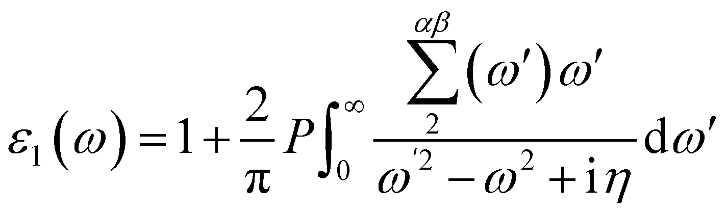
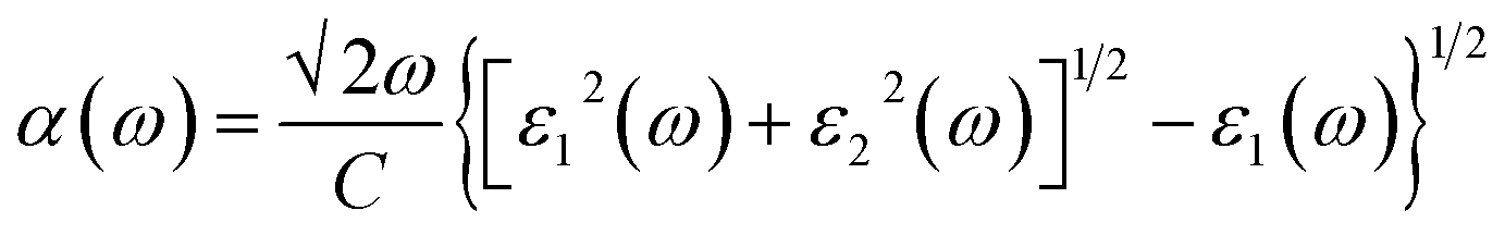
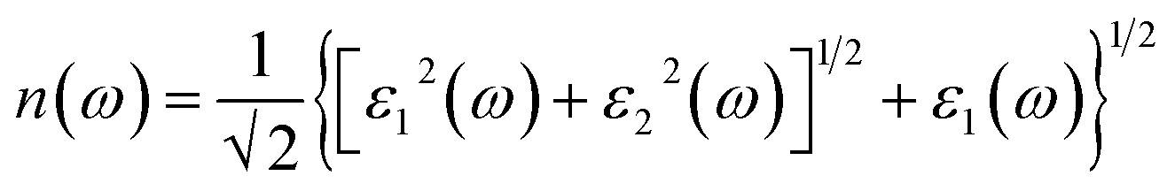
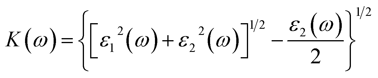
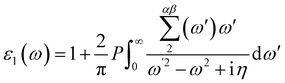
Materials' optical properties are heavily influenced by their structure of electronic bands.48 We have calculated that for 2D hexagonal MX2/ZrXO van der Waals heterostructures absorbance, refractive index, reflectance, and extinction coefficient. The optical properties of a solid are determined using a Kramers–Kronig relation. The complex dielectric response function is used to describe a medium's optical properties ε(ω) = ε1(ω) + iε2(ω) where ε1(ω) represents the real part and ε2(ω) represents the imaginary part. The dielectric function is shown in eqn (2) and (3) by random phase approximation below. The dielectric function gave some other optical constant from eqn (4)–(7) below to calculate the optical properties49–53| |
 | (2) |
| |
 | (3) |
where P, is applied to the eigenfunction momentum operator, the primitive cell's volume is represented by Ω, the electron momentum operator is denoted by q, the conduction band and valence state are denoted by c and v, respectively. ωk represents the k point weight. Eck, Evk and μck, μvk are the eigenvalues and wave function, respectively, at the k point, and eα, eβ are unit vectors for the three cartesian directions. ω is in energy units, the frequency of electromagnetic (EM) radiation| |
 | (4) |
| |
 | (5) |
| |
 | (6) |
| |
 | (7) |
where, α(ω), n(ω), R(ω), and K(ω) are absorption coefficient, refractive index, reflectance and extinction coefficient respectively.
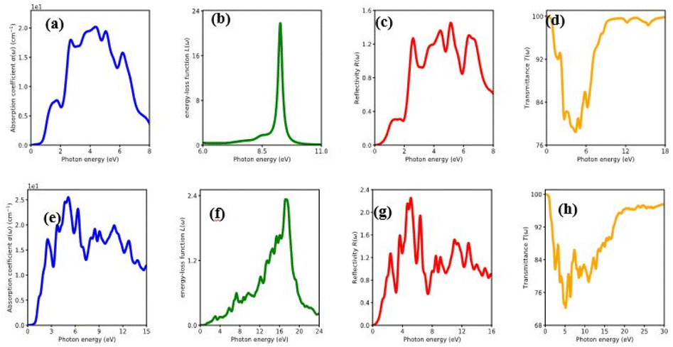
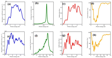
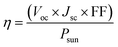
The percentage of light absorbed at a given frequency in these two-dimensional materials is depicts in Fig. 6(a)–(h) and 7(a)–(h). The absorption coefficient determines how far a light beam can penetrate in a given material. Within the studied energy range, there are multiple peaks. Which demonstrates the heterostructure's improved out of plane optical absorption over a single monolayer. MX2/ZrXO is an excellent absorber of visible light. The peak value of absorption changes significantly when we shift from MoX2/ZrXO to WX2/ZrXO. The four hexagonal heterostructures has the highest value in the visible-UV region, but among the materials, ZrSO/MoS2 is slightly better in the visible regions than the others. The heterostructure shows increased optical absorption for visible light. The optical transitions of filled levels to empty ones at 2.15–5.23 eV are represented by the MX2/ZrXO vdW heterostructure. At 2.15 eV, the interband transition (shown in Fig. 6 and 7) occurs from the valence band to the conduction band along the M- and K-directions. The story is the same at 3.45 eV, with the exception that it is along the M-direction and close to the M point. Transitions occur at 4.2 eV and 5.3 eV, respectively, along the K-symmetry direction and at the M symmetry point. All of the above interband transitions are primarily caused by the X atoms' sp orbital to the M atoms' d orbital.
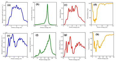 |
| | Fig. 6 Optical property of MoSe2/ZrSeO vdW heterostructure of (a) absorption coefficient, (b) energy loss function, (c) reflectivity and (d) transmittance. MoS2/ZrSO vdW heterostructure of (e) absorption coefficient, (f) energy loss function, (g) reflectivity, (h) transmittance. | |
 |
| | Fig. 7 Optical property of WSe2/ZrSeO vdW heterostructure of (a) absorption coefficient, (b) energy loss function, (c) reflectivity and (d) transmittance. WS2/ZrSO vdW heterostructure of (e) absorption coefficient, (f) energy loss function, (g) reflectivity, (h) transmittance | |
The MX2/ZrXO heterostructure refractive indexes behaviours in the visible light range. The static refractive indexes at n(0) for MoSe2/ZrSeO, WSe2/ZrSeO, MoS2/ZrSO, and WS2/ZrSO, respectively, are 2.68, 2.6, 2.76, and 2.65. The refractive index n(ω) decreases with increasing energy in the visible region. The highest refractive index is for MoS2/ZrSO which has a value of 3.33.
In the visible light region, the reflectance of the heterostructure have a lower value which can be seen in Fig. 6(a)–(h) and 7(a)–(h). The figure depicts the variation in reflectivity with regard to energy, with several peaks reflecting up to 8–12 eV. The highest peaks for the materials MoSe2/ZrSeO, WSe2/ZrSeO, MoS2/ZrSO, and WS2/ZrSO are 5.8 eV, 5.2 eV, 5.0 eV, and 5.6 eV, respectively. We can see that the highest peaks occur in different parts of the UV spectrum, which is good for semiconductor materials that operate in the visible-UV range.
Extinction coefficient which represents the medium's total effect on radiation passing through it this extinction coefficient for the heterostructures shown in Fig. 6 and 7. In the visible and UV regions, the spectrum curves of the extinction coefficient K(ω) increased with increasing energy and then decreased.
Photovoltaic solar cell
The photovoltaic efficiency of the given hexagonal MX2/ZrXO van der Waals heterostructures with a different fill factor and potential loss is described in the Table 3 below. The following equations from 8 to 11 used to calculate the photovoltaic conversion efficiency.54,55 The maximum power conversion efficiency of the value for the material MX2/ZrXO is 22.06 percent with a fill factor of 0.57 and a potential loss of 0.2.| |
 | (8) |
where Voc (mV) is open circuit voltage, Jsc is short circuit current, FF is the fill factor, and Psun is solar power representing the total amount of incident solar radiation
Table 3 Shows the calculated photovoltaic efficiency for different values of fill factor and potential loss
| Heterostructures |
Band gap (eV) |
PCE (%) |
| (Fill factor)/(potential loss) = 0.5/0.3 |
(Fill factor)/(potential loss) = 0.5/0.2 |
(Fill factor)/(potential loss) = 0.57/0.3 |
(Fill factor)/(potential loss) = 0.57/0.2 |
| H-MoSe2_ZrSeO |
1.0 |
16.94 |
19.36 |
19.3 |
22.06 |
| H-WSe2_ZrSeO |
1.6 |
16.01 |
17.24 |
18.25 |
19.66 |
| H-ZrSeO_MoS2 |
1.7 |
15.13 |
16.21 |
17.25 |
18.48 |
| H-ZrSeO_WS2 |
1.66 |
15.54 |
16.67 |
17.71 |
19.01 |
The band gap is denoted by Eg, the maximum short-circuit current density is denoted by Jsc, and Jsc is calculated using the NREL AM1.5 dataset.
| |
 | (10) |
Psun is computed using the following equation
| |
 | (11) |
The fill factors in this heterostructure we use 0.5 and 0.57, so we took this into account. For energy loss (Eloss), we use a value of 0.2 and 0.3.56,57
Conclusions
ZrXO and MX2 monolayers are stacked and optimized to form a hexagonal MX2/ZrXO van der Waals heterostructure. Incorporating monolayer MX2 and ZrXO into a MX2/ZrXO layered heterostructure is the best strategy to improve photovoltaic efficiency. The heterostructures was discovered to be a semiconductor with a band gap of 1.0 to 1.7 eV. The heterostructures displayed anisotropic optical behaviour. The materials have a higher absorption coefficient peak in the visible region, this high absorption coefficient and a broad absorption spectrum making them MX2/ZrXO van dar Waals heterostructures have an excellent potential to be used in photovoltaic devices. The presence of strong absorption peaks in the visible-UV region suggests that this material has a high potential for use in photovoltaic materials for solar cells and because the wavelengths of light arriving at earth are mostly in the visible regions, heterostructures are promising for various photocatalytic, photovoltaic, and optical device.
Conflicts of interest
There are no conflicts to declare.
Acknowledgements
This work was supported by a thematic research project (Grant No. TR/036/2020) and thematic research project (Grant No. RD/LT-095/2019) funded by Addis Ababa University. The authors would like to acknowledge the computational resource support from the ICTP-East African Institute for Fundamental Research under the auspices of UNESCO at Kigali, Rwanda and Ethiopian Education and Research Network (EthERNet) at the Ethiopian Ministry of Science and Higher Education. Tamiru Teshome would like to thank Ayan Datta for computational resources. Dr Kingsly's and Mr Sunday Joseph helpful discussions are gratefully acknowledged.
References
- M. K. H. Rabaia, M. A. Abdelkareem, E. T. Sayed, K. Elsaid, K. J. Chae, T. Wilberforce and A. G. Olabi, Sci. Total Environ., 2021, 754, 141989 CrossRef CAS PubMed.
- 2019 4th MEC International Conference on Big Data and Smart City (ICBDSC), IEEE, 2019 Search PubMed.
- T. Güney, International Journal of Sustainable Development and World Ecology, 2022, 29(2), 187–194 CrossRef.
- N. Kannan and D. Vakeesan, Renewable Sustainable Energy Rev., 2016, 62, 1092–1105 CrossRef.
- N. L. Panwar, S. C. Kaushik and S. Kothari, Renewable Sustainable Energy Rev., 2011, 15, 1513–1524 CrossRef.
- E. Kabir, P. Kumar, S. Kumar, A. A. Adelodun and K. H. Kim, Renewable Sustainable Energy Rev., 2018, 82, 894–900 CrossRef.
- B. Parida, S. Iniyan and R. Goic, Renewable Sustainable Energy Rev., 2011, 15, 1625–1636 CrossRef CAS.
- L. Hernández-Callejo, S. Gallardo-Saavedra and V. Alonso-Gómez, Sol. Energy, 2019, 188, 426–440 CrossRef.
- A. Chaves, J. G. Azadani, H. Alsalman, D. R. da Costa, R. Frisenda, A. J. Chaves, S. H. Song, Y. D. Kim, D. He, J. Zhou, A. Castellanos-Gomez, F. M. Peeters, Z. Liu, C. L. Hinkle, S. H. Oh, P. D. Ye, S. J. Koester, Y. H. Lee, P. Avouris, X. Wang and T. Low, npj 2D Mater. Appl., 2020, 4(1), 1–21 CrossRef.
- Q. Tang, Z. Zhou and Z. Chen, Wiley Interdiscip. Rev.: Comput. Mol. Sci., 2015, 5, 360–379 CAS.
- I. Ahmad, I. Shahid, A. Ali, L. Gao and J. Cai, RSC Adv., 2021, 11, 17230–17239 RSC.
- J. Lou, K. Ren, Z. Huang, W. Huo, Z. Zhu and J. Yu, RSC Adv., 2021, 11, 29576–29584 RSC.
- A. A. Kistanov, S. A. Shcherbinin, S. v. Ustiuzhanina, M. Huttula, W. Cao, V. R. Nikitenko and O. v. Prezhdo, J. Phys. Chem. Lett., 2021, 12, 3436–3442 CrossRef CAS PubMed.
- M. Wu, Y. Xiao, Y. Zeng, Y. Zhou, X. Zeng, L. Zhang and W. Liao, InfoMat, 2021, 3, 362–396 CrossRef CAS.
- T. F. Schranghamer, M. Sharma, R. Singh and S. Das, Chem. Soc. Rev., 2021, 50, 11032–11054 RSC.
- P. You, G. Tang and F. Yan, Mater. Today Energy, 2019, 11, 128–158 CrossRef CAS.
- T. Zheng, Y. C. Lin, Y. Yu, P. Valencia-Acuna, A. A. Puretzky, R. Torsi, C. Liu, I. N. Ivanov, G. Duscher, D. B. Geohegan, Z. Ni, K. Xiao and H. Zhao, Nano Lett., 2021, 21, 931–937 CrossRef CAS PubMed.
- A. E. G. Mikkelsen, F. T. Bölle, K. S. Thygesen, T. Vegge and I. E. Castelli, Phys. Rev. Mater., 2021, 5(1), 014002 CrossRef CAS.
- I. Bouziani, M. Kibbou, Z. Haman, N. Khossossi, I. Essaoudi, A. Ainane and R. Ahuja, Phys. E, 2021, 134, 114900 CrossRef CAS.
- N. Zhao and U. Schwingenschlögl, npj 2D Mater. Appl., 2021, 5(1), 1–5 CrossRef.
- Z. Haman, M. Kibbou, I. Bouziani, Y. Benhouria, I. Essaoudi, A. Ainane and R. Ahuja, Phys. B, 2021, 604, 412621 CrossRef CAS.
- J. Zhang, S. Jia, K. Iskandar, L. Dong, D. Er, W. Chen, H. Guo, Z. Jin, V. B. Shenoy, L. Shi and J. Lou, ACS Nano, 2017, 11(8), 8192–8198 CrossRef CAS PubMed.
- V. Montes-García and P. Samorì, Chem. Sci., 2022, 13, 315–328 RSC.
- R. Li, J. Jiang, X. Shi, W. Mi and H. Bai, ACS Appl. Mater. Interfaces, 2021, 13, 38897–38905 CrossRef CAS PubMed.
- T. Yu, C. Wang, X. Yan, G. Yang and U. Schwingenschlögl, J. Phys. Chem. Lett., 2021, 12, 2464–2470 CrossRef CAS PubMed.
- L. Zhang, Y. Gu and A. Du, ACS Omega, 2021, 6, 31919–31925 CrossRef CAS PubMed.
- P. Wang, Y. X. Zong, H. Y. Wen, J. B. Xia and Z. M. Wei, Acta Phys. Sin., 2021, 70(2) DOI:10.7498/aps.70.20201406.
- L. Ju, M. Bie, X. Zhang, X. Chen and L. Kou, Front. Phys., 2021, 16(1) DOI:10.1007/s11467-020-1002-4.
- S. Qi, J. Jiang, X. Wang and W. Mi, Carbon, 2021, 174, 540–555 CrossRef CAS.
- Z. Shen, K. Ren, R. Zheng, Z. Huang, Z. Cui, Z. Zheng and L. Wang, Front. Mater., 2022, 9, 838648 CrossRef.
- Y. Chen and M. Sun, Nanoscale, 2021, 13, 5594–5619 RSC.
- A. Nijamudheen and A. v. Akimov, J. Phys. Chem. C, 2017, 121, 6520–6532 CrossRef CAS.
- F. Ling, W. Kang, H. Jing, W. Zeng, Y. Chen, X. Liu, Y. Zhang, L. Qi, L. Fang and M. Zhou, npj Comput. Mater., 2019, 5(1) DOI:10.1038/s41524-019-0161-8.
- H. K. Neupane and N. P. Adhikari, Computational Condensed Matter, 2020, 24 DOI:10.1016/j.cocom.2020.e00489.
- C. Nguyen, N. v. Hoang, H. v. Phuc, A. Y. Sin and C. v. Nguyen, J. Phys. Chem. Lett., 2021, 12, 5076–5084 CrossRef CAS PubMed.
- J. Qiu, F. Zhang, H. Li, X. Chen, B. Zhu, H. Guo, Z. Ding, J. Bao and J. Yu, IEEE Electron Device Lett., 2021, 42, 561–564 CAS.
- X. P. Wang, X. bin Li, N. K. Chen, J. H. Zhao, Q. D. Chen and H. B. Sun, Phys. Chem. Chem. Phys., 2018, 20, 6945–6950 RSC.
- K. Rahimi, Phys. Chem. Chem. Phys., 2020, 22, 7412–7420 RSC.
- A. Torabi and V. N. Staroverov, J. Phys. Chem. Lett., 2015, 6, 2075–2080 CrossRef CAS PubMed.
- A. Togo and I. Tanaka, Scr. Mater., 2015, 108, 1–5 CrossRef CAS.
- O. I. Malyi, K. V. Sopiha and C. Persson, Energy, phonon, and dynamic stability criteria of 2d, arXiv, 2019 preprint, arXiv:1901.07202 Search PubMed.
- Y. Ji, M. Yang, H. Lin, T. Hou, L. Wang, Y. Li and S. T. Lee, J. Phys. Chem. C, 2018, 122, 3123–3129 CrossRef CAS.
- R. Chaurasiya, A. Dixit and R. Pandey, Superlattices Microstruct., 2018, 122, 268–279 CrossRef CAS.
- Z. Guan, C. S. Lian, S. Hu, S. Ni, J. Li and W. Duan, J. Phys. Chem. C, 2017, 121, 3654–3660 CrossRef CAS.
- Q. Alam, M. Idrees, S. Muhammad, C. v. Nguyen, M. Shafiq, Y. Saeed, H. U. Din and B. Amin, RSC Adv., 2021, 11, 12189–12199 RSC.
- W. Chen, X. Hou, X. Shi and H. Pan, Two-dimensional Janus transition metal oxides and chalcogenides: multifunctional properties for photocatalysts, electronics and energy conversion, 2018 Search PubMed.
- Y. Liu, Y. Huang and X. Duan, Nature, 2019, 567, 323–333 CrossRef CAS PubMed.
- M. Bernardi, C. Ataca, M. Palummo and J. C. Grossman, Nanophotonics, 2017, 6, 479–493 Search PubMed.
- B. Qiu, X. Zhao, G. Hu, W. Yu, J. Ren and X. Yuan, Nanomaterials, 2018, 8(11) DOI:10.3390/nano8110962.
- R. John and B. Merlin, J. Phys. Chem. Solids, 2017, 110, 307–315 CrossRef CAS.
- G. L. Tan, L. K. Denoyer, R. H. French, M. J. Guittet and M. Gautier-Soyer, J. Electron Spectrosc. Relat. Phenom., 2005, 142, 97–103 CrossRef CAS.
- H. Ni, M. Li, Y. Hu, C. Mao, L. Xue, H. Zeng, Z. Yan, Y. Wu and C. Zheng, J. Phys. Chem. Solids, 2019, 131, 223–229 CrossRef CAS.
- H. A. Mezher, K. J. Kadhim and H. Rahman Jappor, Structural, electronic and optical properties of the bilayer SnS2/InSe heterostructures on the basis of monolayers SnS2 and InSe. Isotropic, optoelectronics diodes of SnS2/InSe heterostructures monolayers based on SnS2 and InSe, Journal University of Kerbala, 2019, 17(4) Search PubMed.
- P. K. Nayak, S. Mahesh, H. J. Snaith and D. Cahen, Nat. Rev. Mater., 2019, 4, 269–285 CrossRef CAS.
- M. R. Filip, C. Verdi and F. Giustino, J. Phys. Chem. C, 2015, 119, 25209–25219 CrossRef CAS.
- M. M. Furchi, F. Höller, L. Dobusch, D. K. Polyushkin, S. Schuler and T. Mueller, npj 2D Mater. Appl., 2018, 2(1), 1–7 CrossRef.
- K. Lai, C. L. Yan, L. Q. Gao and W. B. Zhang, J. Phys. Chem. C, 2018, 122, 7656–7663 CrossRef CAS.
|
| This journal is © The Royal Society of Chemistry 2022 |
Click here to see how this site uses Cookies. View our privacy policy here. 
 Open Access Article
 This Open Access Article is licensed under a Creative Commons Attribution-Non Commercial 3.0 Unported Licence
 ad,
Tamiru Teshome
ad,
Tamiru Teshome