
 Open Access Article
 This Open Access Article is licensed under a Creative Commons Attribution-Non Commercial 3.0 Unported Licence
Physicochemically modified high-resolution tin oxide thin film using soft imprinting
Dong Hyun Kima,
Dong Wook Leea,
Jin Young Oha,
Ju Hwan Leea,
Jonghoon Wona,
Jong In Jangbc,
Hae-Chang Jeong*bc and
Dae-Shik Seo *a
*a
aDepartment of Electrical and Electronic Engineering, Information Display Device Laboratory, Yonsei University, 50 Yonsei-ro, Seodaemun-gu, Seoul 120-749, Republic of Korea. E-mail: dsseo@yonsei.ac.kr
bDepartment of Smart Manufacturing Engineering, Changwon National University, 20 Changwondaehak-ro, Changwon, Gyeongnam 51140, Republic of Korea. E-mail: jhchang@changwon.ac.kr
cDepartment of Electrical Electronic and Control Engineering, Changwon National University, 20 Changwondaehak-ro, Changwon, Gyeongnam 51140, Republic of Korea
First published on 20th September 2022
Abstract
We carried out nanoimprinting lithography on solution-processed tin oxide (SnO) film for use as a liquid crystal (LC) alignment layer, for which we used a parallel configuration. To transfer the nanostructures onto the SnO film, we conducted an experiment according to curing, from which fine nanostructures on the SnO film were obtained at a curing temperature of 200 °C. These acted as a guide for the arrangement of the LC molecules and induced geometric restriction which minimized elastic distortion energies, and so the LC molecules could be aligned in the direction of the nanostructures. The LC alignment state was investigated using polarized optical microscopy, and the pre-tilt angle was measured using a crystal rotation method. With high thermal endurance and drastically low power consumption, the nano patterned SnO was shown to be a promising candidate for LC applications. The nanopatterning process combined with nanoimprinting lithography and solution-processed inorganic materials exhibited the possibility of broadening the features of nanostructure-mounted applications, including LC devices.
Introduction
In the field of modern engineering, surface modification is a core study. By forming a micro/nano structure on the surface, it is possible to control the device characteristics and significantly increase the optical, biological, and electrical performance of the applied device. Such surface modification is being actively researched especially in the fields of solar cells, organic light emitting diodes and liquid crystal (LC) displays. Among them, in the LC display field, the formation of micro/nano structures on the surface of a thin film is mainly used for the manufacture of an LC alignment layer that aligns LC molecules uniformly. Uniform alignment of LC molecules is the most important key technology in manufacturing LC applications. Research on uniform LC alignment of organic/inorganic materials, which is an alignment layer, is being intensively conducted through various alignment techniques. The conventional alignment method for creating micro-sized grooves in PI is polyimide (PI) layer rubbing method. Create a surface with a roller and fix the LC molecules unidirectionally.1 Recently, for advanced LC applications, a number of methods to align LC molecules have been researched, such as ion-beam alignment,2–5 photo-alignment,6,7 oblique evaporation,8 and nanoimprinting lithography.9–11 Also, lithographic methods include deep-ultraviolet lithography,12 electron (e)-beam lithography,13 focused ion beam lithography,14 and nanoimprint lithography. Among these methods, nanoimprinting lithography is the most powerful and simple for aligning LC molecules because it has the advantages of high throughput and low cost. It can be used to fabricate uniform 3-dimensional (3D) nanostructures over a large area and is compatible with mass production. Moreover, once the 3D template has been fabricated, the capability of replicating the 3D structure is unlimited.Recently, our group has reported the use of the solution-processed inorganic materials as alignment layers in LC applications due to their various advantages, including low power consumption,15 a decrease in charge hysteresis,16 fast response switching,17 and so on. In spite of these, high thermal treatment is still needed to obtain a stable alignment layer. Tin oxide (SnO) film, which is one of the representative inorganic materials for this task, exhibits spontaneous LC alignment without an alignment method over an annealing temperature of 400 °C.18
In this study, we used nanoimprinting lithography on solution-processed SnO film as an LC alignment layer. We employed parallel nanostructures to align the LC molecules by geometrically restricting the rubbing grooves, thereby minimizing the elastic distortion energy. The pitch and height of the nanopattern were 880 and 30 nm, respectively. To transfer the nanostructures onto the SnO film, we conducted an experiment as a function of the curing temperature from 100 to 250 °C. The LC alignment state and the thermal stability were investigated using polarized optical microscopy. The pre-tilt angle was measured by employing a crystal rotation method, and the contact angle was determined to confirm the presence of the nanostructures on the SnO film. With high thermal endurance at 180 °C, the nanopatterned SnO film was shown to be a promising candidate material for LC applications. Nanoimprinting lithography combined with the solution-processed inorganic material exhibited uniform LC alignment at a low annealing temperature due to the nanostructured surface of the SnO film. Moreover, it showed the possibility to broaden the aspects of nanostructure-mounted applications including LC devices.
Experimental section
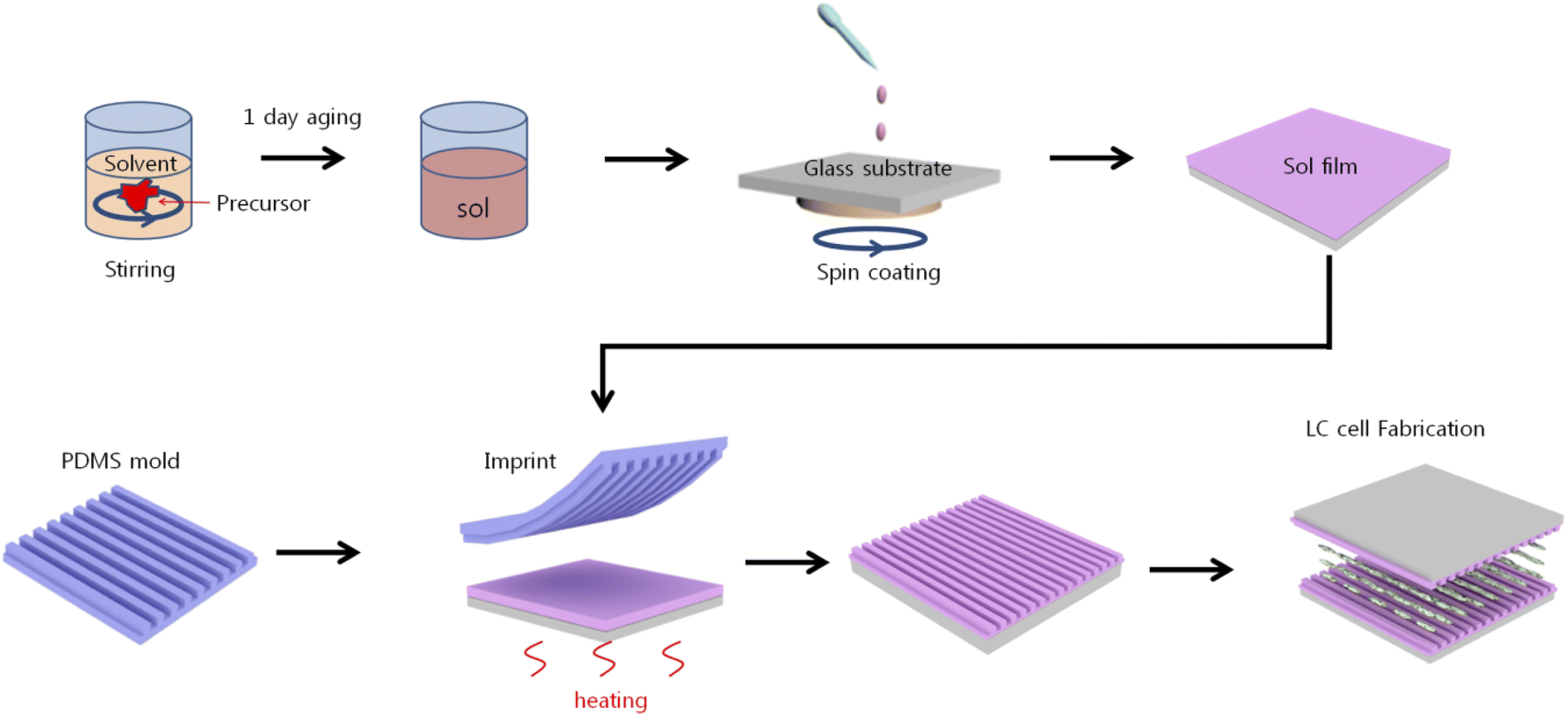
Fig. 1 illustrates the procedures for the LC cell fabrication using nanoimprinting lithography. A polydimethylsiloxane (PDMS) stamp was prepared by mixing an elastomer base and a curing agent (both part of the Sylgard-184 elastomer kit, Dow Corning) at a volume ratio of 10![[thin space (1/6-em)]](https://www.rsc.org/images/entities/char_2009.gif) :1. The mixture was placed into a desiccator equipped with a pump to remove trapped air bubbles. A silicon (Si) mold fabricated using laser interference lithography with a periodicity of 880 nm and a height of 30 nm was used as the master for the nanopatterned structure. The bubble-free PDMS mixture was poured onto the Si mold and cured at 65 °C for 120 min, then peeled off. 0.1 M SnO2 was prepared by dissolving tin(II) chloride (SnCl2) in 2-methoxyethanol (2ME). Mono-ethanolamine (MEA) and acetic acid were added dropwise to obtain a stable and homogeneous SnO solution which was then stirred for 4 h at 65 °C using a magnetic stirrer followed by aging for at least 1 day to obtain a homogeneous sol state of the solution.
:1. The mixture was placed into a desiccator equipped with a pump to remove trapped air bubbles. A silicon (Si) mold fabricated using laser interference lithography with a periodicity of 880 nm and a height of 30 nm was used as the master for the nanopatterned structure. The bubble-free PDMS mixture was poured onto the Si mold and cured at 65 °C for 120 min, then peeled off. 0.1 M SnO2 was prepared by dissolving tin(II) chloride (SnCl2) in 2-methoxyethanol (2ME). Mono-ethanolamine (MEA) and acetic acid were added dropwise to obtain a stable and homogeneous SnO solution which was then stirred for 4 h at 65 °C using a magnetic stirrer followed by aging for at least 1 day to obtain a homogeneous sol state of the solution.
 | ||
| Fig. 1 A schematic of the fabrication of the LC cell based on the nanopatterned SnO using imprinting lithography. | ||
Indium tin oxide (ITO)-coated glass substrates were ultrasonically cleaned with acetone, methanol, and deionized water for 10 min each and then dried with N2 gas. The prepared SnO solution was spin-coated onto an ITO-coated glass substrate at a spin rate of 3000 rpm for 30 s. The nanopatterned PDMS stamp was placed onto an SnO film at a curing temperature of 100, 150, 200, or 250 °C, thereby transferring the nanostructures onto the SnO film substrate. The obtained nanopatterned SnO substrates were used as alignment layers in LC cells fabricated in an anti-parallel configuration with a cell gap of 60 μm for observing the alignment property. In order to analyze the electro-optical characteristics, a cell was fabricated in TN mode with 5 μm. In the TN mode, positive LCs (IAN-5000XX T14, JNC Co.; ne = 1.595, no = 1.484, Δn = 0.111, Δε = 10.3, Tc = 81.8 °C) were injected by capillary force.
The LC alignment states were observed using polarized optical microscopy (POM; BXP 51, Olympus), and a crystal rotation method (TBA 107, Autronic) was used to measure the pre-tilt angles of the LC molecules on the nanopatterned alignment layer. Transmittance vs. applied voltage graph was measured using LCD evaluation system (LCMS-200. Sesim photonics technology). The surface morphologies of the nanopatterned PDMS stamp and SnO were observed using atomic force microscopy (AFM; Park Systems, XE-BIO) with a scan size of 30 × 30 μm2. The chemical composition of SnO film was analyzed by employing X-ray photoelectron spectroscopy (XPS; Thermo VG, K-alpha) with the calibration of the C 1s peak at 284.4 eV. Optical transmittance was measured using the accumulation mode for three times in the range 250–900 nm at room temperature using an ultraviolet-visible (UV-vis) spectrophotometer (V-650, JASCO Corporation), and the contact angle (CA) was measured using a Phoenix 300 surface angle analyzer (SEO).
Results and discussion
The AFM images presented in Fig. 2 show the morphologies of the nanopatterned PDMS stamp and SnO imprinted with the PDMS stamp according to curing temperature. A high annealing temperature was required to construct or transfer the 3D nanostructures onto the SnO film because the latter was densified and solidified by the heating process. During the imprinting process, the nanopatterned PDMS was placed onto the as-deposited sol film and heat was then applied to the sample concurrently. Underneath, the liquid sol rose and filled in the nanopattern by capillary pressure, which was then solidified by the heat. Subsequently, the nanopattern on the PDMS stamp was transferred to the SnO film.19,20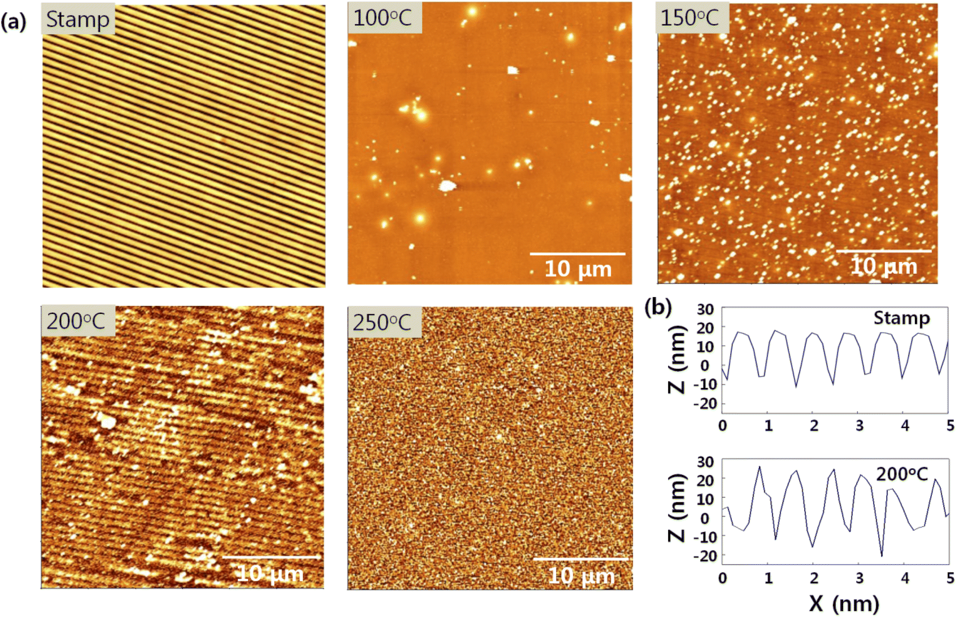 | ||
| Fig. 2 (a) AFM images of the nanostructures created by imprinting lithography according to the annealing temperature, (b) cross-sectional profiles of the nanopatterned PDMS mold and the SnO film imprinted via the PDMS mold. | ||
The nanostructures were observed on the SnO film at a curing temperature of 200 °C but were not transferred at the other curing temperatures. Thus, the nanopattern was successfully transferred to the SnO film at a specific curing temperature of 200 °C, with an average pitch and height of 880 and 30 nm, respectively, which was identical to the nanopattern on the PDMS stamp (Fig. 2(b)). However, below 200 °C was not sufficient for densifying and transferring the nanostructures to the SnO film. In addition, the nanostructures could not be transferred onto the SnO film at curing temperature of 250 °C even with a sufficient heat supply because subjecting the solution-processed oxide material to this temperature led to drastic weight loss by dehydration and decomposition.21–23 Moreover, above 300 °C, we could not detach the PDMS stamp placed onto the SnO film due to the poor thermal stability of the former. PDMS consists of Si–Si linkage in the polymer backbone, and the Si–Si bonds have low bonding energy of 222 kJ mol−1 that can easily undergo homolytic cleavage, thereby causing weight loss at around 300 °C.24
The formation of an SnO thin film prepared by a sol–gel method is dependent on the curing temperature and remains a solvent at a low curing temperature, which hinders the stoichiometric formation, as can be confirmed by its chemical composition.25 The nanopatterned SnO film can be affected by any variation in chemical composition according to the curing temperature. To confirm the chemical composition of the SnO films prepared at 100 and 200 °C, an XPS analysis was conducted, the results of which are shown in Fig. 3. The XPS survey scans were recorded in the range of 0 to 1200 eV (Fig. 3). The Cl 2p, C 1s, Sn 3d, O 1s, and Sn 3p peaks were observed for both SnO film samples, and the survey results confirmed that the SnO film had successfully formed. In addition, distinctly high Sn 3d and Sn 3p peaks were observed from the SnO film cured at 200 °C compared to the one at 100 °C even though similar heights in their O 1s peaks were observed. Additionally, Cl 2p and C 1s peaks were observed from both samples, which arose from the SnCl2 precursor and 2ME, respectively. However, at 200 °C, the Cl 2p and C 1s peaks were very low compared with those of Sn 3p and Sn 3p, which indicates that the SnO film was well-formed at 200 °C rather than at 100 °C, and was closer to the stoichiometric composition.
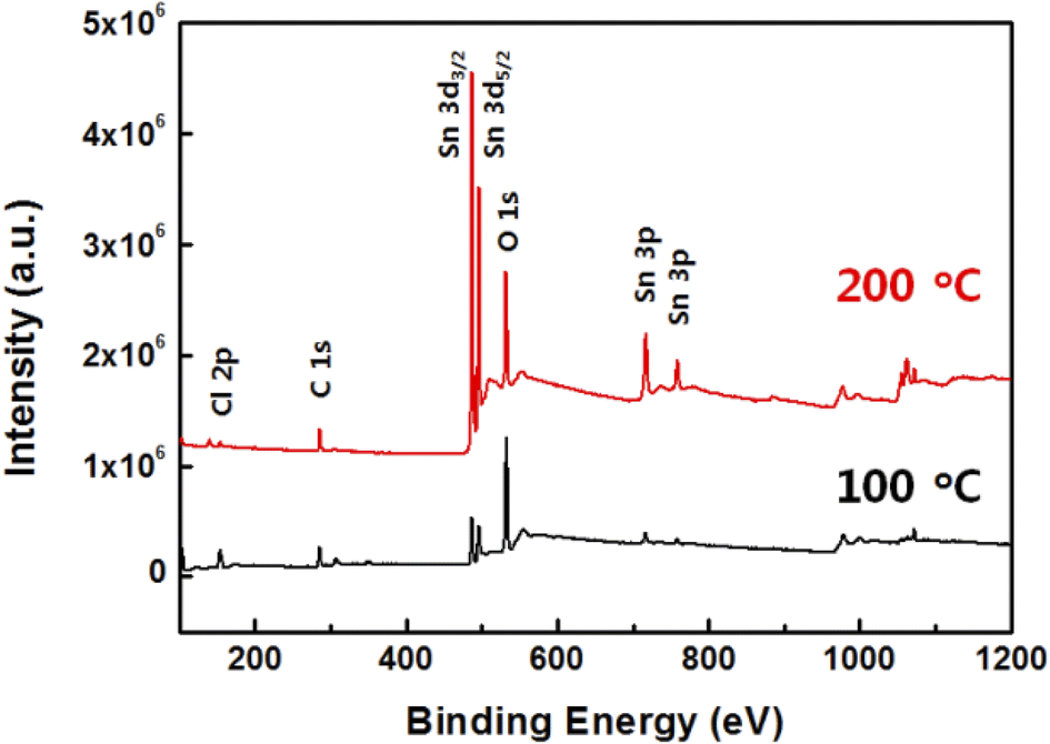 | ||
| Fig. 3 A wide-survey XPS spectrum in the range of 0 to 1200 eV. | ||
In detail, the high-resolution XPS spectra of C 1s, Sn 3d, O 1s, and the corresponding peaks were analyzed at curing temperatures of 100 and 200 °C (Fig. 4). The high-resolution C 1s spectra showed different shapes according to the curing temperature. The C 1s spectrum for the SnO film at 100 °C comprised a major peak at 284.4 eV (C–C bonds) and two smaller peaks at 285.6 (C–O bonds) and 288.8 (C![[double bond, length as m-dash]](https://www.rsc.org/images/entities/char_e001.gif) O bonds), whereas the C 1s spectrum for was composed of a major peak at 284.4 (C–C bonds), and two smaller peaks at 286.5 (C–O bonds), and 288.8 eV (CO bonds). Note that the sub-peak for the C–O bonds in the SnO film cured at 200 °C showed a right shift of 0.9 eV at 200 °C, which could be attributed to the formation of C–O–M (M = metal, i.e. Sn in this study). The O 1s spectra were deconvoluted into two peaks centered at 530.7 and 532.0 eV: the one at 530.7 eV was assigned to the Sn–O bonds and the one at 532.0 eV resulted from the oxygen deficiency inside of the Sn–O matrix. A large number of oxygen vacancies rather than Sn–O bonds was the result of the low curing temperature. With the curing temperature at 200 °C, the Sn–O bonds increased but the oxygen vacancies were reduced because oxygen atoms filled the oxygen vacancies at the higher curing temperature; the reduction in oxygen vacancies was accompanied by the stable formation of Sn–O bonds in the SnO film. The Sn 3d spectrum was in the range from 484 to 500 eV. Due to the spin–orbit splitting, the doublet peaks Sn 3d5/2 and Sn 3d3/2 appeared at 486.9 and 495.3 eV, respectively, and the spin–orbit splitting peaks were separated by 8.4 eV, which is in agreement with previously reported data;26 the Sn 3d peaks corresponded to Sn 4+ ions.27 A peak at 496.9 eV is evident at a curing temperature of 100 °C, which is related to the Sn–Cl bonds due to the SnCl2 dihydrate precursor. The results indicate that the Sn atoms were in a well-oxidized state at a curing temperature of 200 °C.
O bonds), whereas the C 1s spectrum for was composed of a major peak at 284.4 (C–C bonds), and two smaller peaks at 286.5 (C–O bonds), and 288.8 eV (CO bonds). Note that the sub-peak for the C–O bonds in the SnO film cured at 200 °C showed a right shift of 0.9 eV at 200 °C, which could be attributed to the formation of C–O–M (M = metal, i.e. Sn in this study). The O 1s spectra were deconvoluted into two peaks centered at 530.7 and 532.0 eV: the one at 530.7 eV was assigned to the Sn–O bonds and the one at 532.0 eV resulted from the oxygen deficiency inside of the Sn–O matrix. A large number of oxygen vacancies rather than Sn–O bonds was the result of the low curing temperature. With the curing temperature at 200 °C, the Sn–O bonds increased but the oxygen vacancies were reduced because oxygen atoms filled the oxygen vacancies at the higher curing temperature; the reduction in oxygen vacancies was accompanied by the stable formation of Sn–O bonds in the SnO film. The Sn 3d spectrum was in the range from 484 to 500 eV. Due to the spin–orbit splitting, the doublet peaks Sn 3d5/2 and Sn 3d3/2 appeared at 486.9 and 495.3 eV, respectively, and the spin–orbit splitting peaks were separated by 8.4 eV, which is in agreement with previously reported data;26 the Sn 3d peaks corresponded to Sn 4+ ions.27 A peak at 496.9 eV is evident at a curing temperature of 100 °C, which is related to the Sn–Cl bonds due to the SnCl2 dihydrate precursor. The results indicate that the Sn atoms were in a well-oxidized state at a curing temperature of 200 °C.
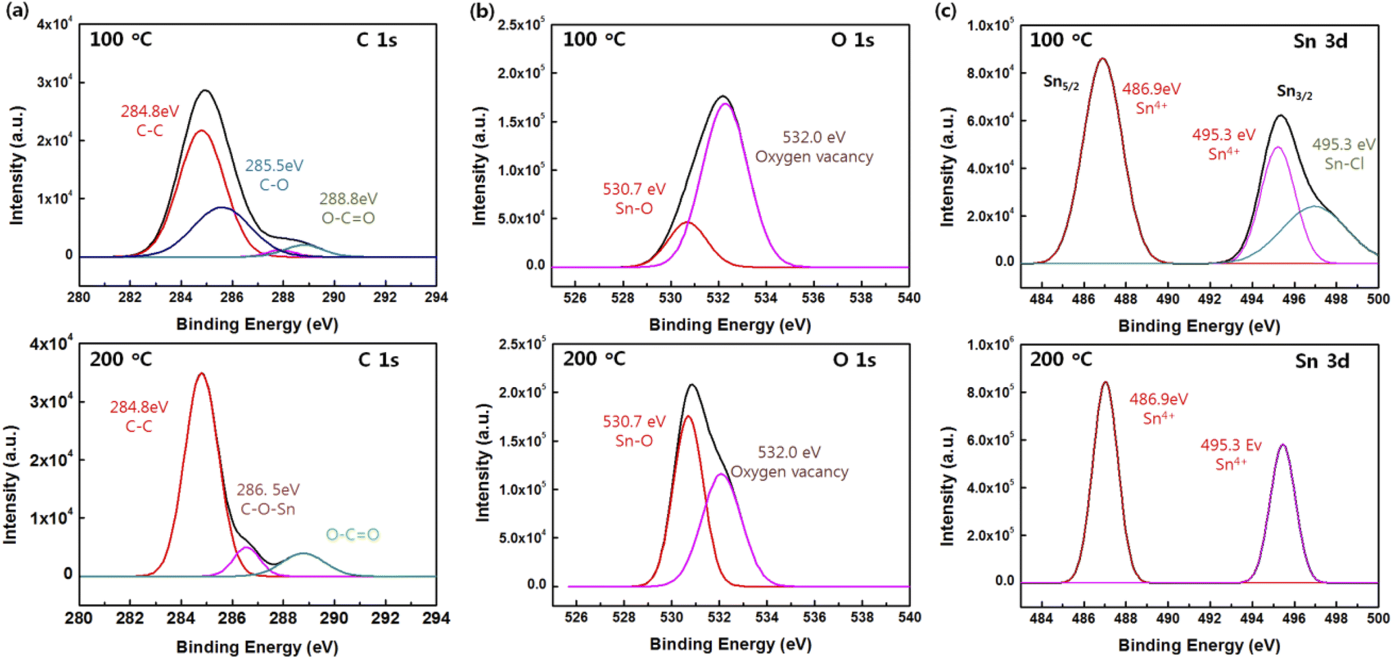 | ||
| Fig. 4 High-resolution (a) C 1s, (b) O 1s, and (c) Sn 3d XPS spectra of the SnO films cured at 100 and 200 °C. | ||
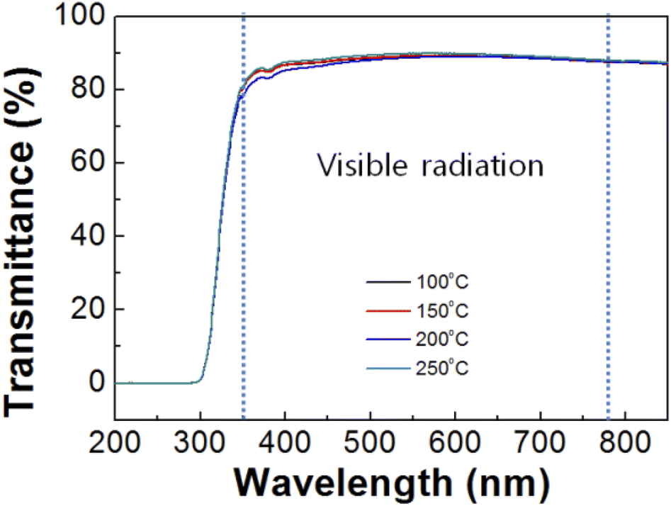
Fig. 5 shows UV-vis transmittance spectra of the SnO films after imprinting according to annealing temperature. In the visible region (350 to 780 nm), the average transmittances of the SnO films at annealing temperatures of 100, 150, 200, and 250 °C were 87.9, 88, 87.4, and 88.5%, respectively. At an annealing temperature of 200 °C, the transmittance was reduced compared to the other temperatures, which could have been the effect of the 3D nanostructures due to light scattering or light trapping in waveguide mode.28,29 Thus, a decrease in transparency resulted from the nanostructures in the SnO film.
 | ||
| Fig. 5 UV-vis transmittance spectra of the SnO imprinted via the PDMS mold at different annealing temperatures. | ||
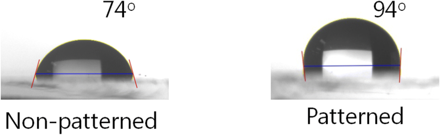
Fig. 6 shows the CA measurements on the non-patterned and patterned surfaces. It is known that surface wettability depends on the topological characteristics, thus the nanopatterned SnO film had a higher water CA compared to the non-patterned film, measured as 94° and 74°, respectively. This indicates that the non-patterned film showed hydrophilicity whereas the patterned surface was hydrophobic. When the droplets lay down on the patterned surface, the water could not permeate the grooves, and thus an air trap between the droplet and the patterned surface was created.30 Because this led to a composite solid–liquid–air interface, the water CA of the patterned surface was higher than that of the non-patterned surface. From these results, we can confirm that the nanopatterned structure was well transferred to the SnO film from the nanopatterned PDMS stamp.
 | ||
| Fig. 6 Contact-angle measurements of the non-patterned and patterned SnO films. | ||
Fig. 7(a) presents POM images of the LC cells based on the nanopatterned SnO film as an alignment layer according to curing temperature; these were used to evaluate the alignment properties of the LC cell. Uniform alignment characterized by a black image under crossed polarizers was observed at the curing temperature of 200 °C, which indicates that the LC molecules were unidirectionally aligned along the direction of the nanopattern on the SnO film. Because the LCs were made of a birefringent material, well-aligned LCs along one direction of the intersectional polarizer blocked light penetration from the bottom. However, except at a curing temperature of 200 °C, locally different transmittances were observed in the POM images, resulting from the randomly aligned LC molecules in the LC cell. Transmittance oscillation was measured by projecting a light beam on rotating LC cells, the results of are shown in Fig. 7(b). The blue curve represents the simulated data and the red curve the data measured from the LC cells. Graphs were drawn to demonstrate how well the LC molecules had been uniformly aligned in the alignment layer. If the red curve coincided with the blue curve, the pre-tilt angle of the LCs on alignment layer was accurately estimated, and this would indicate that the LC molecules were uniformly aligned on the alignment layer with a stable pre-tilt angle. However, the difference between the simulated and the measured curves indicated the random alignment state of the LC molecules because without being in the preferred direction, they were not able to control the transmittance. At a curing temperature of 200 °C, the LC molecules were uniformly aligned and the calculated pre-tilt angle was measured as 0.5° on average. In contrast, there were large differences between the simulated and experimental curves at a curing temperature of 250 °C due to the random alignment state of the LC molecules, thus the pre-tilt angle could not be determined.
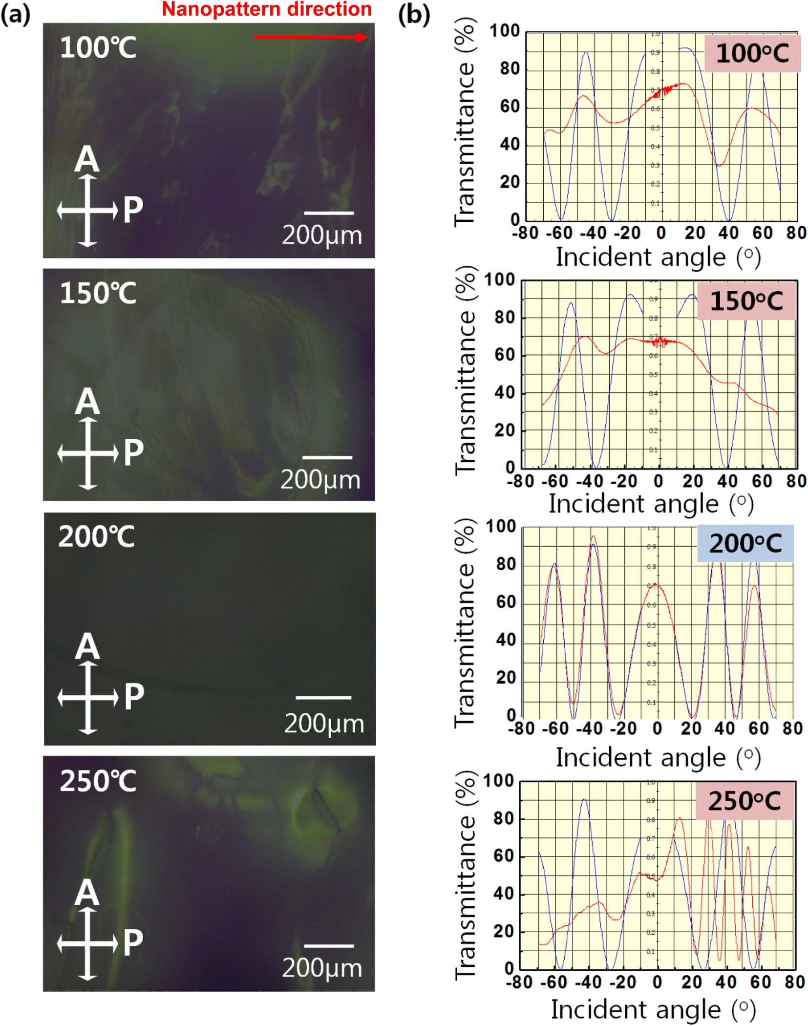 | ||
| Fig. 7 (a) POM images of the LC cell based on the SnO imprinted via the PDMS mold at different annealing temperatures, and (b) transmittances of the LC cell measured under latitudinal rotation. | ||
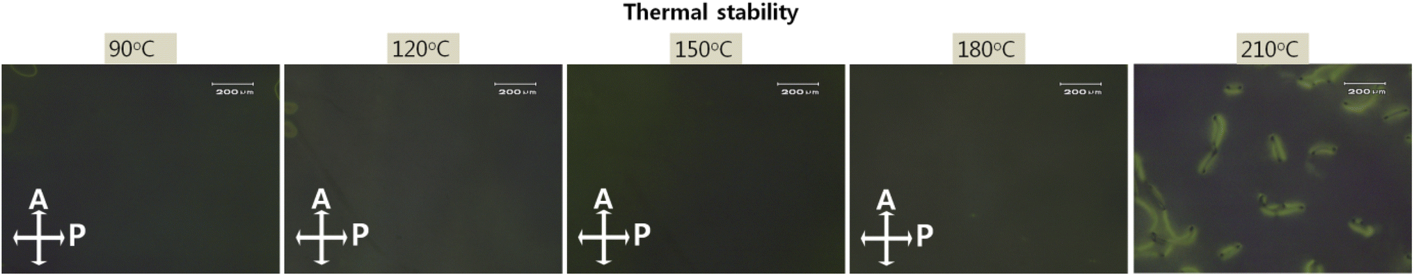
The demand for high-resolution and high brightness in advanced LC applications requires high thermal stability. The increased integrated circuit and high power consumption generate heat, thereby inducing thermal deterioration by LC alignment. Fig. 8 exhibits photomicrographs of LC cells based on the nanopatterned SnO films obtained by annealing at temperatures from 90 to 210 °C for 10 min, all of which attained good thermal stability. Stable homogeneous alignment of the LC molecules was preserved until 180 °C, with higher endurance than conventional rubbed PI at 150 °C. The ordered nanopattern was able to strongly anchor the LC molecules in the same direction, which indicates that the LC molecules on the nanopatterned SnO film had a high thermal budget, thus making it an appropriate candidate for advanced LC applications.
 | ||
| Fig. 8 POM images of LC cell based on the nanopatterned SnO heated to temperatures of 90–210 °C. | ||
Fig. 9 shows the electro-optical characteristics of TN mode LC cells based on the nano-patterned SnO at annealing temperature of 200 °C and LC cells based on the rubbed PI. In Fig. 9(a) and (b), graphs of response time and relative transmittance are expressed by dividing rise time and fall time, respectively. In Fig. 9(a), the rise time of rubbed PI was 2.4 ms and that of nanopatterned SnO was 6.7 ms. In Fig. 9(b), the fall time of rubbed PI was 12.1 ms and that of nanopatterned SnO was 11.3 ms.31 Fig. 9(c) shows the graph of the V–T curve of each sample. The threshold voltage (Vth) was 1.49 V for rubbed PI and 1.45 V for nanopatterned SnO. In conclusion, in the electro-optical properties of the nanopatterned SnO cell, other properties except for the rise time showed similar levels to those of rubbed PI.
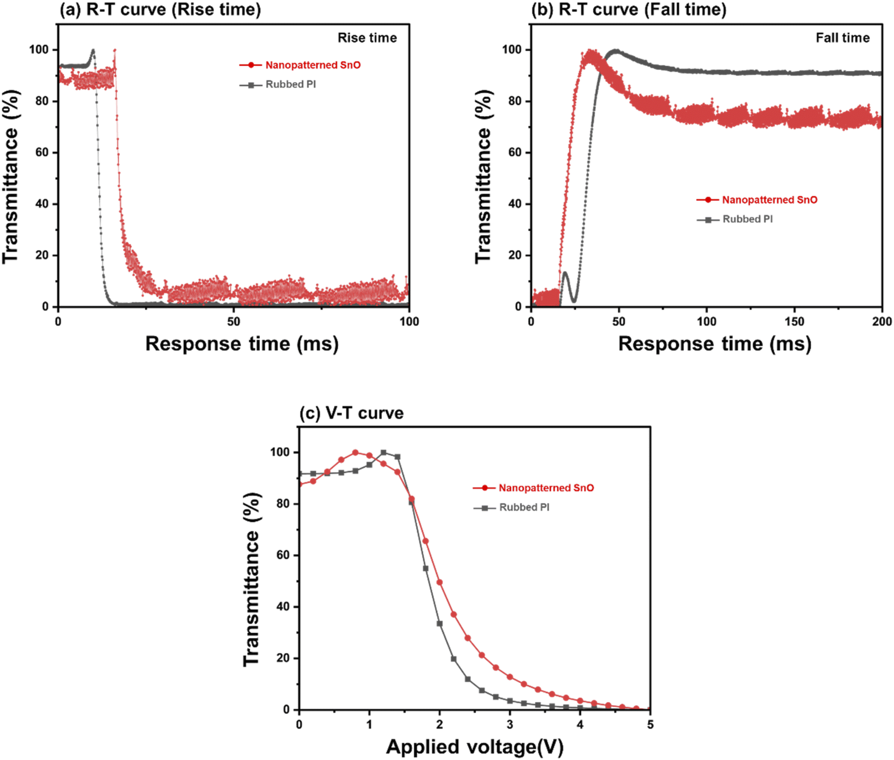 | ||
| Fig. 9 (a) R–T curves characteristics (rise time) of the TN-LC cells on the nano patterned SnO and rubbed PI, (b) R–T curves characteristics (fall time) of the TN-LC cells on the nano patterned SnO and rubbed PI, (c) V–T curves characteristics of the TN-LC cells on the nano patterned SnO and rubbed PI. | ||
In Fig. 10, the polar anchoring energy of the nanopatterned SnO LC cell was measured, and the value of 2.02 × 10⁻⁴ J m−2 was confirmed. Considering that the anchoring energy value of rubbed PI, which is generally used, is about 10−3 J m−2, and the anchoring energy value of photoalignment and SiO oblique deposition, which are studied as alternative methods of the rubbing method, is formed at about 10−5 J m−2, the anchoring energy values of nanopatterned SnO can be considered to be satisfactory.
 | ||
| Fig. 10 Anchoring energy characteristic of the LC cell assembled by nanopatterned SnO films cured at 200 °C. | ||
Conclusion
We demonstrated nanoimprinting lithography on solution-processed SnO film for use as an LC alignment layer, which is a very convenient and cost-effective method for aligning LCs. The imprinted nanostructures on the solution-processed SnO film could be transferred using a nanopatterned PDMS stamp at a curing temperature of 200 °C. The obtained nanostructures on the SnO film acted as a guide for the arrangement of the LC molecules and induced geometric restriction, which minimized elastic distortion energies, thereby leading to alignment in the direction of the nanostructure. With a high thermal endurance of 180 °C and drastically low power consumption of the threshold voltage of 2.124 V for VA mode, the nano patterned SnO film was shown to be a promising candidate material for LC applications. Nanoimprinting lithography combined with solution-processed inorganic materials exhibited the possibility of broadening the features of nanostructure-mounted applications, including LC devices.Conflicts of interest
The authors declare no competing financial interest.Acknowledgements
This research was supported by the National Research Foundation of Korea (Grant No. 2020R1G1A1013604).References
- M. F. Toney, T. P. Russell, J. A. Logan, H. Kikuchi, J. M. Sands and S. K. Kumar, Nature, 1995, 374, 709–711 CrossRef CAS.
- P. Chaudhari, J. Lacey, J. Doyle, E. Galligan, S. C. A. Lien, A. Callegari, G. Hougham, N. D. Lang, P. S. Andry, R. John, K. H. Yang, M. Lu, C. Cai, J. Speidell, S. Purushothaman, J. Ritsko, M. Samant, J. Stöhr, Y. Nakagawa, Y. Katoh, Y. Saitoh, K. Sakai, H. Satoh, S. Odahara, H. Nakano, J. Nakagaki and Y. Shiota, Nature, 2001, 411, 56–59 CrossRef CAS PubMed.
- J. Stöhr, M. G. Samant, J. Lüning, A. C. Callegari, P. Chaudhari, J. P. Doyle, J. A. Lacey, S. A. Lien, S. Purushothaman and J. L. Speidell, Science, 2001, 292, 2299–2302 CrossRef PubMed.
- P. K. Son, J. H. Park, S. S. Cha, J. C. Kim, T. H. Yoon, S. J. Rho, B. K. Jeon, J. S. Kim, S. K. Lim and K. H. Kim, Appl. Phys. Lett., 2006, 88, 2–5 CrossRef.
- Y. G. Kang, H. J. Kim, H. G. Park, B. Y. Kim and D. S. Seo, J. Mater. Chem., 2012, 22, 15969–15975 RSC.
- P. J. Shannon, W. M. Gibbons and S. T. Sun, Nature, 1994, 368, 532–533 CrossRef CAS.
- M. Schadt, H. Seiberle, A. Schuster and S. M. Kelly, Jpn. J. Appl. Phys., 1995, 34, L764–L767 CrossRef CAS.
- M. Schadt, K. Schmitt, V. Kozinkov and V. Chigrinov, Jpn. J. Appl. Phys., 1992, 31, 2155–2164 CrossRef CAS.
- H. G. Park, J. J. Lee, K. Y. Dong, B. Y. Oh, Y. H. Kim, H. Y. Jeong, B. K. Ju and D. S. Seo, Soft Matter, 2011, 7, 5610–5614 RSC.
- J. C. Armas-Pérez, X. Li, J. A. Martínez-González, C. Smith, J. P. Hernández-Ortiz, P. F. Nealey and J. J. De Pablo, Langmuir, 2017, 33, 12516–12524 CrossRef.
- M. Jenik, A. Seifner, S. Krassnig, K. Seidler, P. A. Lieberzeit, F. L. Dickert and C. Jungbauer, Biosens. Bioelectron., 2009, 25, 9–14 CrossRef CAS PubMed.
- S. W. Ahn, K. D. Lee, J. S. Kim, S. H. Kim, J. D. Park, S. H. Lee and P.-W. Yoon, Nanotechnology, 2005, 16, 1874–1877 CrossRef CAS.
- P. M. Mendes, S. Jacke, K. Critchley, J. Plaza, Y. Chen, K. Nikitin, R. E. Palmer, J. A. Preece, S. D. Evans and D. Fitzmaurice, Langmuir, 2004, 20, 3766–3768 CrossRef CAS.
- M. Erdmanis, P. Sievilä, A. Shah, N. Chekurov, V. Ovchinnikov and I. Tittonen, Nanotechnology, 2014, 25, 335302 CrossRef CAS PubMed.
- H. C. Jeong, G. S. Heo, E. M. Kim, H. G. Park, J. H. Lee, J. M. Han and D. S. Seo, J. Sol-Gel Sci. Technol., 2016, 79, 29–36 CrossRef CAS.
- J. H. Lee, H. C. Jeong, H. G. Park and D. S. Seo, RSC Adv., 2015, 5, 54079–54084 RSC.
- H. C. Jeong, B. Y. Oh, H. G. Park, J. H. Lee, Y. H. Jung, S. B. Jang and D. S. Seo, Opt. Mater., 2015, 50, 104–109 CrossRef CAS.
- H. G. Park, H. C. Jeong, J. J. Han, S. Y. Kim, J. H. Kim, D. H. Kim and D.-S. Seo, J. Mater. Chem., 2014, 2, 3960–3964 CAS.
- S. Sarkar, R. Chattopadhyay and S. Jana, RSC Adv., 2016, 6, 109218–109233 RSC.
- K. Y. Suh, M. C. Park and P. Kim, Adv. Funct. Mater., 2009, 19, 2699–2712 CrossRef CAS.
- S. Y. Kim, H. G. Park, M. J. Cho, H. C. Jeong and D. S. Seo, Liq. Cryst., 2014, 41, 940–945 CrossRef CAS.
- H. Zhang, H. Ke, P. Ying, H. Luo, L. Zhang, W. Wang, D. Jia and Y. Zhou, J. Sol-Gel Sci. Technol., 2018, 85, 132–139 CrossRef CAS.
- G. N. Shao, S. M. Imran, S. J. Jeon, S. J. Kang, S. M. Haider and H. T. Kim, Appl. Surf. Sci., 2015, 351, 1213–1223 CrossRef CAS.
- Y. Meng, J. Xue, J. Chu, C. Liu, Z. Wang and L. Zhang, RSC Adv., 2014, 4, 31249–31260 RSC.
- H. C. Jeong, G. S. Heo, E. M. Kim, J. H. Lee, J. M. Han and D. S. Seo, Opt. Mater., 2017, 64, 569–573 CrossRef CAS.
- R. Al-Gaashani, S. Radiman, N. Tabet and A. R. Daud, Mater. Sci. Eng., B, 2012, 177, 462–470 CrossRef CAS.
- D. J. Yang, I. Kamienchick, D. Y. Youn, A. Rothschild and I. D. Kim, Adv. Funct. Mater., 2010, 20, 4258–4264 CrossRef CAS.
- M. C. Van Lare and A. Polman, ACS Photonics, 2015, 2, 822–831 CrossRef CAS.
- M. L. Brongersma, Y. Cui and S. Fan, Nat. Mater., 2014, 13, 451–460 CrossRef CAS PubMed.
- D. Vollmer and H.-J. Butt, Nature, 2015, 527, 41–42 CrossRef CAS PubMed.
- H. G. Park, H. Y. Mun, H. C. Jeong, B. Y. Oh, J. M. Han and D. S. Seo, Soft Mater., 2018, 16, 71–76 CrossRef CAS.
| This journal is © The Royal Society of Chemistry 2022 |