DOI:
10.1039/D2RA04438B
(Paper)
RSC Adv., 2022,
12, 25570-25577
Metal halide perovskite layers studied by scanning transmission X-ray microscopy†
Received
18th July 2022
, Accepted 8th August 2022
First published on 8th September 2022
Abstract
We describe the investigation of metal halide perovskite layers, particularly CH3NH3PbI3 used in photovoltaic applications, by soft X-ray scanning transmission X-ray microscopy (STXM). Relevant reference spectra were used to fit the experimental data using singular value decomposition. The distribution of key elements Pb, I, and O was determined throughout the layer stack of two samples prepared by wet process. One sample was chosen to undergo electrical biasing. Spectral data shows the ability of STXM to provide relevant chemical information for these samples. We found the results to be in good agreement with the sample history, both regarding the deposition sequence and the degradation of the perovskite material.
1 Introduction
Research on hybrid organic-inorganic metal halide perovskite (MHP) semiconductors saw a steep rise due to their breakthrough application in the field of photovoltaic (PV) technologies. One decade after the first ever report of their use in PV devices,1 they are now directly challenging the most prominent actor in the field and current market leader: crystalline silicon (c-Si).2 Among their numerous advantages are the wide degree of freedom in chemical composition, which enables a wide tuneable range of optoelectronic properties, and low-cost synthesis. Despite the apparent simplicity of deriving high-quality MHP thin-films and their recently attained widespread use in research laboratories, halide perovskites define a material class with a unique combination of properties and have, as such, not been investigated to their full extent. The research community is no longer solely focusing on the photovoltaic efficiency race, which was driving the advancement of research over the past years. Interest has now turned towards increasing their stability and reliability, notably by chemical composition tuning3,4 and the study of structure–property relationships. As perovskite depicts the currently most promising material for reliable high efficiency solar cells, a deeper understanding of key properties, such as charge carrier lifetime, defect physics, mobility, degradation mechanism, or phase segregation, is needed. First, on the stand-alone level, but even more so when the material is integrated into more complex structures and device architecture, interfaces to other materials are involved and impose additional external parameters on the MHP chemical and physical properties.5 The latter is particularly important for the design of the next generation of halide-perovskite-based optoelectronic devices, for which the selection of charge selective extraction layers requires a dedicated chemical analysis at the interface.6 In addition to this, ion migration through crystallographic point defects is one of the phenomena that is in part responsible for a wider range of interesting features in these material, such as current–voltage hysteresis,7–9 the light soaking effect,10–12 photo-induced ion segregation,13,14 etc. The ability to probe the deviation from the ideal stoichiometry in these devices can possibly improve our understanding of stability, defect concentrations, and ion migration pathways. Besides the relatively straight-forward and easily available characterisation techniques of scanning electron microscopy (SEM), X-ray diffraction (XRD)15,16 or UV-visible absorption spectroscopy,17 perovskite layers have also been studied using more exotic and complex techniques such as high angle annular dark-field scanning transmission electron microscopy (HAADF-STEM),18 time-of-flight secondary ion mass spectrometry (TOF-SIMS),19 glow-discharge optical emission spectroscopy (GD-OES),20 ultraviolet, X-ray and inverse photoemission spectroscopy (UPX, XPS, IPES),21 various X-ray microscopy techniques,22 Kelvin-probe force microscopy (KPFM),23 impedance spectroscopy24 or Space-Charge-Limited Current (SCLC).25 In this paper, we exemplify the use of scanning transmission X-ray microscopy (STXM) to investigate the chemical properties and composition gradients in perovskite films and corresponding solar cell layer stacks.
STXM is a soft X-ray spectromicroscopy technique based on the detection of photons transmitted through the bulk of a raster-scanned sample. The STXM setup consists of a set of optics (a Fresnel Zone Plate (FZP) to focus the beam and an Order Sorting Aperture (OSA) to remove rays of a diffraction order higher than one), a scanning stage where the studied sample is mounted, and a photon detector (Fig. 1a). One of the distinctive features of STXM is that it combines imaging with spectral analysis. This dual-mode analysis makes it a powerful technique to study chemically complex materials with nanoscale inhomogeneities.26 This latter can be explained by its combined features of high spatial resolution and chemical sensitivity. Spatial resolutions below 50 nm are now routinely achieved in STXM setups,27,28 with best-effort resolutions reaching 7 nm.29 Depending upon the beamline, this technique also allows a high spectral resolution with E/dE ∼ 10![[thin space (1/6-em)]](https://www.rsc.org/images/entities/char_2009.gif) 000 in the soft X-ray regime. In this work, we use a Fresnel zone plate with a spatial resolution of ∼40 nm and a spectral resolution at the HERMES beamline in the energy range investigated of ∼ 10000. STXM has been extensively used to study polymer blends.30–40 Organic–inorganic metal halide perovskites are relatively new. Apart from a paper from our group,41 very few reports of STXM studies were found in the literature. In Lin et al.,42 the material formation was investigated following the exposure of PbI2 films to methylammonium iodide and in Li et al.43 the integration of a phenyl ethylammonium cation to the perovskite network was studied. In both cases, the images were acquired in a top view of the samples, i.e., with an X-ray under an angle of incidence normal to the sample plane. The present study in which the perovskite layer is studied in a cross-section configuration (see Fig. 1a), is to our knowledge the first of its kind. The cross-section configuration allows the study of the material in its bulk dimension and its interfaces with adjacent layers. Hence, our study serves as a basis to investigate cross-sections of complex halide perovskite-based device architectures such as halide perovskite solar cells, for which chemical and structural properties at the nanoscale and at the interfaces dominate performance and stability.44 The high spectral and spatial resolution of STXM offers the possibility to assess changes in the material both quantitatively (composition) and qualitatively (morphology).
000 in the soft X-ray regime. In this work, we use a Fresnel zone plate with a spatial resolution of ∼40 nm and a spectral resolution at the HERMES beamline in the energy range investigated of ∼ 10000. STXM has been extensively used to study polymer blends.30–40 Organic–inorganic metal halide perovskites are relatively new. Apart from a paper from our group,41 very few reports of STXM studies were found in the literature. In Lin et al.,42 the material formation was investigated following the exposure of PbI2 films to methylammonium iodide and in Li et al.43 the integration of a phenyl ethylammonium cation to the perovskite network was studied. In both cases, the images were acquired in a top view of the samples, i.e., with an X-ray under an angle of incidence normal to the sample plane. The present study in which the perovskite layer is studied in a cross-section configuration (see Fig. 1a), is to our knowledge the first of its kind. The cross-section configuration allows the study of the material in its bulk dimension and its interfaces with adjacent layers. Hence, our study serves as a basis to investigate cross-sections of complex halide perovskite-based device architectures such as halide perovskite solar cells, for which chemical and structural properties at the nanoscale and at the interfaces dominate performance and stability.44 The high spectral and spatial resolution of STXM offers the possibility to assess changes in the material both quantitatively (composition) and qualitatively (morphology).
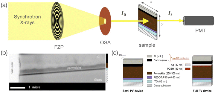 |
| | Fig. 1 (a) Schematic outline of the STXM set up with the Fresnel Zone Plate (FZP) focusing device, the Order Sorting Aperture (OSA) filter, the sample loaded on a [x; y] scanning stage and a photomultiplier (PMT) photon detector; (b) high resolution image at 490 eV of a semi PV device with a dry-processed perovskite layer and (c) stack of semi and full PV device FIB-milled lamella with layer assignation and nominal thickness values (C and Pt layers correspond to pre-FIB protection, their exact thickness is unknown). | |
For the present study, two samples of the reference CH3NH3PbI3 (MAPbI3) perovskite material were investigated: two wet-processed perovskite layers were integrated into a full PV device stack (i.e. glass/ITO/PEDOT:PSS/MAPbI3/phenyl-C61-butyric acid methyl ester (PCBM)/Ag), either used as is (henceforth referred to as unbiased sample) or used after 1 week electrical-biasing (henceforth referred to as biased sample). In each case, we prepared a ∼200 nm thick cross-section lamella by a Focused Ion Beam (FIB) process for further investigation by STXM. More details of the sample preparation from bulk to cross-section lamella are described in the Experimental section.
So far, the use of techniques that employ monochromatic X-rays in the low soft X-ray regime (<1000 eV) for the investigation of halide perovskites has been challenging primarily because of the lack of well-defined X-ray absorption edges for Pb and I in this regime. However, only this spectral regime offers the opportunity to track light elements, particularly carbon, oxygen and nitrogen, which are either important markers for the organic cation in the perovskite samples or part of crucial degradation products. In addition, the possibility to obtain chemical sensitive information at individual elemental edges is also presented. The objective of the present study is (a) to introduce the use of STXM to investigate these hybrid organic inorganic halide perovskite compounds and (b) to investigate and present the changes in chemical composition of wet processed samples under biased and unbiased conditions.
2 Results and discussion
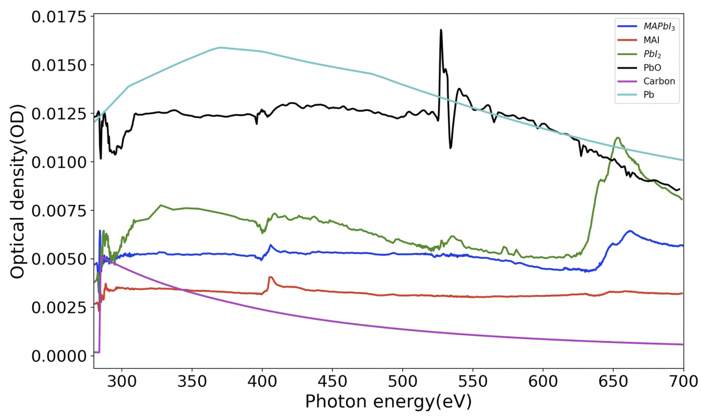
Analysis of STXM data (images and/or spectra) to get quantitative information can be conducted by singular value decomposition (SVD).45 However, in order to use these techniques effectively, it is necessary to obtain reference spectra of samples with their known thickness. Hence we have synthesized and obtained the X-ray absorption spectra (XAS) of thin films of MAPbI3, MAI (methylammonium iodide), PbI2 and PbO. Fig. 2 shows these spectra normalized to 1 nm equivalent thickness. This thickness, conventionally known as OD1 spectrum (elemental optical density spectrum for 1 nm thickness) is the input spectrum for the SVD. The carbon and lead spectra shown in Fig. 2 were simulated.
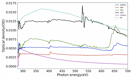 |
| | Fig. 2 Spectra of MAPbI3 and various reference component materials converted to OD1 (1 nm equivalent). The densities used for converting the experimental spectra to OD1 are MAI: 2.28 g cm−3, PbI2: 6.16 g cm−3 and PbO: 9.5 g cm−3. The spectra of carbon and lead were simulated 46 with the densities of C = 2.26 g cm−3 and Pb = 11.3 g cm−3. Raw data for MAI was taken from ref. 42. | |
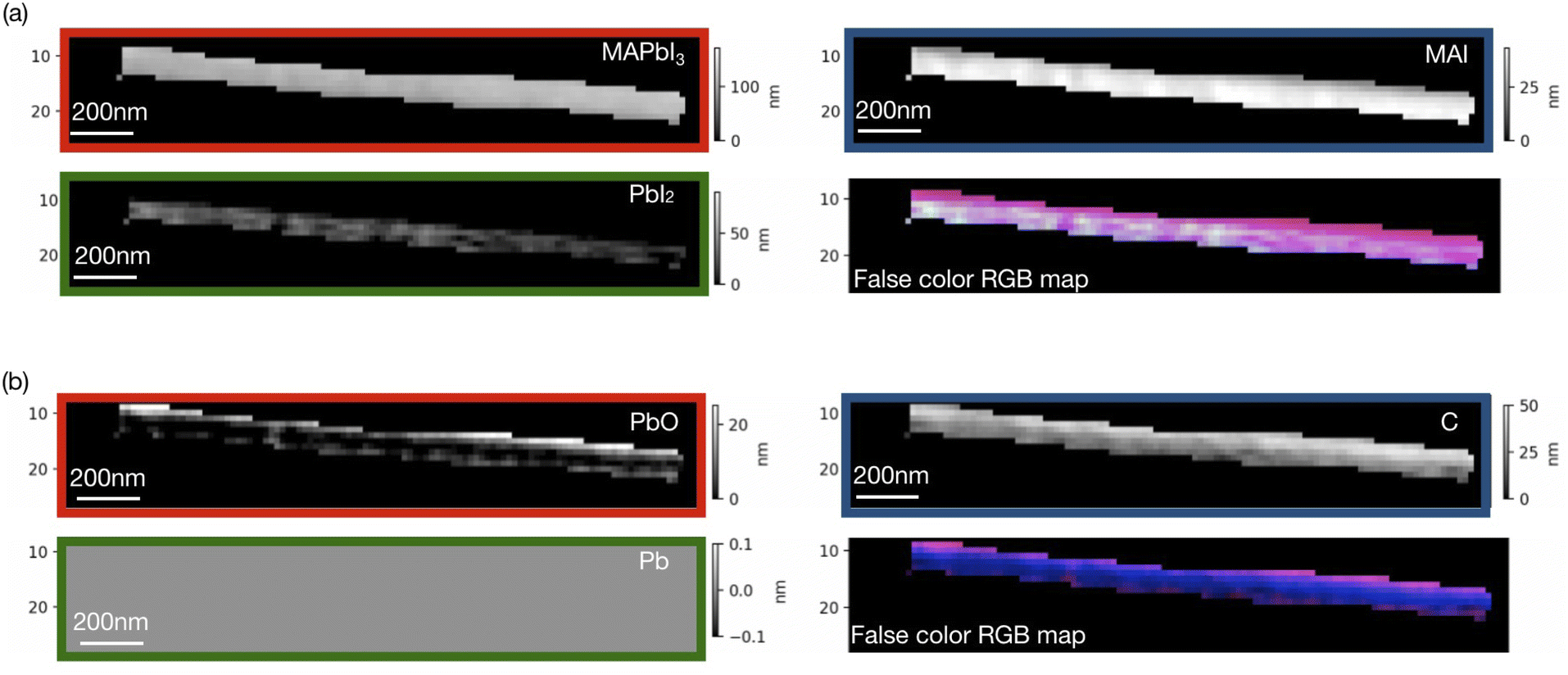
Singular value decomposition was performed using the software aXis2000.46 Fig. 3 and 4 show SVD results (component thickness maps) of the unbiased and biased samples. The Pb/I ratio, O/I ratio, and fitting error maps of the samples are shown in Fig. S1 and S2.†
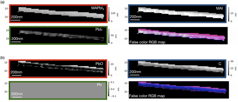 |
| | Fig. 3 Results of SVD of the unbiased sample showing (a) the component maps of the MAPbI3, MAI and PbI2 along with a RGB false color map, and (b) showing the component maps of PbO, C and Pb along with a RGB false color map (scale bar = 200 nm). | |
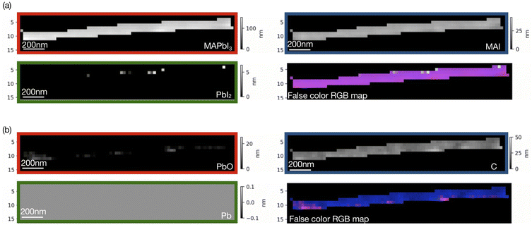 |
| | Fig. 4 Results of SVD of the biased sample showing (a) the component maps of the MAPbI3, MAI and PbI2 along with a RGB false color map, and (b) showing the component maps of PbO, C and Pb along with a RGB false color map (scale bar = 200 nm). | |
According to Fig. 3 and 4, along with MAPbI3 there is a significant presence of all the components in the two films. A comparative histogram plot is presented in Fig. S3 and S4.† We observe a rather homogenous thickness of MAI in both the samples. The presence of a thin PbI2 (∼40 nm) layer is observed in the unbiased sample but this component was completely absent in the case of the biased sample. We also observe the presence of a carbon layer in both the samples with a strongly varying thickness in the case of the unbiased sample (see Fig. S3d†). The decomposition of MAI could be a possible reason along with the possibility of hydrocarbon deposition on the sample during measurements. We would like to note once again that the carbon reference spectrum used in the SVD analysis was a simulated spectrum, which could be one of the reasons why the carbon-based species are overestimated.
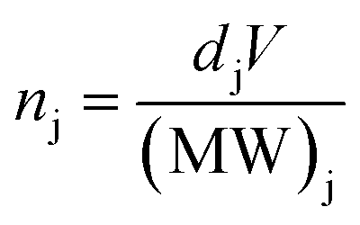
Although the thickness maps allow for convenient visualisation of the relative component distribution, we present in Fig. 5 comparison based on elemental molar concentrations calculated from the results of the SVD fitting. Elemental molar quantities ni (where i is Pb, I, or O) are calculated as the sum of all i-containing j component as expressed in the following set of equations (eqn (1) to (4)):
| | |
nPb = nPb from Pb + nPb from PbO + nPb from PbI2 + nPb from MAPbI3
| (1) |
| | |
nI = 2nI from PbI2 + 3nI from MAPbI3 + nI from MAI
| (2) |
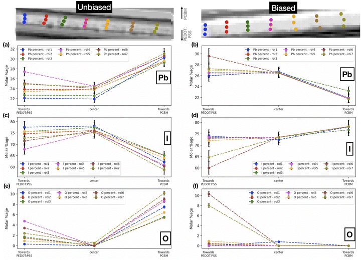 |
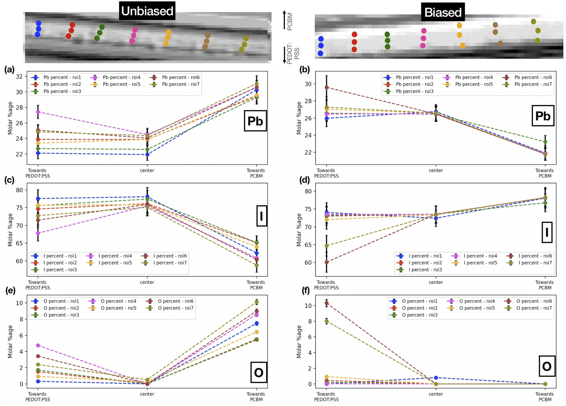
| | Fig. 5 Pb, I and O molar percentages at different points on chosen roi's in the (a, c, e) unbiased and (b, d, f) biased sample. | |
Finally, molar quantities were calculated using the following:
| |
 | (4) |
where
dj is the component density (
dMAPbI3 = 4.5 g cm
−3,
dMAI = 2.28 g cm
−3,
dPbI2 = 6.16 g cm
−3,
dPbO = 9.5 g cm
−3,
dPb = 11.3 g cm
−3,
dC = 2.26 g cm
−3),
V = [π(beam radius in nm)
2(thickness in nm)] is volume occupied by the component (in nm
3) and (MW)
j is the molecular weight of the component j.
Fig. 5 shows the comparative distribution of the calculated Pb, I, and O molar percentages in both samples. In order to track chemical composition across the cross-section (along the biasing direction) of the films, we have chosen seven different regions of interest (roi's) each one vertically arranged with the first point near the PEDOT:PSS layer (towards the anode), the second point in the center, and the third point closer to the PCBM layer (towards the cathode). For the unbiased sample, the iodine content is higher towards the PEDOT:PSS interface. The oxygen content is higher toward the interface with PCBM in the unbiased as well as the biased sample (albeit less varied). It is noteworthy that these results are also in accordance with the steps in synthesis. It is probable that towards PCBM (i.e., the top of the FIB-milled lamella), the oxygen content is higher given that the top of the lamella is thinner (due to the geometrical set-up of the FIB process). Thus a larger relative fraction of the lamella volume in this region is oxygenated. At the same time, the top interface is rougher with more cavities for the incorporation of oxygen containing species. We further attribute the observed variations in the iodine content, which is higher toward the bottom interface than towards the top interface, to degradation processes in the unbiased sample. Iodine, being a reactive and volatile component in the perovskite composition, remains preserved at the bottom interface, while degradation of the perovskite into its byproducts at the oxygenated top interface is associated with a loss of iodine. Upon biasing, above-discussed trend is suppressed, even reversed to some degree in the case of iodine. Considering that the sample was reverse biased, the iodine ions migrate towards the negative electrode (towards PCBM). We interpret this from the fact that iodine content is much more varied across the perovskite layer as compared to the unbiased sample, underlining the diffusion of iodine ions. On the other hand, oxygen content follows a similar trend as the unbiased sample. We note that this effect of ion migration in halide perovskites can generally be mitigated by halide alloying in the perovskite composition,47 the use of additives in the precursor solutions,48 and surface treatments of the perovskite films, e.g. with excess iodine or electron donating ligands.49 Following our reference measurements performed here, we suggest to compare the impact of iodine migration in these adapted sample systems for future experiments.
Further, the stoichiometry, in terms of Pb/I ratio, is presented in Fig. 6. This measure of stoichiometry, as well as the presented distribution, can provide an indication of the extent and distribution of the degradation process. While variations in elemental composition can be observed in both the samples (Fig. 3 and 4), the overall Pb/I ratio remains less than 0.6. The perovskite stoichiometry implies this ratio to be 0.3, but the values observed in Fig. 6 take into account all the components and by-products. Fig. S4† shows the distribution of these values in both the samples. In order to probe the chemistry further, the individual elemental spectrum at the nitrogen K-edge and iodine M-edge has been extracted from the energy stacks and presented in Fig. 7 for biased and unbiased samples. These spectra are averaged over several randomly chosen pixels and edge-normalized after removing a linear background. The nitrogen K-edge shows several features that present relative variation in intensity. In addition, it is important to note that there are no energy shifts between the two spectra. Feature A (398.5 eV) and B (404 eV) correspond to transitions to bound states.50 The pre-edge feature A is an indication of a degradation product and corresponds to N 1s → π* transitions, while the main peak B has a Rydberg character.50 Feature C (413.1 eV) corresponds to the Pb N5 edge (Pb 4d → 6p*).51 While these features are similar in both spectra, the relative intensity between features B and C is different. The higher difference in intensity between feature B and feature C in the biased sample indicates that in the set of pixels from where the spectra have been extracted, the relative content of saturated N bonds is small compared to the number of Pb atoms. The iodine M-edge spectra exhibit two remarkable features and are similar for the biased and unbiased samples. The difference in the normalized spectra directly relates to the iodine content in the region over which the spectra were averaged. Owing to the limited pixels available in the dataset and low spectral resolution spectra (limited beamtime) further reliable interpretations cannot be obtained as yet. We note that our approach can be extended to additional halide perovskite compositions. In that case the N K edge and C K edge spectra can also serve as a probe for compositional gradients of MA and formamidinium (HC(NH2)2+) A-site cations for which Cs can also be identified at the Cs M5 edge in the soft X-ray regime (726.6 eV). Further application of the technique includes the alloying of lead and tin (Sn M5 edge at 484 eV) on the crystallographic B-site as well as halide mixing on the X-site between iodine, bromine (various Br M edges between 69 and 257 eV) and chlorine (Cl L2,3 edge at 200 eV).
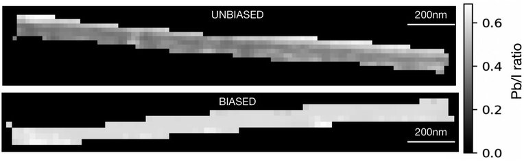 |
| | Fig. 6 Maps representing the calculated Pb/I ratio in the different samples. | |
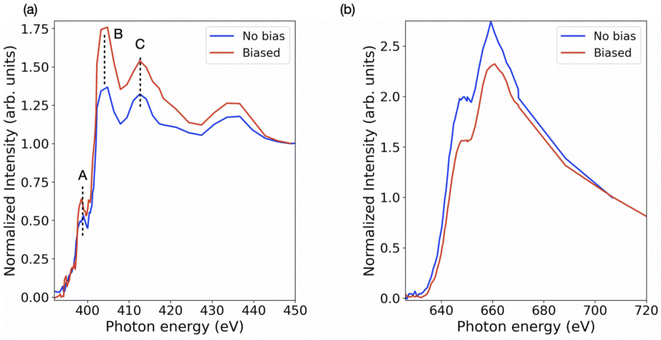 |
| | Fig. 7 Edge normalized average X-ray absorption spectra for biased and unbiased samples at (a) nitrogen K-edge and (b) iodine M-edge. | |
3 Conclusions
In the present work, we have reported the study of halide perovskite materials by a soft X-ray transmission spectromicroscopy technique. For both investigated MAPbI3 samples, we were able to gain key information regarding the variations in composition of specific components in the perovskite layer. Furthermore, we observed evidence of iodine ion diffusion in reverse biased samples. The oxygen content in the samples follows a distribution that is a consequence of the sample history and layer stacking in the production process. This initial work demonstrates the potential of using STXM to study the complex inhomogeneous and non-stoichiometric composition of the simple metal halide perovskite MAPbI3. Future work would include the application of the technique to i. a more statistically significant number of samples, ii. more complex perovskite formulations (triple cation, mixed 2D–3D, Pb-free), and iii. the study of variously stressed layers, varying both in nature (light soaking, electrical bias value and kinetic (dynamic or static), chemical treatment) and duration (few hours, days, or weeks) of the stress.
4 Experimental section
4.1 Sample fabrication
The ITO coated glass substrates (from Xin Yan Tech.) were cleaned in ultrasonic baths of acetone and isopropanol and then treated with UV-ozone for 15 minutes. A PEDOT:PSS hole transporting layer (approximately 50 nm thick) was then deposited on top of the ITO anode via spin-coating process (4500 rpm for 40 seconds) and baked at 120 °C for 20 minutes.
4.1.1 Reference samples of PbI2, PbO, MAI and MAPbI3. PbO (Sigma Aldrich, 99%), MAI (Greatcell Solar, >99.99%), PbI2 (Alpha Aesar, ultra-dry, 99.999%) and MAPbI3 films were prepared onto a Si3N4 window (50 nm thickness, frame size of 5 × 5 mm2, Norcada Inc., Edmonton, Canada). 0.05 M of PbO was dissolved in deionized water while MAI solution was prepared by dissolving MAI into N,N-dimethylformamide (DMF, Sigma Aldrich, anhydrous, 99.8%) with a concentration of 0.125 M. Both these films were spin-coated at 3000 rpm in a N2 environment. PbI2 of 50 nm thickness was prepared by sublimation in a vacuum chamber (pressure: 1.6 × 10⁻⁶ mbar) at 300 °C at a rate of 1 Å s−1. Reference MAPbI3 of 50 nm thickness was deposited by co-evaporation of PbI2 (deposition rate: 1 Å s−1) and MAI (deposition rate: 2.5 Å s−1) in a vacuum chamber (pressure: 1.6 × 10⁻⁶ mbar). The temperatures of PbI2 and MAI were maintained at 300 °C and 180 °C. A calibrated quartz crystal microbalance (QCM) sensor was used to monitor the deposition rate and deposited thickness of MAPbI3. For the perovskite samples: glass/ITO/PEDOT:PSS substrates were transferred into an N2-filled glovebox. A mix of PbI2 and CH3NH3I with a 1:1 molar ratio was solubilized in a mix of GBL-DMSO (8:2 volume ratio), and stirred for 1 h at 70 °C in N2 conditions before deposition. The filtered perovskite solution was spin-coated at 2500 rpm on the PEDOT:PSS layer. An anti-solvent treatment was performed by dropping 0.5 mL of toluene 5 seconds before the end of the spinning. The sample was then annealed for 1 minute at 70 °C and 5 minutes at 100 °C in N2 conditions. The thickness of the obtained active layer is between 250 and 300 nm. Following this to form an electron transporting layer, a 40 mg mL−1 solution of PC60BM in chlorobenzene was spin-coated at 2000 rpm for 30 seconds. The deposition was followed by a 3 minutes thermal annealing at 90 °C. The stack was then completed by depositing a 80 nm thick silver electrode via physical vapor deposition. For the 1 week biased sample, the device was biased using a homemade setup with a power supply set to −2 V, in N2 conditions, for 1 week. Samples were stored in an N2-filled sample box (to avoid air exposure) before being transferred for the FIB sectioning.
4.1.2 FIB preparation. Cross section lamellas of our bulk samples were prepared using the focus ion beam technique (FIB, Scios DualBeam). Before transferring the sample within the FIB dual beam microscope chamber, a thin layer of carbon (C) was deposited in order to avoid any electron and ionic beam charge effects that might appear during the preparation. At first, the area of interest is selected, and a 2/2/20 μm platinum (Pt) protective layer is deposited to protect the chosen area from excessive ion damage. Secondly, the selected area is isolated using the energetic gallium ion beam. Once the area is isolated, the milling process begins using a high current ion beam, and then as the lamella becomes thin (down to 0.8–1 μm), the ion beam current decreases. The lamella is then removed from the substrate with a micromanipulator and transferred to a TEM sample grid. A second milling process using very low ion beam currents, is performed to thin the lamella until its thickness is about 150–200 nm. The lamella obtained is then removed from the FIB and put under a controlled atmosphere into a transfer coffer in order to avoid air exposure during sample handling. We then transferred the sample to the STXM chamber for analysis. We note that damages to the very surface of the cross-section lamella in the FIB milling process cannot be ruled out completely. Following established protocols,52 we confirm that damages, if any, were minimized to the very surface of the lamella. The clear spectroscopic fingerprints of the organic molecules in the XAS spectra further confirm the absence of any significant damage and conversion of the film to PbI2.
4.2 STXM measurements
STXM measurements were performed on a Research Instruments (RI) STXM at the HERMES beamline53 at synchrotron SOLEIL. A Fresnel zone plate of 25 nm outermost ring width was used to focus a monochromatized X-ray beam on a raster scanned sample. A vacuum of 10−4 mbar was maintained during the entire measurement. Stacks were acquired across C, N, and O K-edges and I M-edge [270–750 eV] in three consecutive measurements with refocusing between each measurement. A dwell time of 5 ms and a step size of 10 nm was used to acquire stacks. Data analysis was performed using aXis2000 software.46
Author contributions
C. D., Y. B., P. S. and S. S. conceived the experiment. C. D., H. J. Y. B., D. T., B. G, J.-E. B. performed the experiments. C. D., H. J., S. S. and P. S. analysed and interpreted the data.
Conflicts of interest
There are no conflicts to declare.
Acknowledgements
The authors would like to thank Dr Minjin KIM for the biasing of samples, Dr Ileana FLOREA for the FIB preparation, Dr Maxime RIOULT for his help starting the collaboration between LPICM perovskite team and HERMES beamline. P. S. acknowledges the French Agence Nationale de la Recherche for funding under contract no. ANR-17-MPGA0012. Finally, authors acknowledge SOLEIL for the provision of synchrotron radiation facilities.
References
- A. Kojima, K. Teshima, Y. Shirai and T. Miyasaka, J. Am. Chem. Soc., 2009, 131, 6050–6051 CrossRef CAS PubMed.
- https://www.nrel.gov/pv/cell-efficiency.html.
- J. Tian, J. Wang, Q. Xue, T. Niu, L. Yan, Z. Zhu, N. Li, C. J. Brabec, H.-L. Yip and Y. Cao, Adv. Funct. Mater., 2020, 30, 2001764 CrossRef CAS.
- Y. Cui, C. Chen, C. Li, L. Chen, S. S. Bista, X. Liu, Y. Li, R. A. Awni, Z. Song and Y. Yan, ACS Appl. Mater. Interfaces, 2020, 12, 10588–10596 CrossRef CAS PubMed.
- P. Schulz, D. Cahen and A. Kahn, Chem. Rev., 2019, 119, 3349–3417 CrossRef CAS PubMed.
- S. Dunfield, A. Bojar, S. Cacovich, M. Frégnaux, T. Klein, R. Bramante, F. Zhang, D. Regaldo, V. Dufoulon, J.-B. Puel, G. Teeter, J. Luther, M. Bouttemy, D. Nordlund, K. Zhu, D. Moore, M. F. van Hest, J.-P. Kleider, J. Berry and P. Schulz, Cell Rep. Phys. Sci., 2021, 2, 100520 CrossRef CAS.
- A. Kumar, A. Rana, N. Vashistha, K. K. Garg and R. K. Singh, Sol. Energy, 2020, 211, 345–353 CrossRef CAS.
- H.-S. Kim, I.-H. Jang, N. Ahn, M. Choi, A. Guerrero, J. Bisquert and N.-G. Park, J. Phys. Chem. Lett., 2015, 6, 4633–4639 CrossRef CAS.
- P. Calado, A. M. Telford, D. Bryant, X. Li, J. Nelson, B. C. O'Regan and P. R. Barnes, Nat. Commun., 2016, 7, 1–10 Search PubMed.
- C. L. Watts, L. Aspitarte, Y.-H. Lin, W. Li, R. Elzein, R. Addou, M. J. Hong, G. S. Herman, H. J. Snaith and J. G. Labram, Commun. Phys., 2020, 3, 1–10 CrossRef.
- E. Mosconi, D. Meggiolaro, H. J. Snaith, S. D. Stranks and F. De Angelis, Energy Environ. Sci., 2016, 9, 3180–3187 RSC.
- A. J. Knight, A. D. Wright, J. B. Patel, D. P. McMeekin, H. J. Snaith, M. B. Johnston and L. M. Herz, ACS Energy Lett., 2018, 4, 75–84 CrossRef.
- M. C. Brennan, A. Ruth, P. V. Kamat and M. Kuno, Trends Chem., 2020, 2, 282–301 CrossRef CAS.
- E. T. Hoke, D. J. Slotcavage, E. R. Dohner, A. R. Bowring, H. I. Karunadasa and M. D. McGehee, Chem. Sci., 2015, 6, 613–617 RSC.
- Z.-J. Yong, S.-Q. Guo, J.-P. Ma, J.-Y. Zhang, Z.-Y. Li, Y.-M. Chen, B.-B. Zhang, Y. Zhou, J. Shu and J.-L. Gu, et al., J. Am. Chem. Soc., 2018, 140, 9942–9951 CrossRef CAS.
- J.-P. Ma, J. Yin, Y.-M. Chen, Q. Zhao, Y. Zhou, H. Li, Y. Kuroiwa, C. Moriyoshi, Z.-Y. Li and O. M. Bakr, et al., ACS Mater. Lett., 2019, 1, 185–191 CrossRef CAS.
- F. Ye, W. Tang, F. Xie, M. Yin, J. He, Y. Wang, H. Chen, Y. Qiang, X. Yang and L. Han, Adv. Mater., 2017, 29, 1701440 CrossRef PubMed.
- S. Cacovich, L. Cinà, F. Matteocci, G. Divitini, P. A. Midgley, A. Di Carlo and C. Ducati, Nanoscale, 2017, 9, 4700–4706 RSC.
- F. Matteocci, Y. Busby, J.-J. Pireaux, G. Divitini, S. Cacovich, C. Ducati and A. Di Carlo, ACS Appl. Mater. Interfaces, 2015, 7, 26176–26183 CrossRef CAS PubMed.
- H. Lee, S. Gaiaschi, P. Chapon, A. Marronnier, H. Lee, J.-C. Vanel, D. Tondelier, J.-E. Bourée, Y. Bonnassieux and B. Geffroy, ACS Energy Lett., 2017, 2, 943–949 CrossRef CAS.
- S. Béchu, M. Ralaiarisoa, A. Etcheberry and P. Schulz, Adv. Energy Mater., 2020, 10, 1904007 CrossRef.
- Z. Xiao, Y. Yuan, Y. Shao, Q. Wang, Q. Dong, C. Bi, P. Sharma, A. Gruverman and J. Huang, Nat. Mater., 2015, 14, 193–198 CrossRef CAS PubMed.
- A. Pockett, G. E. Eperon, T. Peltola, H. J. Snaith, A. Walker, L. M. Peter and P. J. Cameron, J. Phys. Chem. C, 2015, 119, 3456–3465 CrossRef CAS.
- V. M. Le Corre, E. A. Duijnstee, O. El Tambouli, J. M. Ball, H. J. Snaith, J. Lim and L. J. A. Koster, ACS Energy Lett., 2021, 6, 1087–1094 CrossRef CAS.
- A. P. Hitchcock, J. Electron Spectrosc. Relat. Phenom., 2015, 200, 49–63 CrossRef CAS.
- T. H. Yoon, S. B. Johnson, K. Benzerara, C. S. Doyle, T. Tyliszczak, D. K. Shuh and G. E. Brown, Langmuir, 2004, 20, 10361–10366 CrossRef CAS PubMed.
- H. Bluhm, K. Andersson, T. Araki, K. Benzerara, G. E. Brown, J. J. Dynes, S. Ghosal, M. K. Gilles, H.-C. Hansen and J. Hemminger, et al., J. Electron Spectrosc. Relat. Phenom., 2006, 150, 86–104 CrossRef CAS.
- B. Rösner, S. Finizio, F. Koch, F. Döring, V. A. Guzenko, M. Langer, E. Kirk, B. Watts, M. Meyer and J. L. Ornelas, et al., Optica, 2020, 7, 1602–1608 CrossRef.
- H. Ade, X. Zhang, S. Cameron, C. Costello, J. Kirz and S. Williams, Science, 1992, 258, 972–975 CrossRef CAS.
- C. R. McNeill, B. Watts, L. Thomsen, W. J. Belcher, N. C. Greenham and P. C. Dastoor, Nano Lett., 2006, 6, 1202–1206 CrossRef CAS.
- C. R. McNeill, B. Watts, L. Thomsen, H. Ade, N. C. Greenham and P. C. Dastoor, Macromolecules, 2007, 40, 3263–3270 CrossRef CAS.
- C. McNeill, B. Watts, S. Swaraj, H. Ade, L. Thomsen, W. Belcher and P. Dastoor, Nanotechnology, 2008, 19, 424015 CrossRef CAS PubMed.
- S. Swaraj, C. Wang, H. Yan, B. Watts, J. Luning, C. R. McNeill and H. Ade, Nano Lett., 2010, 10, 2863–2869 CrossRef CAS PubMed.
- J. R. Moore, S. Albert-Seifried, A. Rao, S. Massip, B. Watts, D. J. Morgan, R. H. Friend, C. R. McNeill and H. Sirringhaus, Adv. Energy Mater., 2011, 1, 230–240 CrossRef CAS.
- W. Zhang, M. Lin, A. Winesett, O. Dhez, A. L. Kilcoyne, H. Ade, M. Rubinstein, K. Shafi, A. Ulman and D. Gersappe, et al., Polym. Adv. Technol., 2011, 22, 65–71 CrossRef CAS.
- B. Watts, S. Swaraj, D. Nordlund, J. Lüning and H. Ade, J. Chem. Phys., 2011, 134, 024702 CrossRef CAS PubMed.
- S. Pack, E. Bobo, N. Muir, K. Yang, S. Swaraj, H. Ade, C. Cao, C. S. Korach, T. Kashiwagi and M. H. Rafailovich, Polymer, 2012, 53, 4787–4799 CrossRef CAS.
- B. A. Collins and H. Ade, J. Electron Spectrosc. Relat. Phenom., 2012, 185, 119–128 CrossRef CAS.
- J. Dhar, T. Mukhopadhay, N. Yaacobi-Gross, T. D. Anthopoulos, U. Salzner, S. Swaraj and S. Patil, J. Phys. Chem. B, 2015, 119, 11307–11316 CrossRef CAS PubMed.
- Q. Arnoux, B. Watts, S. Swaraj, F. Rochet and L. Tortech, Nano Res., 2018, 11, 2771–2782 CrossRef CAS.
- H. Jun, H. R. Lee, D. Tondelier, B. Geffroy, P. Schulz, J.-É. Bourée, Y. Bonnassieux and S. Swaraj, Sci. Rep., 2022, 12, 1–11 CrossRef PubMed.
- M.-W. Lin, K.-C. Wang, J.-H. Wang, M.-H. Li, Y.-L. Lai, T. Ohigashi, N. Kosugi, P. Chen, D.-H. Wei and T.-F. Guo, et al., Adv. Mater. Interfaces, 2016, 3, 1600135 CrossRef.
- M.-H. Li, H.-H. Yeh, Y.-H. Chiang, U.-S. Jeng, C.-J. Su, H.-W. Shiu, Y.-J. Hsu, N. Kosugi, T. Ohigashi and Y.-A. Chen, et al., Adv. Mater., 2018, 30, 1801401 CrossRef.
- P. Schulz, ACS Energy Lett., 2018, 3, 1287–1293 CrossRef CAS.
- I. Koprinarov, A. Hitchcock, C. McCrory and R. Childs, J. Phys. Chem. B, 2002, 106, 5358–5364 CrossRef CAS.
- http://unicorn.chemistry.mcmaster.ca/aXis2000.html.
- P. V. Kamat and M. Kuno, Acc. Chem. Res., 2021, 54, 520–531 CrossRef CAS PubMed.
- M. Abdi-Jalebi, Z. Andaji-Garmaroudi, S. Cacovich, C. Stavrakas, B. Philippe, J. M. Richter, M. Alsari, E. P. Booker, E. M. Hutter and A. J. Pearson, et al., Nature, 2018, 555, 497–501 CrossRef CAS PubMed.
- R. A. Belisle, K. A. Bush, L. Bertoluzzi, A. Gold-Parker, M. F. Toney and M. D. McGehee, ACS Energy Lett., 2018, 3, 2694–2700 CrossRef CAS.
- G. J. Man, C. M. Sterling, C. Kamal, K. A. Simonov, S. Svanström, J. Acharya, F. O. Johansson, E. Giangrisostomi, R. Ovsyannikov and T. Huthwelker, et al., Phys. Rev. B, 2021, 104, L041302 CrossRef CAS.
- C. Kolczewski, R. Püttner, O. Plashkevych, H. Ågren, V. Staemmler, M. Martins, G. Snell, A. Schlachter, M. Sant'Anna and G. Kaindl, et al., J. Chem. Phys., 2001, 115, 6426–6437 CrossRef CAS.
- F. U. Kosasih, G. Divitini, J. F. Orri, E. M. Tennyson, G. Kusch, R. A. Oliver, S. D. Stranks and C. Ducati, Microsc. Res. Tech., 2022, 2351–2355 CrossRef CAS PubMed.
- R. Belkhou, S. Stanescu, S. Swaraj, A. Besson, M. Ledoux, M. Hajlaoui and D. Dalle, J. Synchrotron Radiat., 2015, 22, 968–979 CrossRef PubMed.
|
| This journal is © The Royal Society of Chemistry 2022 |
Click here to see how this site uses Cookies. View our privacy policy here. 
 Open Access Article
 This Open Access Article is licensed under a Creative Commons Attribution-Non Commercial 3.0 Unported Licence
 be,
Jean-Eric Bouréeb,
Yvan Bonnassieuxb,
Philip Schulz
be,
Jean-Eric Bouréeb,
Yvan Bonnassieuxb,
Philip Schulz