
 Open Access Article
 This Open Access Article is licensed under a Creative Commons Attribution-Non Commercial 3.0 Unported Licence
PBEsol/HSE functional: a promising candidate for vanadium dioxide (B) characterization
Elaheh Mohebbia,
Eleonora Pavoni a,
Davide Mencarellib,
Pierluigi Stipaa,
Luca Pierantonib and
Emiliano Laudadio*a
a,
Davide Mencarellib,
Pierluigi Stipaa,
Luca Pierantonib and
Emiliano Laudadio*a
aDepartment of Materials, Environmental Sciences and Urban Planning, Marche Polytechnic University, Ancona 60131, Italy. E-mail: e.mohebbi@staff.univpm.it; e.pavoni@staff.univpm.it; p.stipa@staff.univpm.it; e.laudadio@staff.univpm.it
bInformation Engineering Department, Marche Polytechnic University, Ancona 60131, Italy. E-mail: l.pierantoni@staff.univpm.it; d.mencarelli@staff.univpm.it
First published on 1st November 2022
Abstract
A VO2(B) polymorph has been thoroughly investigated by means of density functional theory (DFT) calculations to evaluate the structure, Raman spectrum, cohesive energy, phonon band structure, an delectronic and optical properties. Among the computed Raman modes, eight of them have been assigned to the VO2(B) structure in full agreement with the corresponding experimental spectra. The minimized structure of the VO2(B) polymorph indicated the presence of negative frequencies in its phonon dispersion curves, confirming the dynamic instability of this material. Herein, the combination of generalized gradient approximation (GGA)/PBEsol with a hybrid HSE functional has been employed to perform ab initio calculations on VO2(B), since the conventional semi-local DFT calculations are believed to underestimate the band gap of materials. By considering the electronic structure calculations, for the first time, we found that the calibration of the PBEsol functional can efficiently model the metallic-like properties of VO2(B) with a band gap of 0.26 eV, while the corresponding electronic bandgap of VO2(B) based on the HSE functional possesses a larger band gap of 0.67 eV. The prediction of optical characteristics of VO2(B) indicated that the optical conductivity of VO2(B) lies in the infrared region of light. This work strongly suggests the combination of GGA/PBEsol with HSE hybrid functionals to carefully describe the physical properties of smart materials exploitable in electronics and optoelectronics applications. The nanostructure of VO2(B) looks promising for IR photodetectors and smart windows applications as a semiconductor material with excellent optical features. It is predicted that in the future VO2(B) will continue to expand the envelope of its capabilities because of its remarkable properties.
Introduction
Vanadium dioxide (VO2) material shows a reversible metal-to-insulator (MIT) transition at the critical temperature of 340 K, where a structural phase transition takes place from high temperature metallic tetragonal rutile VO2(R) to insulator low temperature monoclinic VO2(M).1,2 Across the MIT transition, VO2 polymorphs offer significant changes in physical properties such as stability, magnetic and electronic properties, electrical resistance, and optical conductivity in response to different external stimuli including temperature, light, and electric field.3–6 This characteristic made VO2 a material with widespread interest for electronics and optoelectronics applications like memory devices,7 Mott field effect transistor (FET),8 smart windows,9 and VO2-based photodetectors.10Among the different low temperature polymorphs of the VO2 family, consisting of VO2(M),11 VO2(A),12 and VO2(B),13 this last is characterized by the space group C2/m and it strongly desired to effectively act as a cathode material in Li ion batteries and supercapacitors.14,15 In addition, this allotropic phase has shown to be a unique thermal sensing material in uncooled IR detectors.16 Moreover, this polymorph has a rich electronic phase diagram that exhibits a broad metallic to insulator transition by cooling from 300 K to 100 K.17 According to the experimental and theoretical published data, the band gap ∼0.6–0.7 eV13,17–19 was reported for insulating VO2(B); however, X-ray photoelectron spectroscopy studies suggested even larger band gap for this polymorph.20
The characterization of the physicochemical properties of VO2(B) nanostructure represents an attractive research topic. Wan et al.18 experimentally investigated the Raman spectra for the VO2(B) thin films and reported three Raman modes centered at 103, 193, and 296 cm−1 for VO2(B) thin film, in a good agreement with previous outcomes by Wang et al.21 obtained by RF magnetron sputtering analysis. Also, they considered the electronic and optical properties of this nanostructure with an electronic band gap of 0.6 eV as well as optical absorption in the infrared range predicted by DFT + U calculations. Zhang et al.19 investigated the phase transition from VO2(B) to VO2(A) phases by X-ray absorption spectroscopy measurements and first-principles calculations. According to the corresponding findings, they have outlined the metastability of VO2(B) in comparison with two other phases of VO2(R) and VO2(M). They found the less geometrical stability of the VO2(B) phase by a formation energy of −6.66 eV, in comparison to −6.93 and −7.18 eV for VO2(R) and VO2(M), respectively. In this study, also the electronic property has been evaluated by Heyd–Scuseria–Ernzerhof (HSE) hybrid functional calculations, and a 0.65 eV band gap has been found, leading to a semiconducting feature for this structure. Further, Lee et al.22 used the DFT calculations to characterize the electronic features of the A, B, and M phases of VO2. The results revealed that upon applying the standard DFT calculations, the zero-band gap was observed for all phases, whereas hybrid functional PBE0 calculations yielded the bandgap 0.6 and 0.5 eV for M and A phases respectively, and a very narrow value of 25 meV for the VO2(B) polymorph. Moreover, to assess the optical properties, they measured the optical conductivity of all three geometries, reporting the optical band gap of 0.6 eV, 0.5 eV, and 0.0 eV for M, A, and B phases, respectively.
From these considerations, there have been some studies about the MIT, electronic, and optical properties of VO2(B), although the corresponding outcomes are controversial. Moreover, there are no experimental/theoretical results available on its phonon dispersion calculations, and Raman spectra never predicted by ab initio calculations for VO2(B) nanostructure yet. Hence, in this study, we employ DFT calculations to estimate the properties of VO2(B) polymorph. We designed a simple and convenient route to utilize advanced theoretical methods to evaluate the optimized structure and material characteristics of the VO2(B) polymorph. The main objectives of this work are (i) investigation of the structural parameters of VO2(B) by employing PBEsol exchange-correlation (XC) functional to find the most accurate optimized geometry, (ii) evaluation of the corresponding Raman spectra to verify the experimental observed modes, (iii) calculation of phonon band structure to examine the dynamical stability of this polymorph, (iv) analysis of the electronic and optical properties with GGA/PBEsol and the most accurate HSE hybrid functionals.
Computational methods
The density-functional-theory (DFT) calculations were carried out using Quantum ESPRESSO (QE)23 and QuantumATK (QATK)24 codes. The Kohn–Sham (KS) formulation25,26 has been resolved within the framework of the plane-wave (PW) basis set. The scalar-relativistic projector-augmented wave method27 was adopted, with a pseudopotential (PP) treating the V-3d and O-2p as valence orbitals. We performed complete optimization of the cell volume, shape, and atomic positions, with the PBEsol28 semi-local XC functional. Valence orbitals were set with a kinetic energy cut-off of 70 Ry. Brillouin-zone (BZ)29 has a limited gamma point, and a smearing parameter of 0.01 Ry has been considered for the electron population function.30 Broyden–Fletcher–Goldfarb–Shanno (BFGS) algorithm was employed for unit cell optimization.31The unit cell shape and atomic positions were allowed to relax until the force on each atom with 1 × 10⁻⁶ eV Å−1 and total energy was 1 × 10⁻⁵ eV Å−1. Raman spectrum was simulated based on numerical linear combination of atomic orbitals (LCAO) basis set employing local-density approximations (LDA) XC and Perdew–Zunger (PZ) PP implemented in QATK package, with a dynamical matrix 3 × 3 × 3 to calculate the phonon modes. To consider the dynamic stability of VO2(B), the phonon frequencies were calculated using the density functional perturbation theory (DFPT).32 Moreover, the electronic properties have been investigated by the band structure and projected density of states (PDOS) calculations based on PBEsol and PBEsol/HSE33 using self-consistent field (SCF) and non-self-consistent (NSCF) calculations performed with 6 × 6 × 6 and 12 × 12 × 12 Monkhorst–Pack mesh, respectively. Finally, optical calculations were analyzed based on random phase approximation (RPA)34,35 over the PBEsol and PBEsol/HSE results. Optical properties for VO2(B) polymorph were computed by QATK package. In the corresponding input files, we chosen the functional (PBEsol or PBEsol + HSE), k-points and cut-off energy in the same value of optimized unit cell, broadening of 0.1 eV, and number of the bands supposed to be 200 bands below and above the Fermi level. XCRYSDEN graphical package has been used to generate structures and visualizations.36
Results and discussion
Analysis of structural parameters and Raman spectra
VO2(B) polymorph has a low-symmetry base-centered monoclinic structure with a space group of C2/m and lattice constant a = 11.85 Å, b = 3.74 Å, and c = 6.19 Å, as schematically shown in Fig. 1. This nanostructure can be considered of two identical atom layers including 3D frameworks of VO6 octahedra, where VO6 are linked by oxygen atoms in the corners. The structure contains two vanadium sites labeled V1 and V2; both cations are off-centered, resulting in the presence of alternate short/long V–V bond distances. The VO2(B) unit cell includes 24 atoms in the conventional unit cell with 8 vanadium and 16 oxygen (see Fig. 1) atoms. In this study, VO2(B) polymorph has been simulated initially by the available information about the lattice dimensions, V–V and V–O bond length have been reported in experimental6 and theoretical18,19 studies. PBE XC functional has been used to obtain optimized geometry of VO2(B) nanostructure.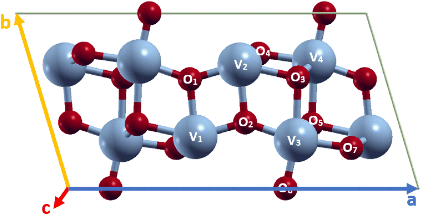 | ||
| Fig. 1 Schematic representations of VO2(B) unit cell, color code in the ball and stick model: V blue and O red. | ||
After lattice optimization, we evaluated the structural parameters and bond lengths on different types of V–V and V–O atomic distances in the 3D structure. The calculated structural parameters for monoclinic VO2(B) are shown in Table 1, together with similar results for comparison obtained from the previous experimental6 and theoretical outcomes.18,19 Inspection of the outcomes in Table 1 reveals that the central VO6 octahedra with V2 called atom, sharing an edge with V1 cation along the ab plane with bond distance 2.87 Å, while in the same plane share its oxygen atom with V3 with bond length 3.18 Å along the zigzag direction. The share reached either in the ab plane by V4 with long bond distance 3.31 Å and in the ac plane with V3–V4 by medium bond distance 3.09 Å, respectively. It is to underline that the V3–O3 bond distance (2.11 Å) is slightly longer than that of V2–O1 (1.76 Å) and V2–O2 (1.96 Å), while V3–O6 showed the shortest value with 1.67 Å. However, V3–O2 and V3–O7 indicate similar bond distances (1.82 Å and 1.89 Å) shorter than V3–O5 with 2.02 Å.
| Our study | Ref. 19 | Ref. 18 | Ref. 6 | ||||
|---|---|---|---|---|---|---|---|
| V1–V2 | 2.87 | V–O | 1.65 | V–O | 1.92 | V–V | 2.89 |
| V2–V3 | 3.18 | V–O | 2.17 | V–O | 1.91 | V–V | 3.24 |
| V2–V4 | 3.31 | V–O | 1.99 | V–O | 2.14 | V–V | 3.33 |
| V3–V4 | 3.09 | V–O | 1.95 | V–O | 1.91 | V–V | 3.06 |
| V2–O1 | 1.76 | V–O | 1.98 | V–O | 1.90 | ||
| V2–O2 | 1.96 | V–O | 1.91 | V–O | 2.03 | ||
| V2–O3 | 2.02 | V–O | 2.15 | V–O | 1.89 | ||
| V2–O4 | 2.01 | V–O | 1.90 | V–O | 1.66 | ||
| V3–O2 | 1.82 | V–O | 1.82 | V–O | 1.93 | ||
| V3–O3 | 2.11 | V–O | 2.03 | ||||
| V3–O5 | 2.02 | ||||||
| V3–O6 | 1.67 | ||||||
| V3–O7 | 1.89 | ||||||
The determined structural parameters of V–V and V–O bond distances existing in Table 1 show that the V–V bonds are in excellent agreement with those reported in ref. 6. When we compared our results with the theoretical results in ref. 18,19, we found the shortest V–O bond length of 1.67 Å in comparison to 1.66 Å and 1.65 Å obtained from ref. 18 and 19, respectively. On the other hand, we detected the longest V–O bond distance of 2.11 Å with respect to 2.14 Å and 2.17 Å predicted in ref. 18 and 19, respectively. About the other V–O bond lengths, the average bond length was 1.91 Å compared with 1.94 Å in ref 18 and 1.95 Å in ref. 19, respectively. So, from all these compared data we can confirm that structural parameters from optimized geometry in this study is in very good agreement with the experimental and theoretical studies.6,18,19
The Raman spectrum of the VO2(B) polymorph is shown in Fig. 2, which shows a series of bands at 0–940 cm−1 related to the vibrational modes of V–O. From the results obtained in our study, the main peaks of this polymorph were calculated to be at 144, 185, 246, 310, 370, 507, 624, and 790 cm−1. Fig. 2 reveals that the intense peak at 144 cm−1 could be attributed to lattice vibrations of VO2(B) structure and the peak centered at 790 cm−1 could be assigned to V–O high stretching frequency. Other medium-frequency peaks visible at about 246 and 310 could be attributed to V–O–V bending and those located at 370 and 507 can be related to V–O–V bridging modes of this structure, respectively.
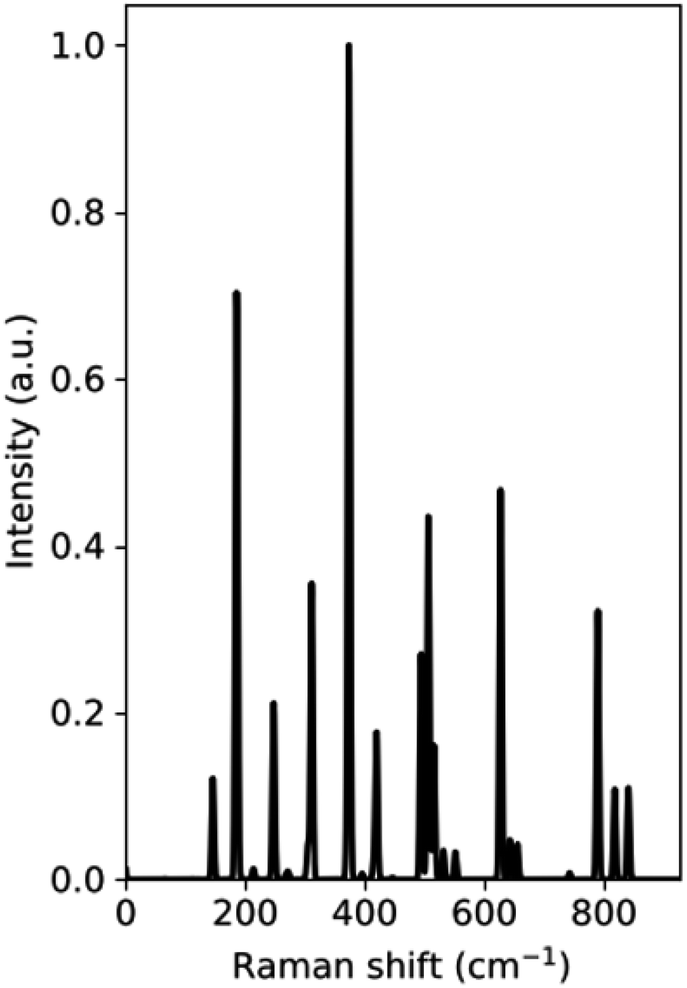 | ||
| Fig. 2 DFT-based Raman spectra of VO2(B) polymorph. | ||
According to experimental results by Wang et al.,21 Raman bands of VO2(B) film exist in three regions consisting of yellow, white, and dark by using laser light analysis. While for the white region the peaks are not intense, the yellow region indicates intense bands centered at 102, 193, 295, 393, 462, 662, and 900 cm−1, and the dark region shows intense peaks positioned at 132, 203, 303, 416, 504, 529 and 700 cm−1. In another experimental study by Sone et al.,37 VO2(B) thin film with a base-centered monoclinic crystal structure have Raman bands in 144, 287, 487, 679, and 917 cm−1. The observed room temperature nine peaks located at 142, 192, 222, 259, 308, 338, 388, 498, and 613 cm−1 corresponding to the phonon modes of the monoclinic phase for VO2 also confirmed our calculations for this polymorph.38 By comparing the Raman spectrum of VO2(B) polymorph from our calculations with those of VO2(B) nanobelts39 and VO2(B) thin films,21,37,38,40 we found that the peak positions of vibrational modes are slightly different in intensity because of different condition between theory and experiment.
Geometrical and dynamic stability
In order to evaluate the geometrical stability of VO2(B) polymorph, we calculated the cohesive energy per atom using the following eqn (1):| Ecohesive/atom = (Etotal − nVEV − n0E0)/M | (1) |
The study of phonon dispersions of VO2(B) is expected to give useful information about the dynamical stability of this polymorph. The phononic dispersion bands were calculated for the VO2(B) structure along with the directions of high-symmetry points of G–X–M–Y–I–G in the first BZ (see Fig. 3). The inspection of dispersion curves in Fig. 3 reveals that the dynamic matrix has imaginary eigenvalues for acoustic modes (negative frequencies around −30 cm−1), which provides a sign of phonon softening instabilities of this material. While there are no first-principal DFT calculations of phonon frequencies of VO2(B) for comparison, the result is indeed consistent with the experiments,6,13,44 in which the metastability of this polymorph has been observed. Similarly, Kim et al.45 performed DFT calculations to investigate the phonon dispersion curves for rutile (R) and monoclinic (M) polymorphs of VO2 and they have demonstrated phonon softening instabilities for both structures with the presence of negative phonon frequencies around −30 meV at gamma point in reciprocal space.
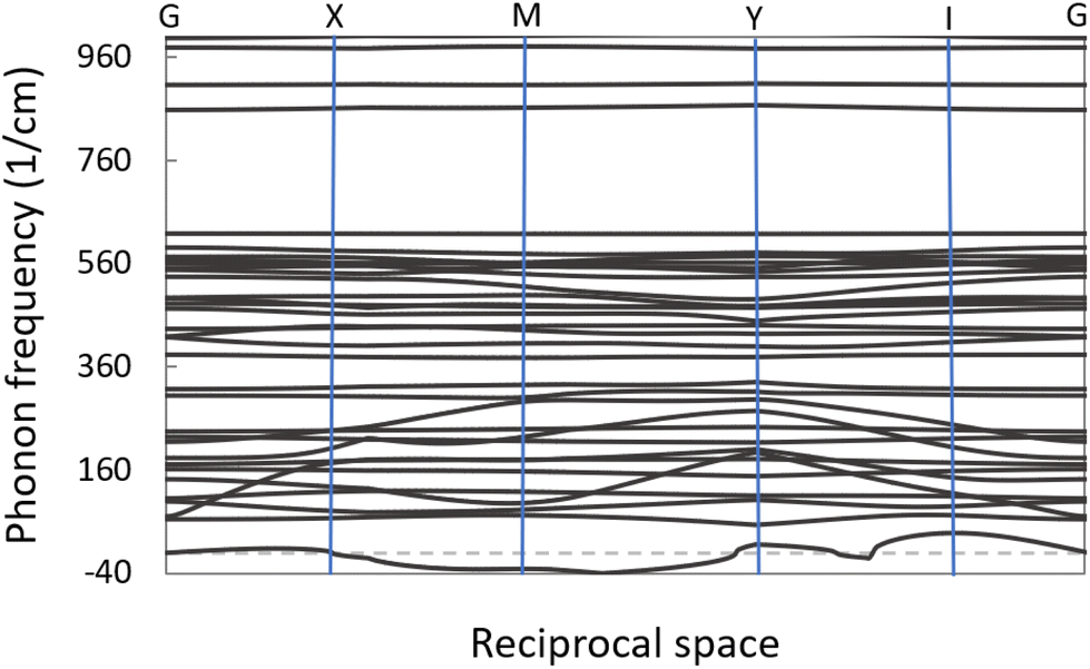 | ||
| Fig. 3 Phonon frequencies of VO2(B) polymorph with the high symmetry points of the first BZ. | ||
Electronic and optical properties
With the aim to study the electronic properties of the VO2(B) structure, band structure and PDOS curves for V-3d, O-2p, and total DOS were computed based on the PBEsol and PBEsol + HSE approximations. An inspection of Fig. 4 indicates that with both functionals the main contribution of total DOS belonged to the V-3d orbitals accompanied by less contribution from the O-2p states. The results obtained by band structure calculations revealed that a very narrow band gap of 0.26 eV for VO2(B) polymorph estimated with PBEsol XC functional, with valence and conduction band edges −0.09 eV and 0.17 eV, respectively.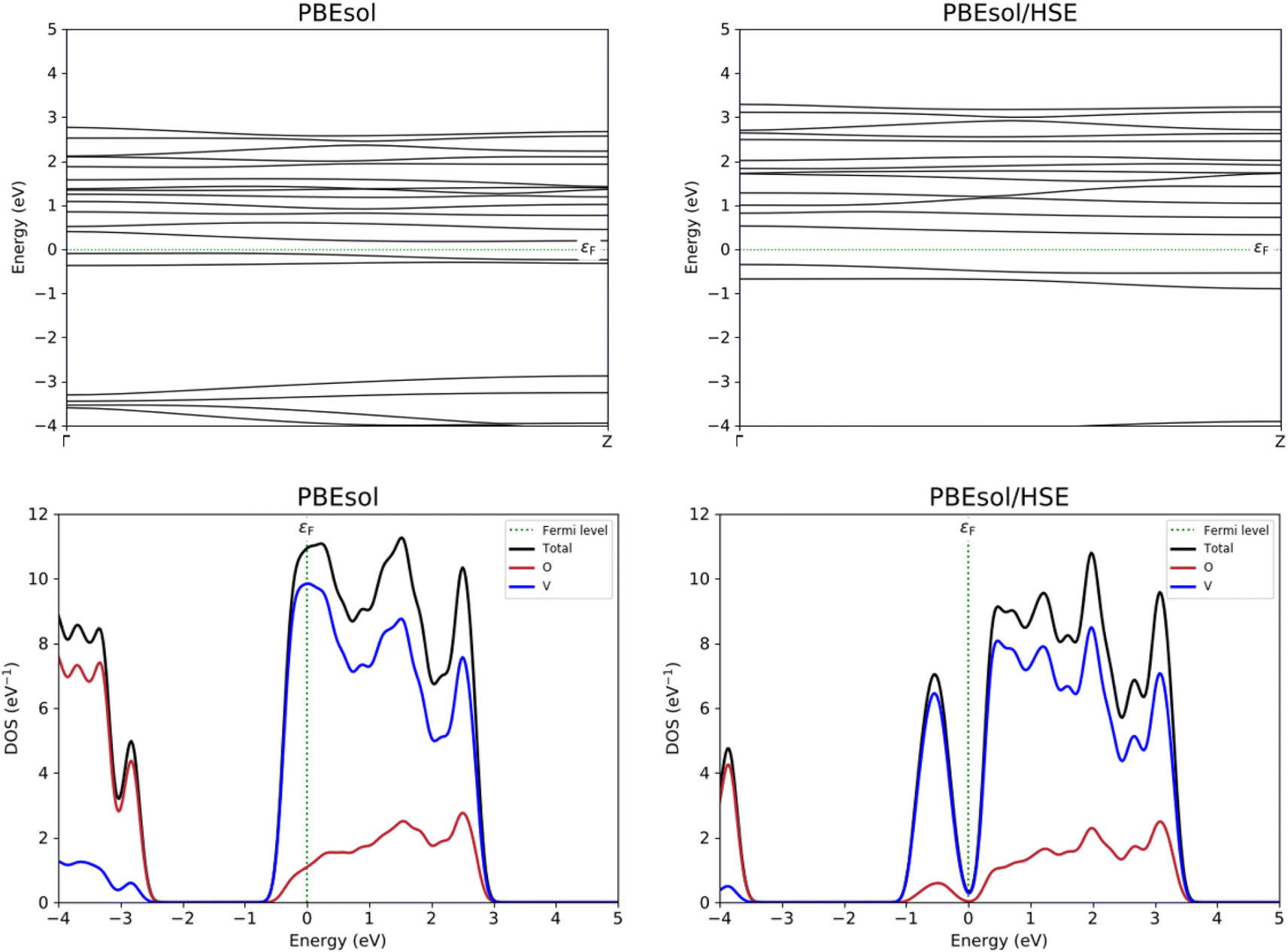 | ||
| Fig. 4 Band structure and PDOS calculations of VO2(B) polymorph predicted by PBEsol and PBEsol/HSE functionals. Fermi energy is aligned to zero. | ||
Since GGA potential approximations severely underestimate the band gap values in solids,46 the PDOS of the VO2(B) phase is also calculated with the HSE hybrid functional, a more resource demanding calculation as a consequence of the more accurate functional than conventional GGA. The corresponding bandgap of VO2(B) based on HSE functional possesses a larger band gap of 0.67 eV with respect to that predicted by GGA/PBEsol, with the highest occupied and lowest unoccupied orbital levels of 0.32 eV and −0.35 eV, respectively. The computed band gap value by HSE approximation for the optimized structure of VO2(B) is comparable with theoretical calculations result of about 0.65 eV using PBE/HSE hybrid functional in ref. 19 and 0.60 eV predicted by DFT + U in ref. 18, and very interestingly well describe the experimental value 0.7 eV.13,17,18
In an experimental work by Lourembam et al.,17 they investigated the photoinduced insulator-to-metal transition in VO2(B) using the temperature-dependent optical pump-probe technique. This study reported the metallic phase (300 K) and the insulating phase (100 K) of this structure, respectively; however, the insulating phase can be indicated by two electronic relaxation times and the metallic phase showed only one characteristic time. In this work, for the first time, they demonstrated that the low temperature insulating state can fall into a ‘metallic-like’ state and by increasing the temperature the metallic phase can be reached. While they did not report the experimental electronic band gaps values for these three states, our outcomes computed by PBEsol and PBEsol/HSE can significantly display the experimental metallic-like and insulating phases of VO2(B) by electronic band gap 0.26 eV and 0.67 eV, respectively. Therefore, the good agreement between DFT calculations and experimental observations strongly suggests that these functionals are effectively describe the electronic properties observed in VO2(B) structure.
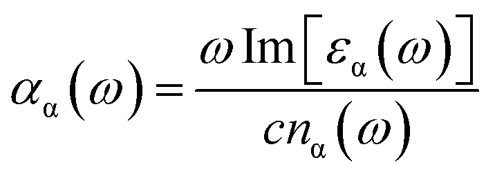
Next, we focus on the optical properties of VO2(B) with optical absorption spectra, optical conductivity, reflective index and extinction coefficient calculated within RPA + PBEsol and RPA + PBEsol/HSE functionals. We considered the parallel (a-in-plane) and perpendicular (z-out-of-plane) polarization directions of this polymorph. We discuss the absorption coefficient (αα(ω)), which ascribed by eqn (2):47
 | (2) |
It is worthy to notice that dielectric function can be describe by two components:
| ε(ω) = ε1(ω) + iε2(ω) | (3) |
The imaginary part can be demonstrated with the following eqn (4):
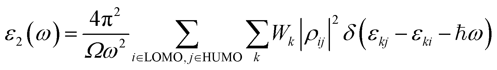 | (4) |
While the real part can discuss using the eqn (5):
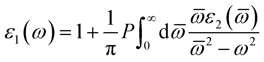 | (5) |
These two components of dielectric function can provide important information to the nature of dielectric materials. While the real dielectric constant indicates the amount of the material polarization, the imaginary dielectric constant reveals the measure of the dielectric losses.
The absorption coefficient for VO2(B) polymorph, calculated by PBEsol (a and c) and PBEsol/HSE (b and d) functionals, has been plotted in Fig. 5. Here, we also reported the acquired results in the visible range (from 380 to 780 nm) as a function of wavelength, for our system. Based on this figure and the range of photon energy, the maximum absorption coefficients with the PBEsol are 6.0 × 105 cm−1 and 3.1 × 105 cm−1, and the corresponding values predicted by PBEsol/HSE are 3.2 × 105 cm−1 and 4.6 × 105 cm−1, along the in-plane and out-of-plane polarizations direction, respectively. The outcomes indicate that the first main peaks of absorption coefficient of VO2(B) are located at 0.35 eV and 0.65 eV for PBEsol and 0.75 eV and 0.98 eV calculated with HSE, along the in-plane and out-of-plane polarization directions, respectively. Moreover, our results reveal that VO2(B) has its intense adsorption in the ultraviolet range (300 nm) by PBEsol and Infrared range (830 nm) according to PBEsol/HSE approximations (Fig. 5c and d).
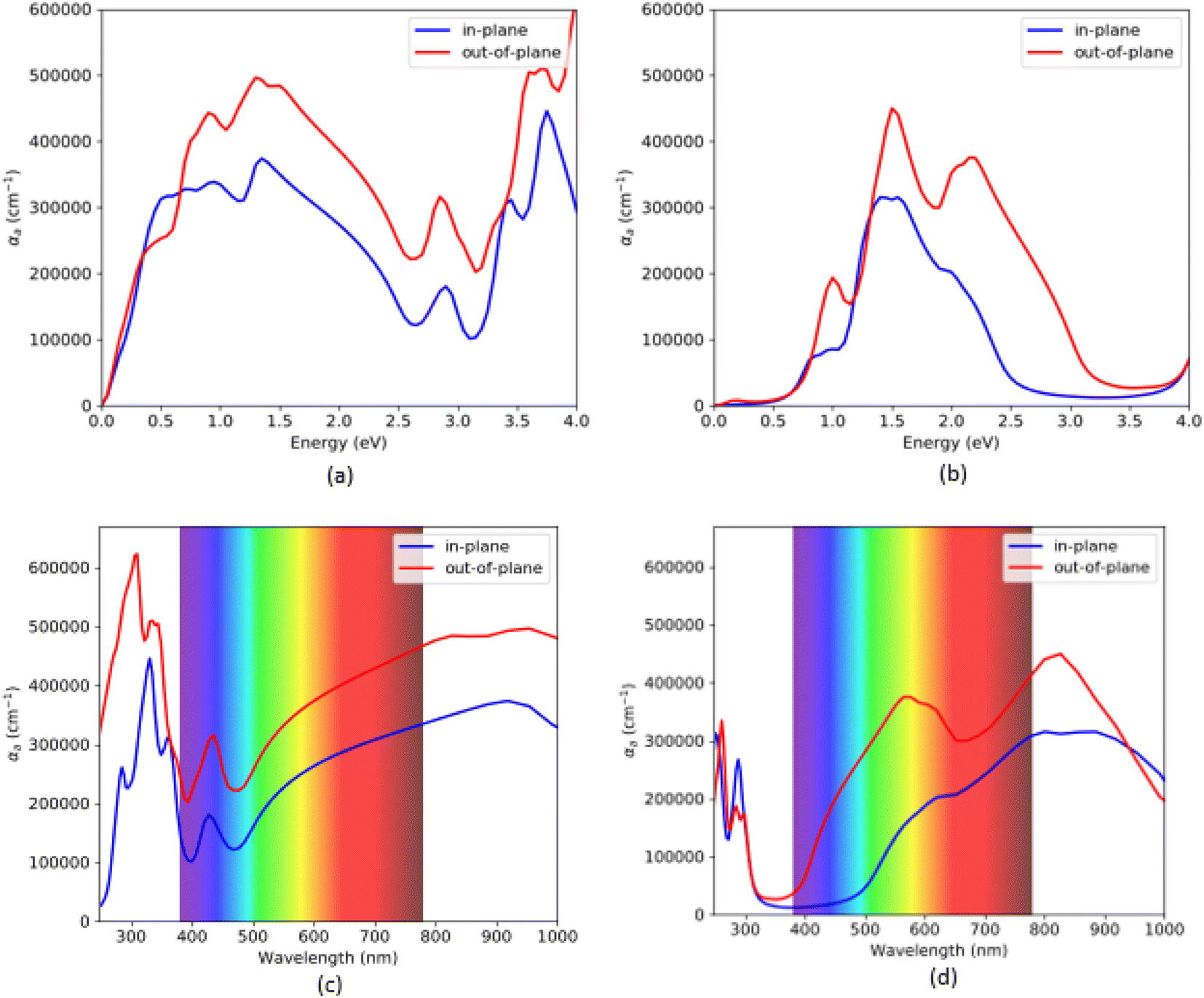 | ||
| Fig. 5 Optical absorption spectra as functions of energy and wavelength, of VO2(B) polymorph along with in-plane and out-of-plane directions predicted by PBEsol (a and c) and PBEsol/HSE (b and d), respectively. | ||
We next discuss the optical conductivity Re[σ(ω)] of VO2(B) structure. The real part of the optical conductivity can be described as follows:
 | (6) |
The optical conductivity spectra of VO2(B) polymorph, computed by both PBEsol and PBEsol/HSE, are presented in Fig. 6(a–d) as functions of energy (eV) and wavelength (nm). The optical conductivities began with a high tensity in PBEsol calculations, while the intensity of peaks dropped about the HSE results. In addition, the optical band gap is located at 0.1 eV by PBEsol and 0.6 eV with PBEsol/HSE calculations (these values are comparable with electronic band gaps of 0.24 eV and 0.67 eV by PBEsol and HSE functionals, respectively). In fact, the optical edge, which called optical band gap, can be calculated for this polymorph by drawing avertical line from the wall of first peak to the horizontal x-axis. It is worthy to be notice that the solid materials have similar electronic and optical band gaps, as we predicted for VO2(B) as well. As shown in Fig. 6(c and d), VO2(B) nanostructure present weak and medium conductivities in the 290–390 nm (ultraviolet) and 750–1000 nm (infrared) ranges with PBEsol calculations, respectively, while HSE calculations indicate intense optical conductivity around 780–1000 nm wavelength in the infrared region. Our results from HSE calculations correctly verify the experimental optical observations of Lee et al.22 According to this study, VO2(B) polymorph has its maximum optical conductivity in the energy range 1.3 eV at Infrared range, like what we obtained in Fig. 6b with the same energy range. These theoretical advances in the optical conductivities further highlight the desirable performances of this polymorph, suitable for photoelectronic applications such as infrared light photodetector.16,48
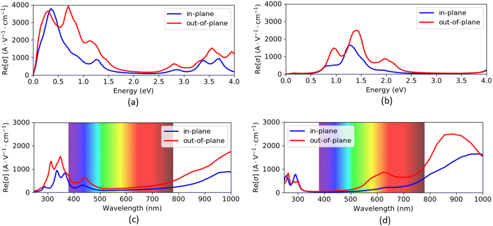 | ||
| Fig. 6 Optical conductivity as functions of energy and wavelength of VO2(B) polymorph along with in-plane and out-of-plane directions predicted by PBEsol (a and c) and PBEsol/HSE (b and d), respectively. | ||
Finally, we considered the other optical properties like refractive index (n) and extinction coefficient (k) of the VO2(B) polymorph as shown in Fig. 7, based on DFT packages PBEsol and PBEsol/HSE functionals. According to the electromagnetism theories, the complex refraction index (n) of the material corresponds to the dielectric constant based on eqn (7) and (8):
| ε1 = n2 − k2 | (7) |
| ε2 = 2nk | (8) |
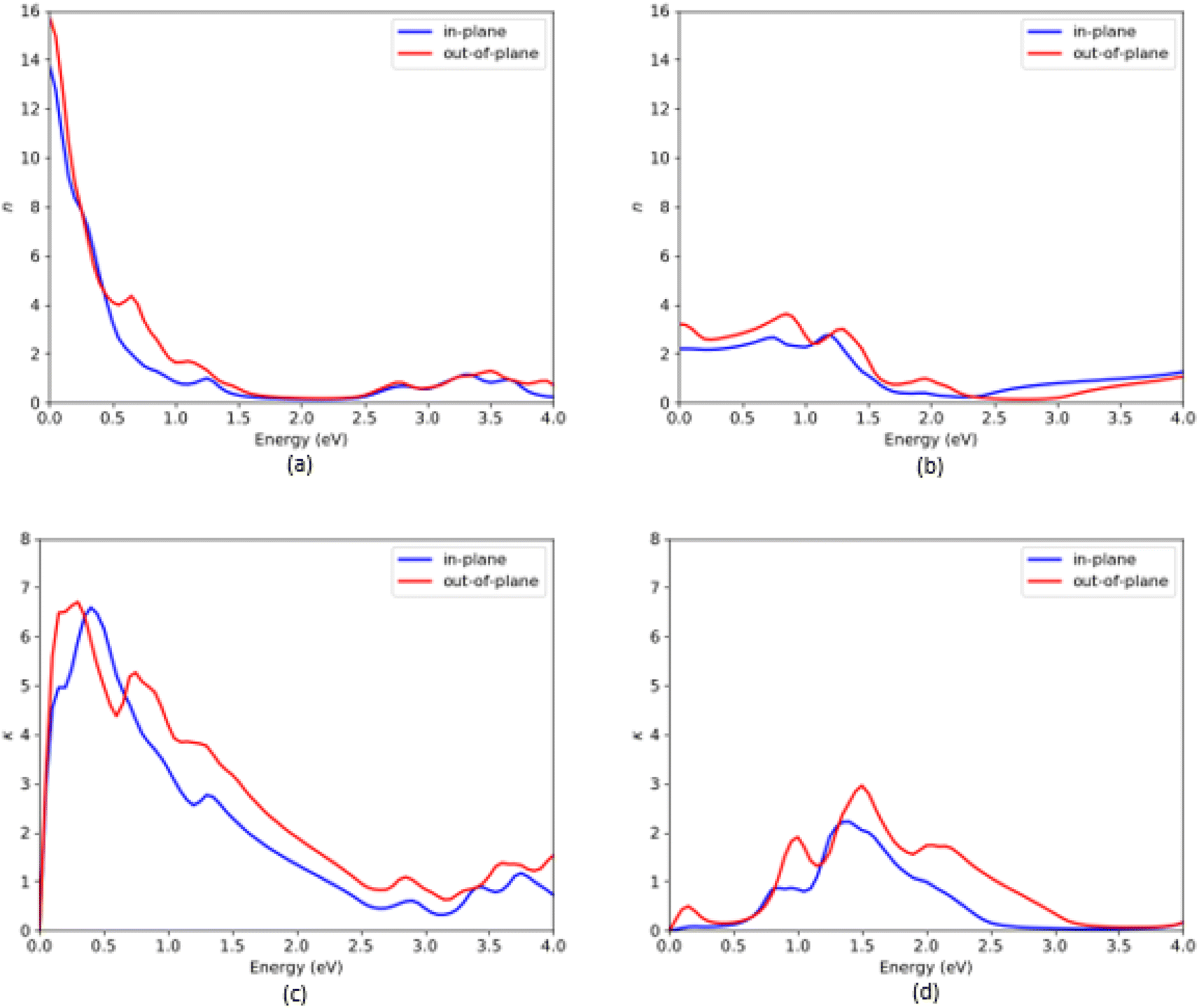 | ||
| Fig. 7 Refractive index (n) and extinction coefficient (k) of VO2(B) polymorph along with in-plane and out-of-plane directions, predicted by PBEsol (a and c) and PBEsol/HSE (b and d), respectively. | ||
As shown in Fig. 7, n and k spectra exhibit significant frequency dependent change over the entire energy range. From Fig. 7(a), the static refractive indices 2 are 13.6 and 15.7 by PBEsol, whereas the values related to the HSE calculations are 2.2 and 3.3, along the in-plane and out-of-plane directions, respectively. Moreover, the maximum values of the extinction coefficients are about 6.7/6.75 and 0.1/0.5 along with the in-plane/out-of-plane polarization directions when the system were predicted with PBEsol and HSE functionals, respectively. From the plot Fig. 7(d) related to HSE approximation, we can see other high intense peaks in the energy region 0.75–2.5 eV with the extinction coefficients 0.9 and 2.4 along the in-plane and 2.0 and 3.1 along the out-of-plane polarization directions, respectively.
Conclusions
In this study, structure, stability, electronic, and optical properties of VO2(B) polymorph have been investigated using DFT calculations. The geometrical analysis of the nanostructure based on PW basis set and GGA/PBEsol XC functional, indicated a very good consistency of V–V and V–O bond distances in the 3D structure of VO2(B) in comparison with the previous experimental and theoretical studies. The Raman spectra verified correctly the experimental observations with the Raman modes situated at 144, 185, 246, 310, 370, 507, 624 and 790 cm−1. To check the geometrical and dynamical stability of VO2(B), we calculated the cohesive energy and phonon band structure for this polymorph. The results revealed that the geometrical stability of VO2(B) with cohesive energy of −7.22 eV per atom; however, the phonon dispersion curves shown the metastability of this structure with negative acoustic modes as underlined in some experiments before. To treat the electronic and optical properties, GGA/PBEsol calculations combined with HSE hybrid functional have been performed; the latter approach requires high computational resources and large memory requirements. The electronic band structure results indicated the band gaps of 0.24 eV and 0.67 eV, according to PBEsol and PBEsol/HSE approximations, leading to metal-like and semiconductor characteristics of this polymorph in a good agreement with Lourembam et al.17 experiments. In addition, we evaluated the optical properties including the optical absorption spectra, optical conductivity, reflective index and extinction coefficient for the in-plane and out-of-plane polarizations direction for VO2(B) polymorph. The absorption coefficient and optical conductivity of this polymorph at Infrared wavelength range. The discovery of semiconducting feature associated with perfect adsorption in the IR region in the electromagnetic light of VO2(B) structure has opened a new area in electronics and photoelectronics industry. Many of these advantages were previously applied in high-performance uncooled infrared photodetector,48 dielectrics,49 microbolometers,50 as well as practical design IR heat shielding smart windows.51 Finally, we explicitly address the practice of tuning the physical properties of materials by adapting the PBEsol and HSE hybrid functionals, since out respective results were found to be very efficient for the materials characterization.Author contributions
Conceptualization, E. M., E. L. and P. S.; methodology, E. M. and E. L.; validation, E. M., E. L. and P. S; investigation, E. M.; data curation, E. M.; writing—original draft preparation, E. M.; writing—review and editing, E. M., E. L., E. P. and P. L. S.; visualization, E. M.; supervision, P. S.; project administration, E. M., E. L., P. S., L. P. and D. M. All authors have read and agreed to the published version of the manuscript.Conflicts of interest
There are no conflicts to declare.Acknowledgements
This work is part of the research of H2020 (FETPROACT-EIC-05-2019) “Nanomaterials enabling smart energy harvesting for next-generation Internet-of-Things” (NANO-EH) (grant agreement No. 951761). We also like to thank CINECA-HPC ISCRA MARCONI-100 computer system (NANO-PR project n. HP10CK3EZ0) for the calculations on QE.References
- M. Imada, A. Fujimori and Y. Tokura, Rev. Mod. Phys., 1998, 70, 1039 CrossRef.
- A. M. N. F. Zylbersztejn and N. F. Mott, Phys. Rev. B: Solid State, 1975, 11, 4383 CrossRef.
- D. Ruzmetov, S. D. Senanayake, V. Narayanamurti and S. Ramanathan, Phys. Rev. B: Condens. Matter Mater. Phys., 2008, 77, 195442 CrossRef.
- A. N. Hattori, A. I. Osaka, K. Hattori, Y. Naitoh, H. Shima, H. Akinaga and H. Tanaka, Crystals, 2020, 10, 631 CrossRef.
- T. Huang, L. Yang, J. Qin, F. Huang, X. Zhu, P. Zhou, B. Peng, H. Duan, L. Deng and L. Bi, Opt. Mater. Express, 2016, 6, 3609–3621 CrossRef CAS.
- S. R. Popuri, A. Artemenko, R. Decourt, M. Josse, U. C. Chung, D. Michau, M. Maglione, A. Villesuzanne and M. Pollet, J. Phys. Chem. C, 2015, 119, 25085–25092 CrossRef CAS.
- L. Pellegrino, N. Manca, T. Kanki, H. Tanaka, M. Biasotti, E. Bellingeri, A. S. Siri and D. Marré, Adv. Mater., 2012, 24, 2929–2934 CrossRef CAS.
- T. Sasaki, H. Ueda, T. Kanki and H. Tanaka, Sci. Rep., 2015, 5, 1–7 Search PubMed.
- J. Zhou, Y. Gao, Z. Zhang, H. Luo, C. Cao, Z. Chen, L. Dai and X. Liu, Sci. Rep., 2013, 3, 1–5 Search PubMed.
- Y. Zhang, X. Wang, Y. Zhou, H. Lai, P. Liu, H. Chen, X. Wang and W. Xie, Nano Lett., 2021, 121, 161104 Search PubMed.
- K. Li, M. Li, C. Xu, Y. Luo and G. Li, J. Alloys Compd., 2020, 816, 152655 CrossRef CAS.
- S. R. Popuri, A. Artemenko, C. Labrugere, M. Miclau, A. Villesuzanne and M. Pollet, J. Solid State Chem., 2014, 213, 79–86 CrossRef.
- Y. Oka, T. Yao, N. Yamamoto, Y. Ueda and A. Hayashi, J. Solid State Chem., 1993, 105, 271–278 CrossRef.
- M. S. Kang, S. K. Park, P. Nakhanivej, K. H. Shin, J. S. Yeon and H. S. Park, J. Alloys Compd., 2021, 855, 157361 CrossRef.
- X. Xiao, S. Li, H. Wei, D. Sun, Y. Wu, G. Jin, F. Wang and Y. Zou, J. Mater. Sci.: Mater. Electron., 2015, 26, 4226–4233 CrossRef.
- B. Guo, D. Wan, A. Ishaq, H. Luo and Y. Gao, J. Alloys Compd., 2017, 715, 129–136 CrossRef.
- J. Lourembam, A. Srivastava, C. La-o-Vorakiat, L. Cheng, T. Venkatesan and E. E. Chia, Sci. Rep., 2016, 6, 1–7 CrossRef.
- D. Wan, P. Xiong, L. Chen, S. Shi, A. Ishaq, H. Luo and Y. Gao, Appl. Surf. Sci., 2017, 397, 30–39 CrossRef.
- S. Zhang, B. Shang, J. Yang, W. Yan, S. Wei and Y. Xie, Phys. Chem. Chem. Phys., 2011, 13, 15873–15881 RSC.
- A. Srivastava, H. Rotella, S. Saha, B. Pal, G. Kalon, S. Mathew, M. Motapothula, M. Dykas, P. Yang, E. Okunishi and D. D. Sarma, APL Mater., 2015, 3, 026101 CrossRef.
- X. J. Wang, H. D. Li, Y. J. Fei, X. Wang, Y. Y. Xiong, Y. X. Nie and K. A. Feng, Appl. Surf. Sci., 2001, 177, 8–14 CrossRef.
- S. Lee, T. L. Meyer, C. Sohn, D. Lee, J. Nichols, D. Lee, S. S. A. Seo, J. W. Freeland, T. W. Noh and H. N. Lee, APL Mater., 2015, 3, 126109 CrossRef.
- P. Giannozzi, S. Baroni, N. Bonini, M. Calandra, R. Car, C. Cavazzoni, D. Ceresoli, G. L. Chiarotti, M. Cococcioni, I. Dabo and A. Dal Corso, J. Phys.: Condens. Matter, 2009, 21, 395502 CrossRef PubMed.
- S. Smidstrup, T. Markussen, P. Vancraeyveld, J. Wellendorff, J. Schneider, T. Gunst, B. Verstichel, D. Stradi, P. A. Khomyakov, U. G. Vej-Hansen and M. E. Lee, J. Phys.: Condens. Matter, 2019, 32, 015901 CrossRef.
- P. Hohenberg and W. Kohn, Phys. Rev., 1964, 136, B864 CrossRef.
- W. Kohn and L. J. Sham, Phys. Rev., 1965, 140, A1133 CrossRef.
- P. E. Blöchl, Phys. Rev. B: Condens. Matter Mater. Phys., 1994, 50, 17953 CrossRef.
- J. P. Perdew, A. Ruzsinszky, G. I. Csonka, O. A. Vydrov, G. E. Scuseria, L. A. Constantin, X. Zhou and K. Burke, Phys. Rev. Lett., 2009, 102, 039902 CrossRef.
- L. Brillouin, C. R. Hebd. Seances Acad. Sci., 1930, 191, 292 Search PubMed.
- D. Vanderbilt, Phys. Rev. B: Condens. Matter Mater. Phys., 1990, 41, 7892 CrossRef PubMed.
- D. C. Liu and J. Nocedal, Math. Program., 1989, 45, 503–528 CrossRef.
- S. Baroni, S. De Gironcoli, A. Dal Corso and P. Giannozzi, Rev. Mod. Phys., 2001, 73, 515 CrossRef.
- H. J. S. Ge and M. Ernzerhof, J. Chem. Phys., 2006, 124, 219906 CrossRef.
- O. V. Sedelnikova, L. G. Bulusheva and A. V. Okotrub, J. Chem. Phys., 2011, 134, 244707 CrossRef.
- L. Yang, J. Deslippe, C. H. Park, M. L. Cohen and S. G. Louie, Phys. Rev. Lett., 2009, 103, 186802 CrossRef.
- A. Kokalj, J. Mol. Graphics Modell., 1999, 17, 176–179 CrossRef PubMed.
- B. T. Sone, R. Benoit, S. Zongo, R. Bucher and M. Maaza, Mater. Chem. Phys., 2012, 136, 358–370 CrossRef.
- M. Kang, S. W. Kim, J. W. Ryu and T. Noh, AIP Adv., 2012, 2, 012168 CrossRef.
- X. Liu, J. Zheng, X. Jing, Y. Cheng and C. Meng, Appl. Sci., 2020, 10, 2742 CrossRef.
- B. Guo, D. Wan, A. Ishaq, H. Luo and Y. Gao, J. Alloys Compd., 2017, 715, 129–136 CrossRef.
- T. T. Song, M. Yang, J. W. Chai, M. Callsen, J. Zhou, T. Yang, Z. Zhang, J. S. Pan, D. Z. Chi, Y. P. Feng and S. J. Wang, Sci. Rep., 2016, 6, 1–9 CrossRef.
- A. Francis, S. G. Abdu, A. Haruna and D. Eli, Phys. Sci. Int. J., 2016, 11, 1–9 CrossRef.
- E. Laudadio, P. Stipa, L. Pierantoni and D. Mencarelli, Crystals, 2022, 12, 90 CrossRef.
- S. A. Corr, M. Grossman, Y. Shi, K. R. Heier, G. D. Stucky and R. Seshadri, J. Mater. Chem., 2009, 19, 4362–4367 RSC.
- S. Kim, K. Kim, C. J. Kang and B. I. Min, Phys. Rev. B, 2013, 87, 195106 CrossRef.
- J. P. Perdew and M. Levy, Phys. Rev. Lett., 1983, 51, 1884 CrossRef.
- F. Wooten, Optical Properties of Solids, Academic press, 1972, pp. 42–84 Search PubMed.
- J. Hou, B. Wang, Z. Ding, R. Dai, Z. Wang, Z. Zhang and J. Zhang, Appl. Phys. Lett., 2017, 111, 072107 CrossRef.
- C. Zhu, S. Taylor, Y. Yang and L. Wang, J. Quant. Spectrosc. Radiat. Transfer, 2017, 197, 76–83 CrossRef.
- T. H. Kil, H. J. Choi, G. Lee, B. H. Lee, S. Y. Jung, R. Ning, C. Park, S. O. Won, H. J. Chang, W. J. Choi and S. H. Baek, J. Eur. Ceram. Soc., 2020, 40, 5582–5588 CrossRef.
- C. Wang, H. Xu, C. Wang, T. Liu, S. Yang, Y. Nie, X. Guo, X. Ma and X. Jiang, J. Alloys Compd., 2021, 877, 159888 CrossRef.
| This journal is © The Royal Society of Chemistry 2022 |