DOI:
10.1039/D2RA04184G
(Paper)
RSC Adv., 2022,
12, 28985-28996
Hybrid Tamm plasmon resonance excitation towards a simple and efficient biomedical detector of NaI solution
Received
6th July 2022
, Accepted 30th September 2022
First published on 11th October 2022
Abstract
This work presents a theoretical verification for the detection of Sodium iodide (NaI) solution with different concentrations in the vicinity of Tamm plasmon (TP) resonance. The proposed sensing tool is constituted of {prism/Ag/cavity/(GaN/CaF2)15/air}. The essential foundation of this study is based on the displacement of the TP resonance by varying the concentration of an aqueous solution of sodium iodide (NaI) that fills the cavity layer. The resonant TP dip is shifted downwards the shorter wavelengths with the increment of the Ag layer thickness. Nevertheless, the resonant TP dip is shifted upwards to longer wavelengths with the increment of NaI refractive index/concentration. Also, the sensitivity of the sensing tool decreases with the increment of the NaI refractive index. However, the minimum result is not less than the value of 9913 nm RIU−1 for a concentration of 25%. Finally, the performance of our sensor in the form of the quality factor, detection limit, and figure of merit showed significant improvements in designing a high-performance liquid and biosensor.
1. Introduction
The scientific and industrial communities are always working on the design and fabrication of stable and reliable sensing devices applicable for monitoring many physical, biological, and chemical phenomena. In recent years, optical-based sensors received considerable attention as a result of their low cost, high levels of safety and also high efficiency. In this regard, these types of sensors are mainly designed and fabricated based on the changes in optical characteristics such as reflectivity, transmittivity and absorbance.1 These changes could be generated as a result of specific chemical, physical or biological characteristics. Therefore, many of the complex interactions could be simply analyzed and clarified using these simple instruments.
In this context, the excitation of Tamm plasmon (TP) resonance at the interface between a thin metallic layer of definite thickness and a multilayer periodic structure like photonic crystals (PCs) could be the mainstay for the above-mentioned sensors.1–5 Hence, PCs as artificial periodic designs in one, two, or three dimensions are capable of the formation of some stop frequency bands along the spectrum of the incident electromagnetic waves.6–8 These bands are likely defined as photonic band gaps (PBGs).6–10 In addition, PCs with a broken periodicity have significant progress through the process of photon localization.11,12 Thus, the appearance of the PBGs and photon localization grants PCs more sparkle to be the mainstay in many different applications. PCs are designed and fabricated for optical switches and reflectors,13–15 communication systems,16,17 camouflage,18 renewable energy and solar cells,19–25 and chemical, physical, and biomedical sensors.26–32 However, the transmittivity of PC structures including resonant peaks has a limited response to the variations of some physical, chemical, or biological parameters like temperature, pressure, and concentration. Therefore, the creation of TP resonance through PC designs could offer a significant response to this limited response. In particular, TP resonance is characterized by a relatively high sensitivity against any biological, physical, or chemical variations. Meanwhile, the presence of wide PBGs leads to some flexibility in the creation of TP resonance modes without any coupling with other resonant modes.33–35 In this regard, the excitation of TP resonance modes based on PC structures received considerable attention on both theoretical and experimental levels.1,33–40 In this research, we intend to present a theoretical verification for the detection of NaI solution with different concentrations in the vicinity of TP resonance. Also, this research study is introduced for sensing NaI concentrations due to the significant importance of NaI in many fields. Notably, NaI is of great potential interest through nuclear medicine diagnostics.41 Meanwhile, NaI has a significant role in the scintigraphy and therapy of the thyroid gland beside the biosynthesis of thyroid hormone.42 In addition, the treatment of iodine deficiency due to poor nutrition could be investigated using a solution of NaI mixture.41–43 For the monitoring of NaI, we have designed a cavity layer between a thin layer of Ag and a one-dimensional PC structure. Then, the suggested design is enclosed by a prism on its top surface to enhance the total reflection through the design and a substrate from the air on its bottom surface. Therefore, the proposed sensing tool is constituted as, {prism/Ag/cavity/(GaN/CaF2)15/air}. The essential foundation of this study is based on the displacement of TP resonance modes by changing the aqueous NaI concentrations through the cavity layer. Firstly, the cavity layer is filled with the pure water solution, so the TP resonance mode appears at a specific wavelength. As the water solution inside the cavity is replaced with NaI solution with different concentrations, the TP resonant mode will be displaced to new wavelengths. Therefore, the detection of NaI could be investigated relative to the shift in TP resonance positions. The numerical results are demonstrated in the vicinity of the transfer matrix method (TMM). For the best possible performance of this sensing tool, a wide optimization procedure for the thicknesses of the cavity and Ag layers and angle of incidence is investigated.
2. Sensor design and theoretical analysis
In what follows, we describe the suggested design of our proposed sensor. Fig. 1 shows the schematic representation of this sensor in which the cavity layer of a definite thickness (db) is dipped in between a thin layer of Ag metal with the thickness (da) and a one-dimensional PC structure. Here, the one-dimensional PC structure contains 15-unit cells each of them composed of gallium nitride (GaN) and calcium fluoride (CaF2) with thicknesses (dc) and (dd), respectively. Then, a prism and substrate from the air are surrounding the proposed design.
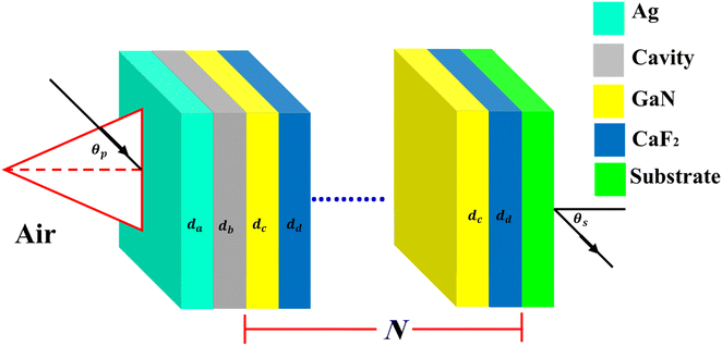 |
| | Fig. 1 The suggested design of NaI sensor that constituted as, {prism/Ag/cavity/(GaN/CaF2) 15/air substrate}. | |
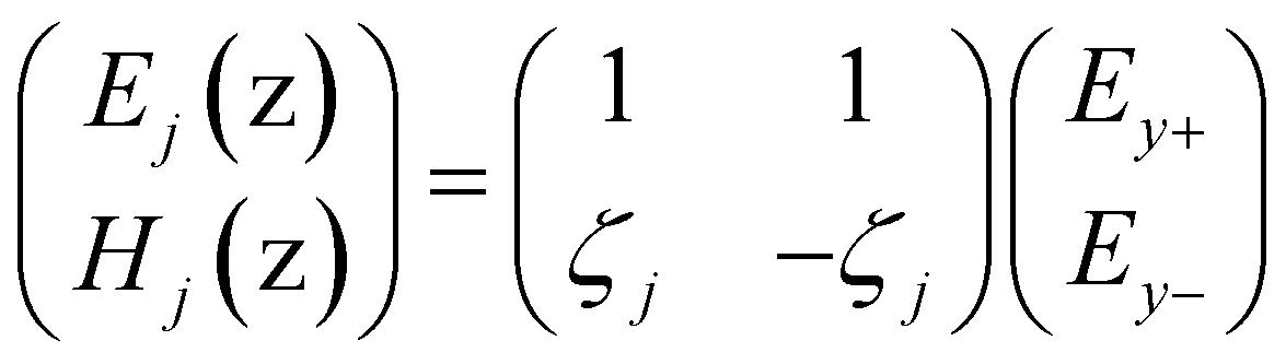
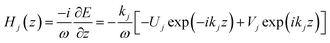
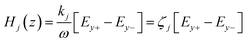
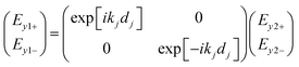
To simulate the route of the incident electromagnetic waves through the suggested design, the Transfer Matrix Method (TMM) is used. In fact the TMM is investigated to describe the response of the electric and magnetic fields through the multilayer structures as a function of the wave vector, refractive indices, and thicknesses of the constituent materials.44–46 Then, the result of this perception appears in the form of a 2 × 2 matrix. Finally, the optical characteristics of the designed structure such as transmittivity and reflectivity could be obtained in the vicinity of the basic elements of this matrix. In this regard, through a given direction (Z) as the direction of propagation, the electric and magnetic field's components for the TE mode of polarization are described as:44–46
| |
Ej(z) = Uj![[thin space (1/6-em)]](https://www.rsc.org/images/entities/char_2009.gif) exp(−ikjz) + Vjexp(ikjz) = Ey+ + Ey− exp(−ikjz) + Vjexp(ikjz) = Ey+ + Ey−
| (1a) |
| |
 | (1b) |
With

to define the wave vector component along the
Z direction as a function of the incident angle (
θj), the refractive index (
nj) and the wavelength of the incident radiation (
λ), then,
Uj and
Vj as the amplitudes of the fields components. Now
eqn (1b) can be written in a more generalized form in the vicinity of
eqn (1a) as:
| |
 | (2) |
Then, the combination of eqn (1) and (2) can lead to the following matrix formalism:
| |
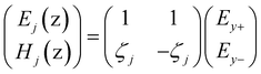 | (3a) |
With,
| |
 | (3b) |
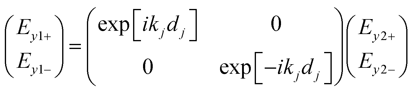
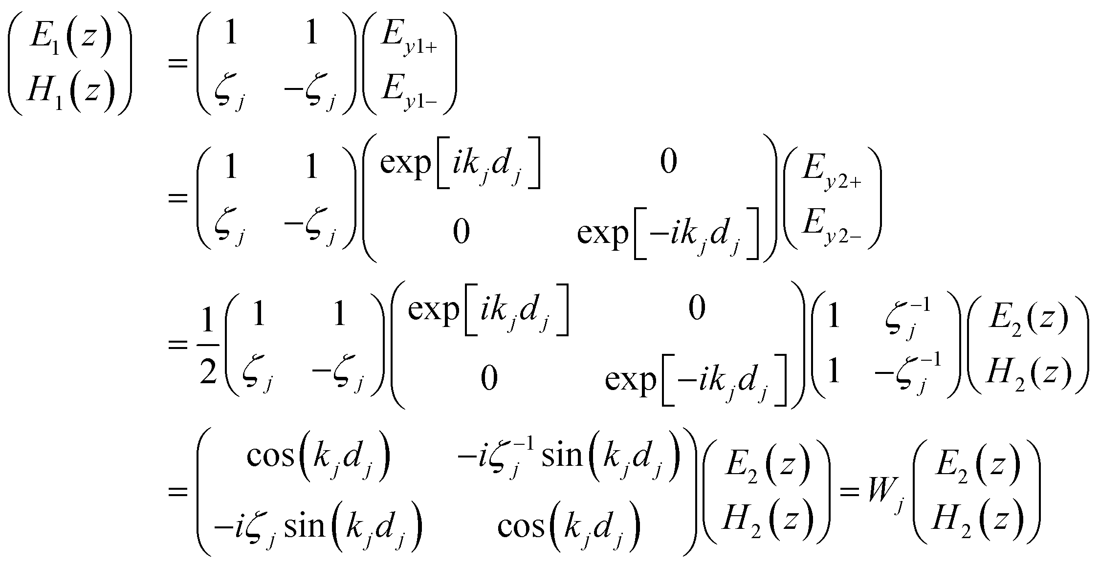
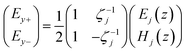
By applying eqn (3) through a distinct layer j of the designed sensor whose thickness is described as, thickness dj = Z2 − Z1, the response of the electric and magnetic fields through the upper and lower surfaces of this layer are given as,
| |
 | (4) |
Then, by substituting eqn (4) into eqn (3), we have:
| |
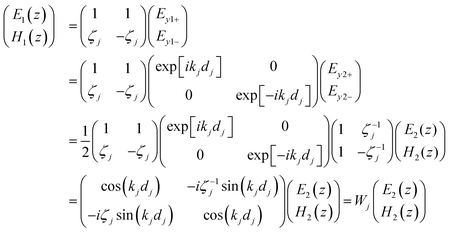 | (5) |
Here,
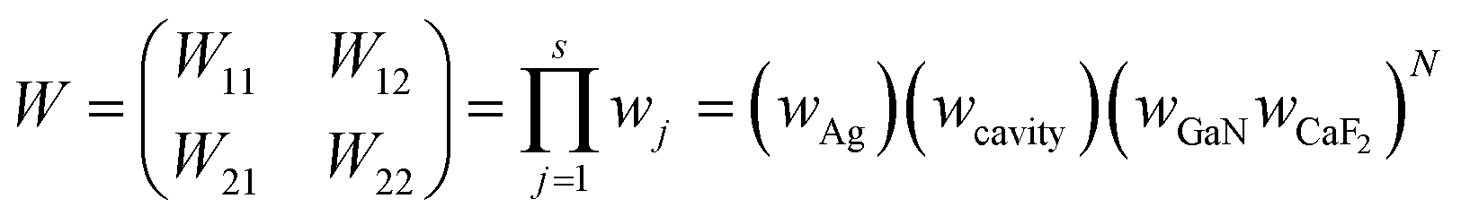
Wj describes the characteristic matrix of a distinct layer
j that defines the electric and magnetic field components through this layer. Therefore, the matrix that governs the interaction of the electromagnetic waves through the whole designed structure is given as a product of the matrices regarding each constituent layer as:
| |
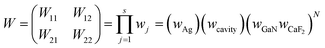 | (6) |
Such that, W11, W12, W21 and W22 are the elements of the matrix that governs the interaction between our designed sensor and the incident radiation. This matrix is given as a combination of the matrices of the Ag layer, cavity layer and the periodic structure of N periods in which each unit cell contains two layers from GaN and CaF2. Therefore, the structure reflectivity could be described as:44–46
| |
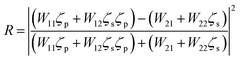 | (7) |
Here, the two coefficients
ζp =
npcos
θP and
ζs =
nscos
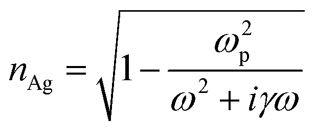
θs stand for the prism as the starting medium and substrate material, respectively. In this regard, the refractive index of the Ag layer can be expressed based on the Drude model such as:
47 | |
 | (8) |
where
ω,
ωP and
γ describe the incident frequency, the plasmon frequency of Ag, and the damping constant of Ag, respectively.
On the other side, the fabrication procedure of such a device received a significant contribution. Meanwhile, there are many previous works concerning the fabrication and study of one-dimensional photonic crystal devices.48–50 Controlling the thickness of the layers during the fabrication process of the proposed sensor is a very important point for any sensor design. For the fabrication of the design, prism/Ag/cavity/(GaN/CaF2)15/air layers, an ultra-smooth Ag layer is deposited on the prism by using the thermal evaporation technique.51 Then, a polyimide polymer film is prepared on the prism/Ag by polymerization of the m-phenylenediamine monomer. Polyimide has high heat resistance, excellent mechanical properties, and good optical transparency.52 After that, the GaN/CaF2 multilayer films are deposited on prism/Ag/polyimide. Good crystalline GaN layers can be prepared by using liquid metal gallium surface-confined nitridation reaction at room temperature.53 High optical quality CaF2 layers can be grown easily by using magnetron sputtering at low temperatures (<100 °C).54 The whole multilayer structure is now configured as prism/Ag/polyimide/(GaN/CaF2)15/air. The polyimide layer can be removed easily by chemical etching.55 Hence, the cavity in a stack of multilayers structure can be carried out for the formation of prism/Ag/cavity/(GaN/CaF2)15/air.
3. Numerical verifications and discussions
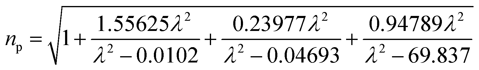
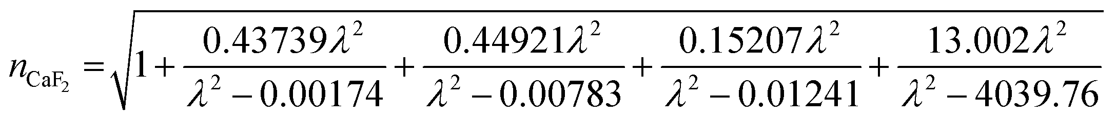
In this section, we demonstrate the numerical representations that support the dependence on the TP resonance for a relatively highly-performance sensor for NaI detection. The suggested structure is designed to show the route of the incident electromagnetic waves with wavelengths in the near IR. In the absence of the Ag cavity layer, our design is configured as {prism/cavity/(GaN/CaF2)15/air}. Here, the cavity layer with thickness = 5 μm is filled with a water solution. Also, the refractive indices of a prism (SCHOTT), GaN and CaF2 are considered based on the Sellmeier dispersions formula as the following:47,56–58 | |
 | (9) |
| |
 | (10) |
| |
 | (11) |
In addition, the cavity layer is filled with a water solution. Moreover, the thicknesses of GaN and CaF2 in each unit cell of the one-dimensional PC structure are equivalent to 100 nm and 900 nm, respectively. We can expect from eqn (10) and (11) that there is a relatively high contrast in the refractive indices of CaF2 and GaN materials. This contrast leads to the appearance of a relatively wide PBG through near IR that extends from 1436 nm to 1618 nm with 182 nm in bandwidth for the normal incidence case as shown in Fig. 2. The appearance of this PBG could be of interest in the observation of TP resonance without coupling with other dips. Furthermore, the presence of a cavity layer on the top surface of PCs does not lead to the creation of any defect modes through the PBG. Here, the absence of defect modes could be due to the large thickness of the cavity layer. In particular, the appearance of the defect mode within the PBG is strongly dependent on the quarter-wave stack condition. In another way, the formation of a defect mode through the PBG could be obtained by considering the thickness of the cavity layer in nanometers. However, the choice of this large thickness of the cavity may be preferred from a manufacturing point of view and could lead to more simplicity during the detection as well. Also, the design of the cavity layer as a cap layer on the top surface may represent a second reason.
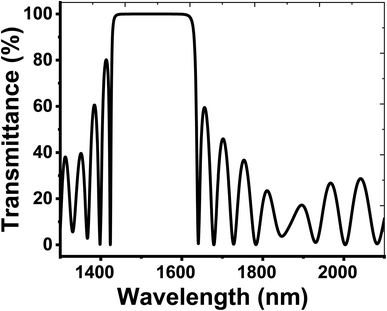 |
| | Fig. 2 The reflectivity of the suggested structure that configured as, {prism/(GaN/CaF2)15/air} in the absence of the Ag layer and for the normal incidence case. | |
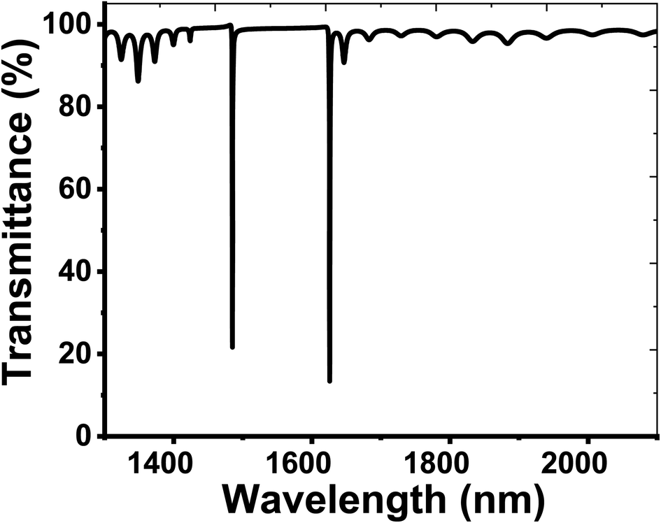
Then, by including a thin layer of Ag with thicknesses = 30 nm, the final configuration of our design becomes, {prism/Ag/cavity/(GaN/CaF2)15/air}. As mentioned before, the refractive index of the Ag layer is investigated based on Drude model for which ωp(Ag) = 1.367 × 10¹⁶ rad s−1 and γ(Ag) = 2.73 × 10¹³ rad s−1.59 Fig. 3 shows significant changes in the structure reflectivity by including Ag and cavity layers. The figure shows the formation of two reflectance dips in the wavelength's domain from 1485 nm to 1626 nm. These dips appeared in the vicinity of the PBG due to the TP resonance. The first dip is located at 1485 nm with reflectivity = 22%. Whilst the second one is observed at 1626 nm with reflectivity = 13.4%. The possible quantization of the free electrons at the interface between Ag and cavity layers represents the mainstay of the creation of TP resonance modes.60 In other words, the resonant TP dips with low group velocity come as a result of the strong coupling between the evanescent modes present in the periodic dielectric multilayer of the PC and the surface plasmon resonance in the Ag layer.61,62 These dips could be of interest through the detection procedure. However, the appearance of only one TP resonance is more preferred than the case of two dips.35,61 Usually, the appearance of more than one peak or dip is preferred in applications like filters and multiplexers.7,12,15 However, in applications like sensors, it is highly desirable for any design to adjust one peak as an indicator for the input parameter rather than two or more peaks. In addition, when the spectrum shows two peaks, sometimes this makes a conflict in determining which one is related to the change of the input parameter (like concentration, temperature, etc.). In addition, the appearance of two or more peaks through the spectrum may lead to some conflict, especially with the variation of the analyte concentration. Thus, the coincidence between two different concentrations at the same spectral wavelength due to the presence of two resonant peaks may be present. Moreover, most previous studies of different sensors adopted only one peak to determine the properties of the materials of interest.2,4,11,35
 |
| | Fig. 3 The reflectance spectrum of the suggested NaI sensor that configured as, {prism/Ag/cavity/(GaN/CaF2)15/air} for normal incidence case. | |
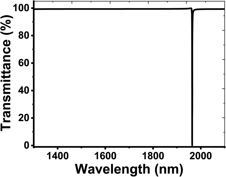
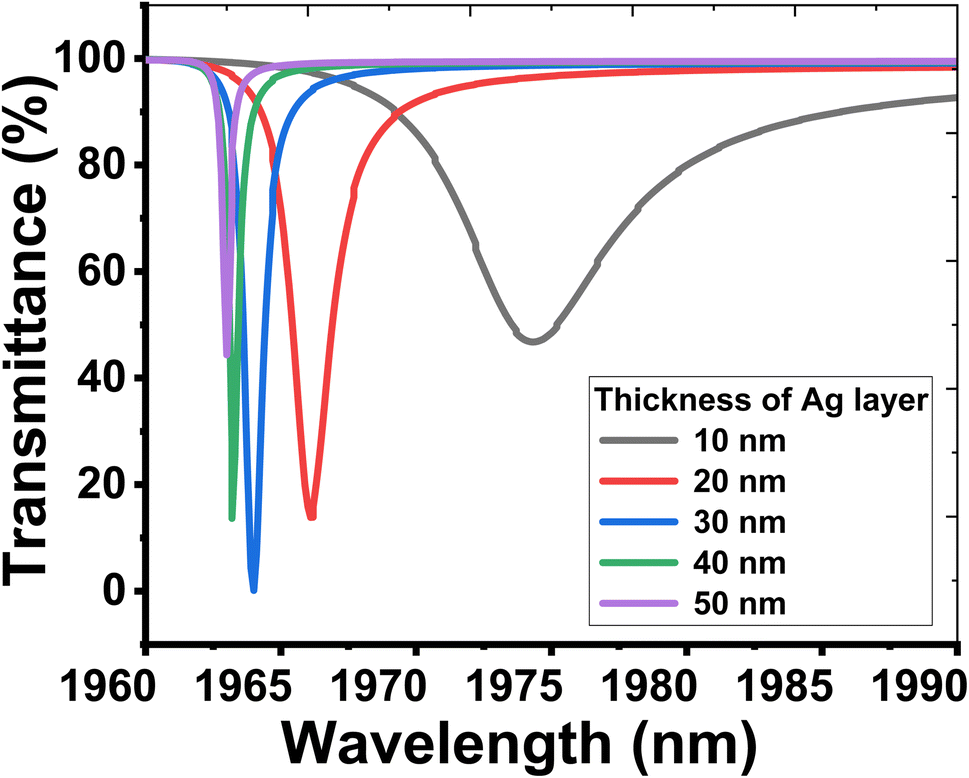
Therefore, the dependence on the effect of the angle of incidence in producing only one TP resonance mode through the reflectance spectrum could be of potential concern. After the optimization process, we investigated in Fig. 4 the appearance of only one TP resonance mode at an angle of incidence = 50° for TE polarization. The figure clarifies that the produced TP dip is located at 1964 nm with reflectivity = 0.4%. Thus, the oblique incidence for TE polarization with the angle of incidence (θp) = 50° reflects the optimum condition in our study. Physically, when the electromagnetic waves interact with our structure at θp = 50°, an evanescent mode could be produced due to the penetration of a small portion of the reflected light at the interface between the Ag layer and prism.63,64 This evanescent wave comes from the coherent oscillations of free electrons through the Ag layer relative to the alternating electric field of the incident electromagnetic radiation.65,66 In particular, the electric field associated with this evanescent wave leads to the excitation of surface plasmon waves at the interface between the cavity and Ag layers. This condition could lead to the creation of a single hybrid Tamm plasmon/surface plasmon resonance mode through the wavelengths of interest. Therefore, this dip represents the core axis during the detection procedure of NaI. Then, to complete the optimization procedure for the most possible high performance, we have discussed in Fig. 5 and 6 the optimum values for Ag and cavity layers. Fig. 5 clarifies the response of the TP resonance modes against the change in the thickness of the Ag layer. Here, the resonant TP dip is shifted downwards the short wavelengths with the increments of Ag layer thickness as shown in the figure. However, the most suitable thickness of the Ag layer that could provide a relatively high performance is investigated at 30 nm. Thus, the optimum value of the Ag layer thickness is 30 nm.
 |
| | Fig. 4 The reflectivity of the proposed design in the case of the oblique incidence for TE mode of polarization at an angle of incidence = 50°. | |
 |
| | Fig. 5 The response of TP resonance versus the change in the thickness of the Ag layer. | |
 |
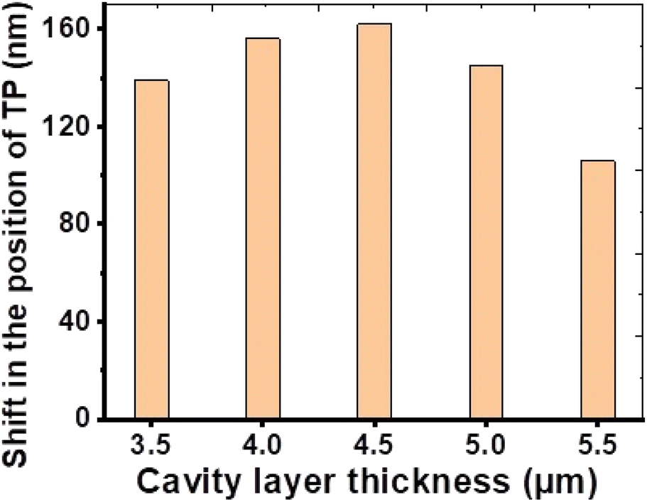
| | Fig. 6 The shift in the position of TP resonance mode relative to the variation in the cavity layer thickness from 3.5 μm to 5.2 μm. | |
In particular, the metal layer is used to support the surface plasma wave in the proposed structure. The surface plasmon resonance (SPR) can be described as a damped harmonic oscillator (DHO) driven by the electric field component of the incident light. In this context, there are many types of damping may be effective in the SPR mode such as bulk damping and surface damping. The Plasmon-damping rate can be extracted from the resonance linewidth.67 The low loss in the energy of plasma waves is desirable for many plasmonic devices such as sensing, imaging, and spectroscopy. Minimizing loss of plasmonic metal is a critical parameter for strong confinement and thus high-quality SPR. For highly damped plasmons, the plasmon wave may be vanish and the SPR mode is lossy because of the oscillations dying out. The Ag has the lowest bulk-damping coefficient compared with other plasmonic metals in the optical range due to the imaginary component of its dielectric function being very small. The strong coupling of the external optical field with the plasmon wave (photon–electron interaction) suppressed the electron energy loss.68 Therefore, optimizing the Ag thickness allows the maximum transfer of energy from the light beam to the plasmon wave, which generates the highest coupling between the plasmon wave and the evanescent wave. There is a high oscillating strength of free electrons at the optimum Ag thickness with narrow bandwidth. The reduction of the oscillating strength of plasma electrons due to damping (plasmon decay via coupling with the radiation field) is correlated to the increase of the linewidth of the peak. Hence, the excellent coupling reduces the electron energy loss and the width of the peak due to the effect of damping, which makes the proposed structure more suitable for sensor applications.
Then, to include the optimum thickness of the cavity layer, we replaced the water in the cavity with NaI solution. Meanwhile, the refractive index of NaI solution is fitted based on some experimental data at 23 °C according to the following equation:69
| | |
nNaI = 1.335 + 0.09511C + 0.2425C2
| (12) |
where
C represents the concentration of NaI through a water solution. Thus, we obtained in
Fig. 6 the optimum thickness of the cavity layer relative to the change in the concentration of NaI solution from 0 to 10%. The figure discusses the sensor sensitivity in the form of the shift that occurred for the TP mode with the change in the cavity layer thickness from 3.5 μm to 5.2 μm. At 4.5 μm, a maximum shift of 162 nm in the position of the TP resonance mode is obtained due to the change in NaI concentrations from 0 to 10%. Therefore, the optimum thickness of the cavity layer is considered at 4.5 μm through this study. In this context, we have discussed the performance of our proposed sensor based on this optimum condition in which the angle of incidence = 50° and the thicknesses of Ag and cavity layers are 30 nm and 4.5 μm, respectively.
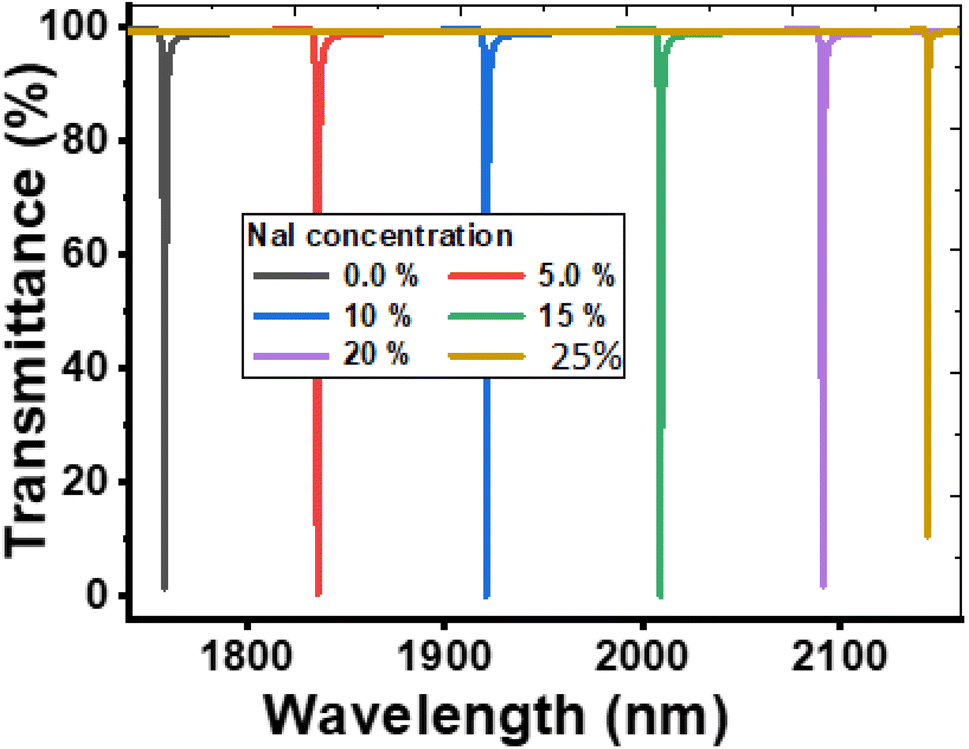
Now, Fig. 7 reflects the shift in the position of TP resonance mode due to the variations in the concentration of NaI solution from 0 to 25%. The figure shows that the resonant dip is shifted upwards the longer wavelengths with the variation of NaI concentration. As the concentration changes from 0 to 5, 10, and 15%, the reflectance dip is shifted from 1758.1 nm to 1835.5 nm, 1920.8 nm, and 2008.7 nm, respectively. For further increase in NaI concentration to 20 and 25%, the TP resonance is still shifted upwards to 2090.7 nm and 2182.1 nm, respectively. Moreover, the reflectivity of the resonant dip is almost constant, especially at concentrations smaller than 20%. Here, the shift of the resonant dip results due to the change in the optical path length with the increase of NaI concentrations. In this context, at constant thicknesses of the constituent materials and the angle of incidence, the wavelength of the TP resonance mode increases to match the increase in the refractive index of NaI as a result of the increase in its concentration.70,71 This scenario leads to the verification of a constant phase condition (φc = 2πnbdbcos(θb)/λ).71
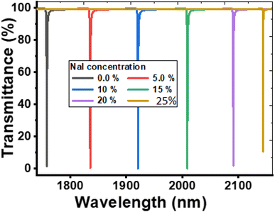 |
| | Fig. 7 The shift in the TP resonance mode relative to the change in the concentration of NaI solution. | |
In the midst of the investigated results in Fig. 7, we present in Table 1 the parameters that highlight the performance of the proposed NaI sensor. Table 1 indicates the performance of our sensor in the vicinity of calculating the sensitivity (S), quality factor (QF), detection limit (DL) and figure of merit (FoM). These parameters are calculated based on the following relations:72–75
| |
 | (13a) |
| |
 | (13b) |
| |
 | (13c) |
| |
 | (13d) |
Table 1 Sensitivity (S), quality factor (QF), detection limit (DL) and figure of merit (FoM) values of the proposed NaI sensor
| C (%) |
nNaI |
λTP (nm) |
Intensity (%) |
FWHM (nm) |
S (nm RIU−1) |
QF |
DL × 10−6 |
FoM |
| 0.0 |
1.335 |
1758.10 |
1.35 |
1.04 |
— |
1688.67 |
— |
— |
| 5.0 |
1.3404 |
1836.04 |
0.54 |
1.02 |
14433.38 |
1787.73 |
3.56 |
14053.66 |
| 10 |
1.3469 |
1920.79 |
0.09 |
0.99 |
13672.11 |
1922.89 |
3.65 |
13687.03 |
| 15 |
1.3547 |
2008.71 |
0.14 |
0.96 |
12721.56 |
2070.96 |
3.81 |
13115.83 |
| 20 |
1.3637 |
2090.70 |
1.89 |
0.78 |
11589.07 |
2661.86 |
3.39 |
14755.07 |
| 25 |
1.3739 |
2143.72 |
10.51 |
0.31 |
9913.30 |
6902.78 |
1.57 |
31920.74 |
Such that, λTP describes the wavelength of the TP resonance mode, ΔλTP indicates the shift in the position of TP mode and FWHM describes the full width at the half maximum of the TP resonance mode.
Finally, we have graphically considered the performance of our sensor as indicated in Fig. 8–13 based on the numerical results in Table 1. Fig. 8 shows the change in the position of the TP mode regarding the change in the refractive index of the NaI solution. The figure shows that the position of the resonant TP dip is shifted upwards the longer wavelengths as the refractive index of NaI increases. In general, the resonant TP dip is shifted from 1758.1 nm to 2143.73 nm due to the change in NaI concentration from 0.0 to 25%. This change could be described by the quadratic fitting of the numerical results in Fig. 8 according to the following equation:
| | |
λTP = −148038n2NaI + 411024nNaI − 283123, R2 = 0.9997
| (14) |
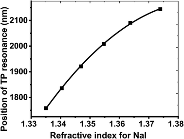 |
| | Fig. 8 The position of TP resonance as a function of refractive index for NaI solution. | |
 |
| | Fig. 9 The sensitivity of the proposed sensing tool versus the change in the refractive index of NaCl solution. | |
 |
| | Fig. 10 The change in the values of FWHM of TP resonance with the variations in the refractive index of NaI solution. | |
 |
| | Fig. 11 The dependence of QF on the refractive index of NaI solution. | |
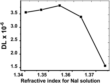 |
| | Fig. 12 The detection limit of the proposed sensor with respect to the change in the refractive index of the NaI solution. | |
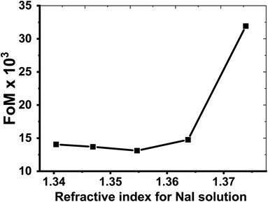 |
| | Fig. 13 The response of the figure of merit versus the refractive index of NaI solution. | |
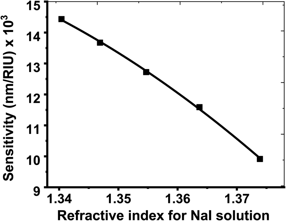
Therefore, at a specified value of λTP, both the refractive index and concentration of NaI could be obtained based on eqn (12) and (14). Then, Fig. 9 describes the sensitivity of our sensing tool versus the variation in the refractive index of NaI. The figure shows that the sensitivity decreases with the increase of the NaI refractive index. However, the value is still exceeding 9913 nm RIU−1. This response could be described in the vicinity of the following fitted equation:
| S = 2 × 10⁶(nNaI − 1) − 944654n2NaI, R2 = 0.999415 |
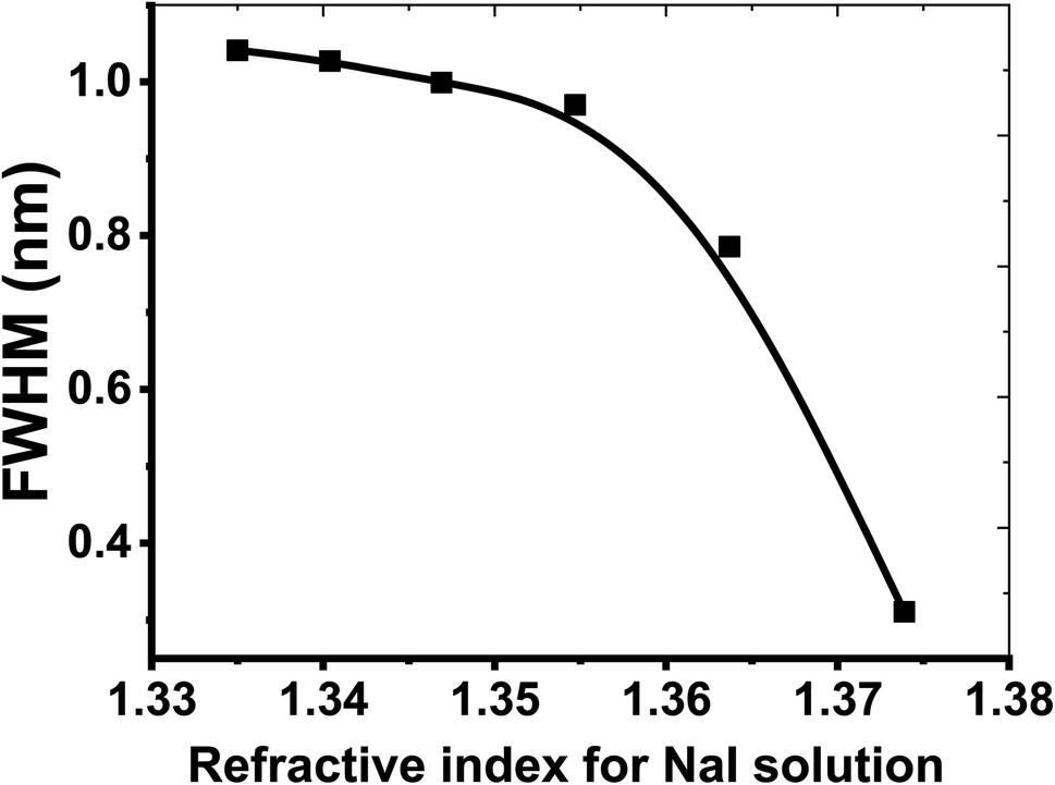
After that, we discussed in Fig. 10 the response of the FWHM of TP resonance versus the change in the refractive index of NaI solution. The figure indicates that the FWHM is slightly decreasing with the increase of the refractive index, especially at nNaI smaller than 1.3547. Then, a sharp decrease could be investigated at larger values. Here, the decrease in FWHM leads to a sharp profile of the TP resonance mode. In this regard, the plasmon resonance of metal is sensitive to its surrounding environment (local refractive index). Therefore, the damping rate depends on the interface between the Ag layer and NaI solution.76 This is due to the adsorption of NaI molecules on the Ag surface which affects the polarizability and propagation of the plasmonic wave. This type of damping is called chemical interface damping (CID).77 The chemical interface damping (CID) refers to the observation that the same Ag layer in different chemical environments displays differences in the plasmon line width. Hence, the refractive index of the NaI solution plays an important role in the linewidth of the resonance mode. The NaI solution is polarized in response to the resulting electric field of the plasmon wave. In addition, the polarization of materials is determined by the dielectric function. The imaginary part of the dielectric function for NaI salt is almost zero over the wavelength range 1700–2200 nm and so the NaI solution is considered lossless.
With increasing the refractive index (concentration) of the NaI solution, the permittivity and polarizability of the NaI solution will increase. A material with high permittivity polarizes more in response to an applied electric field than a material with low permittivity, thereby storing more energy in the material. This leads to accelerating the resonance energy transfer from the Ag layer into GaN/CaF2 multilayer films, and consequently decreasing the loss and lowering FWHM. Thus, the performance of our sensor in the form of the quality factor, detection limit and figure of merit is expected to provide significant improvements.
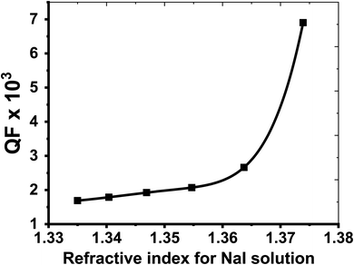
Then, we plotted in Fig. 11 the dependence of the quality factor on the refractive index of the NaI solution. The figure indicates that the values of QF increase with the increase of the NaI index, especially at nNaI larger than 1.3547. This response could be understood in the vicinity of eqn (13b) and Fig. 10 as a result of the strong dependence of QF on the values of FWHM. Meanwhile, the maximum value of QF (6902) is investigated at nNaI = 1.3739 (relative to a concentration of NaI = 25%) in which the smallest value of FWHM is obtained. Moreover, the dependence of QF on the index of NaI according to the fitting of the numerical results as:
| | |
QF = 2 × 10¹¹n5NaI − 1 × 10¹²n4NaI + 4 × 10¹²n3NaI − 5 × 10¹²n2NaI + 4 × 10¹²nNaI − 9 × 10¹¹, R2 = 1
| (16) |
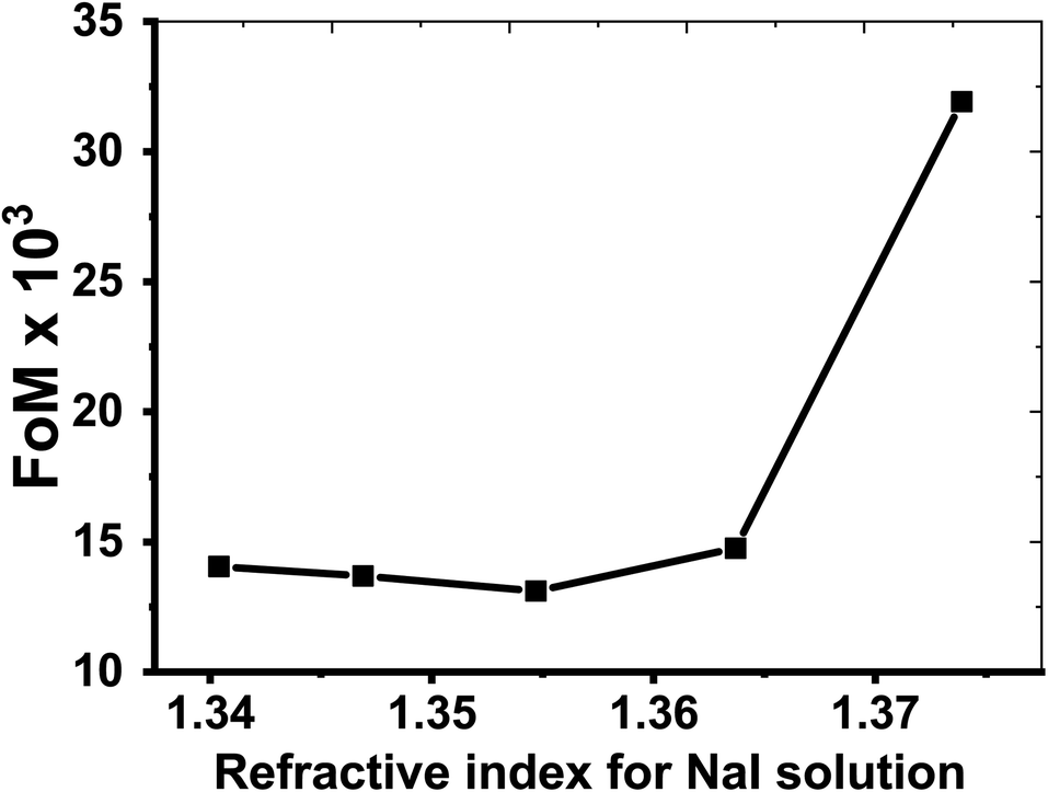
Then, Fig. 12 and 13 clarify the response of DL and FoM, respectively against the refractive index of NaI solution. Fig. 12 provides relatively small values of DL that decrease with the increase of the NaI refractive index. In this context, our sensor could receive a DL of 0.157 × 10⁻⁶ that supports the efficient performance of this sensor. In addition, the figure of merit increases with the refractive index due to the decrease in the values of FWHM as shown in Fig. 13. Here, our sensor provides a value of FoM over 31900.
Finally, the investigated results could be of interest towards considering our proposed sensor as a promising platform for NaI detection and sensing. In particular, Table 2 supports this idea compared to its counterparts in optical, photonic and phononic devices.78–83
Table 2 The performance of the proposed sensor in the form of sensitivity versus some optical and photonic ones
| Ref. |
The designed structure |
Sensing materials |
Sensitivity (nm RIU−1) |
| 78 |
Photonic crystal cavity sensor |
Sodium chloride (NaCl) solution |
428 |
| 79 |
Two-core optical fiber |
NaCl solution |
1400 |
| 80 |
Two-core optical fiber |
Salinity |
2834.3 |
| 81 |
Tri-core photonic crystal fiber |
Salinity and temperature |
5674 |
| 82 |
Fabry–Pérot interferometer |
Temperature |
6830 |
| 83 |
Two-dimensional solid–liquid phononic crystal |
NaI–water concentrations |
1714 |
| 35 |
1D porous silicon photonic crystal fluid sensor based on TP resonance |
Different fluids |
5018 |
| 46 |
1D photonic crystal as a gas sensor based on TP resonance |
Toluene |
273 |
| 84 |
Experimental gas sensor based on TP resonance |
Organic vapors |
70 |
| 85 |
Metallo-dielectric heterostructure configuration based on TP resonance |
Different liquids |
970 |
| 86 |
Theoretical gas sensor using photonic crystal cavity based on TP resonance |
Methane gas |
450 |
| Our design |
[prism/Ag/NaI cavity/(GaN/CaF2)15/Air] |
Sodium iodide |
14433 |
4. Conclusions
In this work, we proposed a PC design with the configuration {prism/Ag/cavity/(GaN/CaF2)15/air} as a highly sensitive tool for the detection of NaI solution at different concentrations. Significant changes in the transmission spectra of the proposed structure were produced depending on Ag and cavity layers. The most suitable thickness of the Ag layer that could provide a relatively high performance is investigated at 30 nm. A maximum shift of 162 nm in the position of the TP resonance dip is obtained due to the change in NaI concentration from 0.0 to 10%. As the concentration changes from 0 to 05, 10%, and 0.15, the TP resonance dip is shifted from 1758.1 nm to 1835.5 nm, 1920.8 nm, and 2008.7 nm, respectively. For further increase in NaI concentration to 20 and 25%, the TP resonance dip is still shifted upwards to 2090.7 nm and 2182.1 nm, respectively. The values of QF increase with the increment of NaI refractive index, especially at nNaI larger than 1.3547. The proposed sensor is a promising platform for NaI sensor detector and sensing especially when compared with its counterparts in optical, photonic and phononic devices.
Conflicts of interest
The authors declare they have no conflicts of interests.
Acknowledgements
This work was funded by the Deanship of Scientific Research at Jouf University under grant No (DSR-2021-03-0308).
References
- J. Morrone, J. I. Ramallo, D. F. Lionello, A. Zelcer, B. Auguié, P. C. Angelomé and M. C. Fuertes, Incorporation of porous protective layers as a strategy to improve mechanical stability of Tamm plasmon based detectors, Mater. Adv., 2021, 2, 2719 RSC.
- B. Auguie, M. C. Fuertes, P. C. Angelome, N. L. Abdala, G. J. A. A. Soler Illia and A. Fainstein, Tamm Plasmon Resonance in Mesoporous Multilayers: Toward a Sensing Application, ACS Photonics, 2014, 1, 775–780 CrossRef CAS.
- M. Kaliteevski, I. Iorsh, S. Brand, R. A. Abram, J. M. Chamberlain, A. V. Kavokin and I. A. Shelykh, Tamm plasmon-polaritons: Possible electromagnetic states at the interface of a metal and a dielectric Bragg mirror, Phys. Rev. B: Condens. Matter Mater. Phys., 2007, 76, 165415 CrossRef.
- Z. A. Zaky, A. M. Ahmed, A. S. Shalaby and A. H. Aly, Refractive index gas sensor based on the Tamm state in a one-dimensional photonic crystal: Theoretical optimization, Sci. Rep., 2020, 10, 9736 CrossRef CAS PubMed.
- W. L. Zhang, F. Wang, Y. J. Rao and Y. Jiang, Novel sensing concept based on optical Tamm plasmon, Opt. Express, 2014, 22, 14524–14529 CrossRef CAS PubMed.
- J. Joannopoulos, S. Johnson and R. Meade, Photonic Crystals: Molding the Flow of Light, Princenton University Press, 2007 Search PubMed.
- E. Yablonovitch, Photonic crystals: semiconductors of light, Sci. Am., 2001, 285, 46–55 CrossRef CAS.
- J. Knight, J. Broeng, T. Birks and P. Russell, Photonic band gap guidance in optical fibers, Science, 1998, 282, 1476–1478 CrossRef CAS PubMed.
- R. Meade, A. Rappe, K. Brommer, J. Joannopoulos and O. Alerhand, Accurate theoretical analysis of photonic band-gap materials, Phys. Rev. B, 1993, 48, 8434 CrossRef CAS PubMed.
- C. L. M. Hofmann, S. Fischer, E. H. Eriksen, B. Bläsi, C. Reitz, D. Yazicioglu, I. A. Howard, B. S. Richards and J. C. Goldschmidt, Experimental validation of a modeling framework for upconversion enhancement in 1D-photonic crystals, Nat. Commun., 2021, 12, 104 CrossRef CAS PubMed.
- A. H. Aly and H. A. Elsayed, Defect mode properties in a one-dimensional photonic crystal, Physica B, 2012, 407, 120–125 CrossRef CAS.
- N. Ansari and K. Mirbaghestan, Design of Wavelength-Adjustable Dual-Narrowband Absorber by Photonic Crystals With Two Defects Containing MoS2 Monolayer, J. Lightwave Technol., 2020, 38(23), 6678–6684 CAS.
- J. Knight, T. Birks, P. Russell and D. Atkin, All-silica single-mode optical fiber with photonic crystal cladding, Opt. Lett., 1996, 21, 1547–1549 CrossRef CAS PubMed.
- T. Birks, J. Knight and P. Russell, Endlessly single-mode photonic crystal fiber, Opt. Lett., 1997, 22, 961–963 CrossRef CAS PubMed.
- H. A. Elsayed, Quasiperiodic photonic crystals for filtering purpose by means of the n doped semiconductor material, Phys. Scr., 2020, 95(6), 065504 CrossRef CAS.
- K. Hao, Y. Gao, J. Du, X. Wang, J. Zhang, S. Yang and Z. Li, One-dimensional photonic crystal transparent wall with wide-angle and polarization-insensitive for 5G signal transmission, Optik, 2021, 242, 167047 CrossRef CAS.
- M. N. E. Temmar, A. Hocini, D. Khedrouche and T. A. Denidni, Analysis and design of MIMO indoor communication system using terahertz patch antenna based on photonic crystal with graphene, Photonics Nanostruct., 2021, 43, 100867 CrossRef.
- Z. Deng, Y. Su, W. Gong, X. Wang and R. Gong, Temperature characteristics of Ge/ZnS one-dimension photonic crystal for infrared camouflage, Opt. Mater., 2021, 121, 111564 CrossRef CAS.
- H. Huang, H. Li, X. Shen, K. Gu, J. Guo and C. Wang, Gecko-inspired smart photonic crystal films with versatile color and brightness variation for smart windows, Chem. Eng. J., 2022, 429, 132437 CrossRef CAS.
- J. Krügener, M. Rienacker, S. Schafer, M. Sanchez, S. Wolter, R. Brendel, S. John, H. J. Osten and R. Peibst, Photonic crystals for highly efficient silicon single junction solar cells, Sol. Energy Mater. Sol. Cells, 2021, 233, 111337 CrossRef.
- S. Hong-jun, T. Li, L. Hui-dong, H. Xian-jian and X. Li, Enhancement of light absorption in thin film silicon solar cells with light traping, Chin. J. Lumin., 2016, 37(7), 816–822 CrossRef.
- S. Anishkumar and A. Aldrin, Tuneable and spectrally selective broad-band reflector – Modulated photonic crystals and its application in solar cells, Sol. Energy, 2018, 162, 525–532 CrossRef.
- H. A. Elsayed, H. Sayed, T. A. Taha, A. G. Alharbi, A. M. Alenad, B. A. Alshammari, A. M. Ahmed, A. Mehaney and A. H. Aly, Simple and efficient design towards a significant improvement of the optical absorption of amorphous silicon solar cell, J. Quant. Spectrosc. Radiat. Transfer, 2021, 275, 107890 CrossRef CAS.
- P. Kuang, S. Eyderman, M. L. Hsieh, A. Post, S. John and S. Y. Lin, Achieving an accurate surface profile of a photonic crystal for near-unity solar absorption in a super thin film architecture, ACS Nano, 2016, 10, 6116–6612 CrossRef CAS PubMed.
- D. I. Kim, J. W. Lee, R. H. Jeong, J.-H. Yu, J. W. Yang, S.-H. Nam and J.-H. Boo, Enhancing the optical properties using hemisphere TiO2 photonic crystal as the electron acceptor for perovskite solar cell, Appl. Surf. Sci., 2019, 487, 409–415 CrossRef CAS.
- L. Gonzalez and N. Porras-Montenegro, Pressure, temperature and plasma frequency effects on the band structure of a 1D semiconductor photonic crystal, Phys. E, 2012, 44, 773–777 CrossRef CAS.
- H. Hung, C. Wu and S. Chang, Terahertz temperature-dependent defect mode in a semiconductor-dielectric photonic crystal, J. Appl. Phys., 2011, 110, 093110 CrossRef.
- B. Vasić and R. Gajić, Graphene-Covered Photonic Structures for Optical Chemical Sensing, Phys. Rev. Appl., 2015, 4, 024007 CrossRef.
- X. Qing and M. H. Sani, Optical refractive index sensor for detection of N2, He and CO2 gases based on square resonance nanocavity in 2D photonic crystal, Opt. Commun., 2021, 490, 126940 CrossRef CAS.
- A. Bijalwan, B. K. Singh and V. Rastogi, Analysis of one-dimensional photonic crystal based sensor for detection of blood plasma and cancer cells, Optik, 2021, 226, 165994 CrossRef CAS.
- N. A. Mohammed, M. M. Hamed, A. A. M. Khalaf, A. Alsayyari and S. El-Rabaie, High-sensitivity ultra-quality factor and remarkable compact blood components biomedical sensor based on nanocavity coupled photonic crystal, Results Phys., 2019, 14, 102478 CrossRef.
- A. Panda, D. Vigneswaran, P. D. Pukhrambam, N. Ayyanar and T. K. Nguyen, Design and Performance Analysis of Reconfigurable 1D Photonic Crystal Biosensor employing Ge2Sb2Te5 (GST) for Detection of Women Reproductive Hormones, IEEE Trans. NanoBioscience, 2022, 21(1), 21–28 Search PubMed.
- K. V. Sreekanth, S. Zeng, K. T. Yong and T. Yu, Sensitivity enhanced biosensor using graphene-based one-dimensional photonic crystal, Sens. Actuators, B, 2013, 182, 424–428 CrossRef CAS.
- G. Lheureux, M. Monavarian, R. Anderson, R. A. Decrescent, J. Bellessa, C. Symonds, J. A. Schuller, J. S. Speck, S. Nakamura and S. P. DenBaars, Tamm plasmons in metal/nanoporous GaN distributed Bragg reflector cavities for active and passive optoelectronics, Opt. Express, 2020, 28, 17934–17943 CrossRef CAS PubMed.
- A. M. Ahmed and A. Mehaney, Ultra-high sensitive 1D porous silicon photonic crystal sensor based on the
coupling of Tamm/Fano resonances in the mid-infrared region, Sci. Rep., 2019, 9, 6973 CrossRef PubMed.
- N. Li, T. Tang, J. Li, L. Luo, P. Sun and J. Yao, Highly sensitive sensors of fluid detection based on magneto-optical optical Tamm state, Sens. Actuators, B, 2018, 265, 644–651 CrossRef CAS.
- M. Mehdi Keshavarz and A. Alighanbari, Self-referenced terahertz refractive index sensor based on a cavity resonance and Tamm plasmonic modes, Appl. Opt., 2020, 59, 4517–4526 CrossRef CAS PubMed.
- M. C. Sansierra, J. Morrone, F. Cornacchiulo, M. C. Fuertes and P. C. Angelome, Detection of Organic Vapors Using Tamm Mode Based Devices Built from Mesoporous Oxide Thin Films, ChemNanoMat, 2019, 5, 1289–1295 CrossRef CAS.
- Y. Tsurimaki, J. K. Tong, V. N. Boriskin, A. Semenov, M. I. Ayzatsky, Y. P. Machekhin, G. Chen and S. V. Boriskina, Topological Engineering of Interfacial Optical Tamm States for Highly Sensitive Near-Singular-Phase Optical Detection, ACS Photonics, 2018, 5, 929–938 CrossRef CAS.
- A. Juneau-Fecteau and L. G. Fréchette, Tamm plasmon-polaritons in a metal coated porous silicon photonic crystal, Opt. Mater. Express, 2018, 8(9), 2774–2781 CrossRef CAS.
- S. Ravera, A. Reyna-Neyra, G. Ferrandino, L. M. Amzel and N. Carrasco, The sodium/iodide symporter (NIS): molecular physiology and preclinical and clinical applications, Annu. Rev. Physiol., 2017, 79, 261–289 CrossRef CAS PubMed.
- D. P. Carvalho and A. C. F. Ferreira, The importance of sodium/iodide symporter (NIS) for thyroid cancer management, Arq. Bras. Endocrinol. Metabol., 2007, 51(5), 672–682 CrossRef PubMed.
- E. Darrouzeta, S. Lindenthal, D. Marcellina, J.-L. Pellequere and T. Pourcher, The sodium/iodide symporter: State of the art of its molecular characterization, Biochim. Biophys. Acta, 2014, 1838, 244–253 CrossRef PubMed.
- S. J. Orfanidis, Electromagnetic Waves and Antennas. Rutger University ( 2008) Search PubMed.
- M. Born and E. Wolf, “Principles of Optics Electromagnetic Theory of Propagation, Interference and Diffraction of Light”, Cambridge University Press Archive, ( 1999) Search PubMed.
- A. M. Ahmed, M. Ahmed and A. Hussein, Elsayed “Detection of toluene traces in exhaled breath by using a 1D PC as a biomarker for lung cancer diagnosis”, Eur. Phys. J. Plus, 2021, 136, 626 Search PubMed.
- A. Alabastri, S. Tuccio, A. Giugni, A. Toma, C. Liberale, G. Das, F. De. Angelis, E. Di. Fabrizio and R. Zaccaria, Molding of plasmonic resonances in metallic nanostructures: dependence of the non-linear electric permittivity on system size and temperature, Mater, 2013, 6, 4879–4910 CrossRef PubMed.
- H. Shen, Z. Wang, Y. Wu and B. Yang, One-dimensional photonic crystals: fabrication, responsiveness and emerging applications in 3D construction, RSC Adv., 2016, 6, 4505–4520 RSC.
- L. González-García, S. Colodrero, H. Míguez and A. R. González-Elipe, Single-step fabrication process of 1-D photonic crystals coupled to nanocolumnar TiO2 layers to improve DSC efficiency, Opt. Express, 2015, 23(24), A1642–A1650 CrossRef PubMed.
- M. Shaban, A. Ahmed, Abdel-Rahman and H. Hamdy, Tunability and Sensing Properties of Plasmonic/1D Photonic Crystal, Sci. Rep., 2017, 7, 41983 CrossRef CAS PubMed.
- B. W. Stuart, X. Tao, D. Gregory and H. E. Assender, Roll-to-roll patterning of Al/Cu/Ag electrodes on flexible poly(ethylene terephthalate) by oil masking: a comparison of thermal evaporation and magnetron sputtering, Appl. Surf. Sci., 2020, 505, 144294 CrossRef CAS.
- Ki. Fukukawa and M. Ueda, Recent Progress of Photosensitive Polyimides, Polym. J., 2008, 40, 281–296 CrossRef CAS.
- Q. Li, B.-D. Du, J.-Ye Gao, B.-Yu Xing, D.-K. Wang, Ji-F. Ye and J. Liu, Room-Temperature Printing of Ultrathin Quasi-2D GaN Semiconductor via Liquid Metal Gallium
Surface Confined Nitridation Reaction, Adv. Mater. Technol., 2022 DOI:10.1002/admt.202200733.
- N. J. Dudney, Radio frequency magnetron sputter deposition of CaF2CaF2 films, J. Vac. Sci. Technol., A, 1998, 16, 615 CrossRef CAS.
- S.-M. Lian, K.-M. Chen, R.-J. Lee, J.-P. Pan and A. Hung, Chemical etching of polyimide film, J. Appl. Polym. Sci., 1995, 58(9), 1577–1584 CrossRef CAS.
- https://www.schott.com/advanced_optics/english/download/.
- M. Daimon and A. Masumura, High-accuracy measurements of the refractive index and its temperature coefficient of calcium fluoride in a wide wavelength range from 138 to 2326 nm, Appl. Opt., 2002, 41, 5275–5281 CrossRef CAS PubMed.
- A. S. Barker Jr and M. Ilegems, Infrared lattice vibrations and free-electron dispersion in GaN, Phys. Rev. B, 1973, 7, 743–750 CrossRef.
- P. Markos and C. M. Soukoulis. Wave propagation: from electrons to photonic crystals and left-handed materials. Princeton University Press, ( 2008) Search PubMed.
- H.-P. Chiang, H.-T. Yeh, C.-M. Chen, J.-C. Wu, S.-Y. Su, R. Chang, Y.-J. Wu, D. P. Tsai and P. T. Leung, Surface plasmon resonance monitoring of temperature via phase measurement, Opt. Commun., 2004, 241, 409–418 CrossRef CAS.
- S. Amoudache, R. Moiseyenko, Y. Pennec, B. D. Rouhani, A. Khater, R. Lucklum and R. Tigrine, Optical and acoustic sensing using Fano-like resonances in dual phononic and photonic crystal plate, J. Appl. Phys., 2016, 119(11), 114502 CrossRef.
- M. Zaremanesh, L. Carpentier, H. Gharibi, A. Bahrami, A. Mehaney, A. Gueddida, R. Lucklum, B. Djafari-Rouhani and Y. Pennec, Temperature biosensor based on triangular lattice phononic crystals, APL Mater., 2021, 9, 061114 CrossRef CAS.
- S. A. Ramakrishna and A. D. Armour, Propagating and evanescent waves in absorbing media, Am. J. Phys., 2003, 71(6), 562–567 CrossRef.
- S. Kumar, G. Sharma and V. Singh, Sensitivity Modulation of Surface Plasmon Resonance Sensor Configurations in Optical Fiber Waveguide, Prog. Electromagn. Res. Lett., 2013, 37, 167–176 CrossRef.
- M. A. Basyooni, A. M. Ahmed and M. Shaban, Plasmonic hybridization between two metallic nanorods, Optik, 2018, 172, 1069–1078 CrossRef CAS.
- A. M. Ahmed and M. Shaban, Highly sensitive Au–Fe2O3–Au and Fe2O3–Au–Fe2O3 biosensors utilizing strong surface plasmon resonance, Appl. Phys. B, 2020, 126, 57 CrossRef CAS.
- K. Kolwas and A. Derkachova, Damping rates of surface plasmons for particles of size from nano- to micrometers; reduction of the nonradiative decay, J. Quant. Spectrosc. Radiat. Transfer, 2013, 114, 45–55 CrossRef CAS.
- V. B. Gildenburg, V. A. Kostin and I. A. Pavlichenko, Excitation of surface and volume plasmons in a metal nanosphere by fast electrons, Phys. Plasmas, 2016, 23, 032120 CrossRef.
- K. Bai and J. Katz, On the refractive index of sodium iodide solutions for index matching in PIV, Exp. Fluids, 2014, 55, 1704 CrossRef.
- B. Auguie, M. C. Fuertes, P. C. Angelome, N. L. Abdala, S. G. J. A. A. Illia and A. Fainstein, Tamm plasmon resonance in mesoporous multilayers: toward a sensing application, ACS Photonics, 2014, 1(9), 775–780 CAS.
- Z. A. Zaky, A. M. Ahmed, A. S. Shalaby and A. H. Aly, Refractive index gas sensor based on the Tamm state in a one-dimensional photonic crystal: Theoretical optimization, Sci. Rep., 2020, 10(1), 9736 CrossRef CAS PubMed.
- I. M. White and X. Fan, On the performance quantification of resonant refractive index sensors, Opt. Express, 2008, 16(2), 1020 CrossRef PubMed.
- M. El Beheiry, V. Liu, S. Fan and O. Levi, Sensitivity enhancement in photonic crystal slab biosensors, Opt. Express, 2010, 18(22), 22702 CrossRef CAS PubMed.
- L. Rindorf, J. B. Jensen, M. Dufva, L. H. Pedersen, P. E. Hoiby and O. Bang, Photonic crystal fiber long period gratings for biochemical sensing, Opt Express, 2006, 14, 8224–8231 CrossRef CAS PubMed.
- M. Naftaly and R. Dudley, Methodologies for determining the dynamic ranges and signal-to-noise ratios of terahertz time-domain spectrometers, Opt. Lett., 2009, 34(8), 1213 CrossRef PubMed.
- B. Foerster, V. A. Spata and E. A. Carter, Carsten Sönnichsen, Stephan Link, Plasmon damping depends on the chemical nature of the nanoparticle interface, Sci. Adv., 2019, 5(3) DOI:10.1126/sciadv.aav0704.
- A. J. Therrien, M. J. Kale, L. Yuan, C. Zhang, N. J. Halas and P. Christopher, Impact of chemical interface damping on surface plasmon dephasing, Faraday Discuss., 2019, 214, 59–72 RSC.
- Y. Zhang, S. Han, S. Zhang and P. Liu, High-Q and High-Sensitivity Photonic Crystal Cavity Sensor, IEEE Photonics J., 2015, 7(5), 6802906 Search PubMed.
- J. R. Guzman-Sepulveda, J. A. Arredondo-Lucio, W. Margulis and D. A. May-Arrioja, Salinity sensor using a two-core optical fiber, Front. Optics, 2012 DOI:10.1364/FIO.2012.FM4H.6..
- J. R. Guzman-Sepulveda, V. I. Ruiz-Perez, M. Torres-Cisneros, J. J. Sanchez-Mondragon and D. A. May-Arrioja, Fiber Optic Sensor for High-Sensitivity Salinity Measurement, IEEE Photonics Technol. Lett., 2013, 25, 2323–2326 Search PubMed.
- I. S. Amiri, B. K. Paul, K. Ahmed, A. H. Aly, R. Zakaria, P. Yupapin and D. Vigneswaran, Tri core photonic crystal fiber based refractive index dual sensor for salinity and temperature detection, Microw. Opt. Technol. Lett., 2019, 61, 847–852 CrossRef.
- R. Flores, R. Janeiro and J. Viegas, Optical fibre Fabry-Pérot interferometer based on inline microcavities for salinity and temperature sensing, Sci. Rep., 2019, 9, 9556 CrossRef PubMed.
- H. Gharibi, A. Mehaney and A. Bahrami, High performance design for detecting NaI–water concentrations using a two-dimensional phononic crystal biosensor, J. Phys. D: Appl. Phys., 2021, 54, 015304 CrossRef CAS.
- M. C. Sansierra, J. Morrone, F. Cornacchiulo, M. C. Fuertes and P. C. Angelomé, Detection of organic vapors using Tamm mode based devices built from mesoporous oxide thin films, ChemNanoMat, 2019, 5, 1289–1295 CrossRef CAS.
- R. Das, T. Srivastava and R. Jha, On the performance of Tamm-plasmon and surface-plasmon hybrid-mode refractive-index sensor in metallo-dielectric heterostructure configuration, Sens. Actuators, B, 2015, 206, 443–448 CrossRef CAS.
- X. Qian, Y. Zhao, Y.-N. Zhang and Q. Wang, Theoretical research of gas sensing method based on photonic crystal cavity and fiber loop ring-down technique, Sens. Actuators, B, 2016, 228, 665–672 CrossRef CAS.
|
| This journal is © The Royal Society of Chemistry 2022 |
Click here to see how this site uses Cookies. View our privacy policy here. 
 Open Access Article
 This Open Access Article is licensed under a Creative Commons Attribution-Non Commercial 3.0 Unported Licence
 *b,
Ali Hajjiahc and
Ashour M. Ahmed
*b,
Ali Hajjiahc and
Ashour M. Ahmed

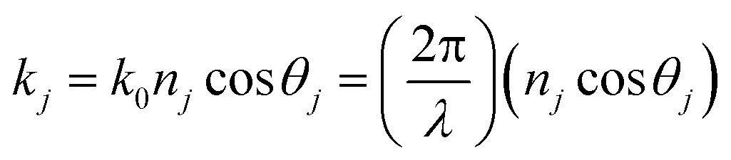 to define the wave vector component along the Z direction as a function of the incident angle (θj), the refractive index (nj) and the wavelength of the incident radiation (λ), then, Uj and Vj as the amplitudes of the fields components. Now eqn (1b) can be written in a more generalized form in the vicinity of eqn (1a) as: