DOI:
10.1039/D2RA04038G
(Paper)
RSC Adv., 2022,
12, 24146-24155
Physical insights into the Au growth on the surface of a LaAlO3/SrTiO3 heterointerface†
Received
30th June 2022
, Accepted 10th August 2022
First published on 25th August 2022
Abstract
Researchers investigated the modification of the LaAlO3/SrTiO3 interface with Au overlayers and nanoparticles, which led to the change of various physical properties. However, no research is available to elucidate insights into the interaction of Au with the LaAlO3/SrTiO3 substrate. Therefore, this study is devoted to solving the question using density functional theory calculations. We also studied the optical properties of the LaAlO3/SrTiO3 system before and after the Au adsorption. We found that an additional optical peak occurs with significant intensity in the wavelength region of 600 nm to 1200 nm depending on the LaAlO3 film thickness. This peak is attributed to the increase in the hole states in the presence of Au adsorption with the increase in the LaAlO3 film thickness.
1. Introduction
Making a heterointerface of oxide materials is a method that allows for the exploration of new physical phenomena leading to breakthrough technological applications that have never been found for bulk systems. The symmetry breaking of the crystal structure, charge, spin, and electronic orbitals at the interface of oxide materials are the cause for the creation of new electronic and optical properties such as two-dimensional electron gas (2DEG), which has been found in the heterointerface of oxide materials.1
Oxide heterointerfaces of common interest are perovskite systems.2–6 LaAlO3/SrTiO3 (abbreviated as LAO/STO) is the most attractive system due to the first discovery of a two-dimensional electron gas in 2004 (ref. 7) and crucial properties such as controllable two-dimensional electron conduction, Rashba spin–orbit interactions, superconducting property, and particularly a high electron mobility of ∼10![[thin space (1/6-em)]](https://www.rsc.org/images/entities/char_2009.gif) 000 cm2 V−1 s−1 at room temperature.8 Both LAO and STO perovskite crystals were known as wide band gap dielectrics (5.5 eV for LAO and 3.1 eV for STO), and the coupling of the LAO film layers on the STO substrate led to a transition from dielectric to metal. The transition occurred at the LAO film thickness of 4 unit cells.9 Due to their ionic nature, the STO polarization substrate and the LAO nonpolar film formed an interface with high polarity. This property establishes an electrostatic potential, which increases as the LAO thickness increases, leading to the restructuring of electronic properties with the charge transfer from LAO to STO.10 Several factors can affect the electronic conducting properties of the LAO/STO system: (1) oxygen vacancies, created during the fabrication process,11 generate donor levels located near the conduction band of STO,12 thereby changing the 2DEG state in the interface. (2) Pressure affects the existence and stability of two-dimensional electron gas.13 The compression pressure induces ferroelectric polarization in the STO substrate, thereby altering the 2-dimensional electron gas by reversing the polarization direction of the STO substrate due to charge passivation and band gap alignment. Experiments also showed that the STO stretching destroys the 2DEG state, while the STO compressive pressure maintains the 2DEG state, but the carrier density decreases compared to the LAO/STO system without pressure.14 (3) The electromagnetic properties of LAO/STO are affected by the carrier density of the system. The oxygen pressure conditions of the LAO layer growing modified the carrier density, where the O vacancies acted as electron donors. Besides, the coating of metal layers15,16 and other compounds on the LAO/STO surface17 also altered the carrier concentration. Electrons migrate from the coating material to the heterointerface via the LAO film and modify the carrier concentration and the electrical and thermal conductivity of the LAO/STO heterointerface. Therefore, the molecular adsorption, metal coating,18–20 and dispersion of metal nanoparticles21 on the LAO/STO surface have become effective methods to tune the 2DEG states. Metal coating and nanoparticle dispersion produced the most significant effects.18–24
000 cm2 V−1 s−1 at room temperature.8 Both LAO and STO perovskite crystals were known as wide band gap dielectrics (5.5 eV for LAO and 3.1 eV for STO), and the coupling of the LAO film layers on the STO substrate led to a transition from dielectric to metal. The transition occurred at the LAO film thickness of 4 unit cells.9 Due to their ionic nature, the STO polarization substrate and the LAO nonpolar film formed an interface with high polarity. This property establishes an electrostatic potential, which increases as the LAO thickness increases, leading to the restructuring of electronic properties with the charge transfer from LAO to STO.10 Several factors can affect the electronic conducting properties of the LAO/STO system: (1) oxygen vacancies, created during the fabrication process,11 generate donor levels located near the conduction band of STO,12 thereby changing the 2DEG state in the interface. (2) Pressure affects the existence and stability of two-dimensional electron gas.13 The compression pressure induces ferroelectric polarization in the STO substrate, thereby altering the 2-dimensional electron gas by reversing the polarization direction of the STO substrate due to charge passivation and band gap alignment. Experiments also showed that the STO stretching destroys the 2DEG state, while the STO compressive pressure maintains the 2DEG state, but the carrier density decreases compared to the LAO/STO system without pressure.14 (3) The electromagnetic properties of LAO/STO are affected by the carrier density of the system. The oxygen pressure conditions of the LAO layer growing modified the carrier density, where the O vacancies acted as electron donors. Besides, the coating of metal layers15,16 and other compounds on the LAO/STO surface17 also altered the carrier concentration. Electrons migrate from the coating material to the heterointerface via the LAO film and modify the carrier concentration and the electrical and thermal conductivity of the LAO/STO heterointerface. Therefore, the molecular adsorption, metal coating,18–20 and dispersion of metal nanoparticles21 on the LAO/STO surface have become effective methods to tune the 2DEG states. Metal coating and nanoparticle dispersion produced the most significant effects.18–24
The Au coating on the LAO/STO system has been fabricated.16,22 However, no research is available to elucidate the effects of Au adsorption on the electronic and optical properties of the LAO/STO heterointerface. Therefore, we decided to research in order to clarify the topic by employing density functional theory calculations.
2. Structure model and computational method
To understand the influences of the Au adsorption on the electronic and optical properties of LAO/STO, we studied the band structure, the electronic density of states, and the dielectric function of LAO/STO before and after the Au adsorption. We used the density functional theory calculations via the Vienna ab initio simulation package.25 We treated the core-valence interaction and the exchange-correlation functional in the projector-augmented wave method26,27 and the Perdew–Burke–Ernzerhof generalized gradient approximation,28,29 respectively. We performed the plane wave expansion at the kinetic energy cut-off of 650 eV. The Brillouin zone integration used the special-point sampling technique of Monkhorst and Pack30 with a k-point mesh sample of 13 × 13 × 1. The simulation for the periodic supercell included dipole corrections.31,32 We improved the convergence speed of the calculations by the Gaussian-smearing method33 with the sigma value of 0.1 eV. All atomic positions were allowed to fully relax during the geometry optimization until the Hellmann–Feynman force acting on each atom reached 10−3 eV Å−1. The non-spin-polarized scheme was performed for the geometry optimization, electronic band structure, and the density of states. We also tested the spin-polarized option for the isolated Au atom. However, the total energy of the isolated Au atom was almost the same as that of the non-spin-polarized calculation.
The LAO/STO system was modelled by (LAO)m/(STO)4 superlattices with m = 1–6 layers, which were constructed using a slab of 2 × 2 unit cell and a vacuum space of approximately 35.0 Å along the surface normal, see Fig. 1.
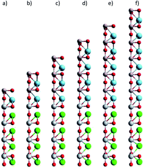 |
| | Fig. 1 The slab model of (LAO)m/STO4 substrate: (a)–(f) for m = 1–6 layers, respectively. Brown (Al), red (O), cyan (La), grey (Ti), green (Sr). | |
The adsorption energy of an Au atom was determined by
| | |
Ea = EAu@LAO/STO − (ELAO/STO + EAu).
| (1) |
where
EAu@LAO/STO,
ELAO/STO, and
EAu are the total energies of the Au@LAO/STO system, the clean LAO/STO slab, and the isolated Au atom, respectively. The adsorption of Au atom on the LAO/STO slab corresponds to the Au density of 6.5 × 10
14 cm
−2.
22
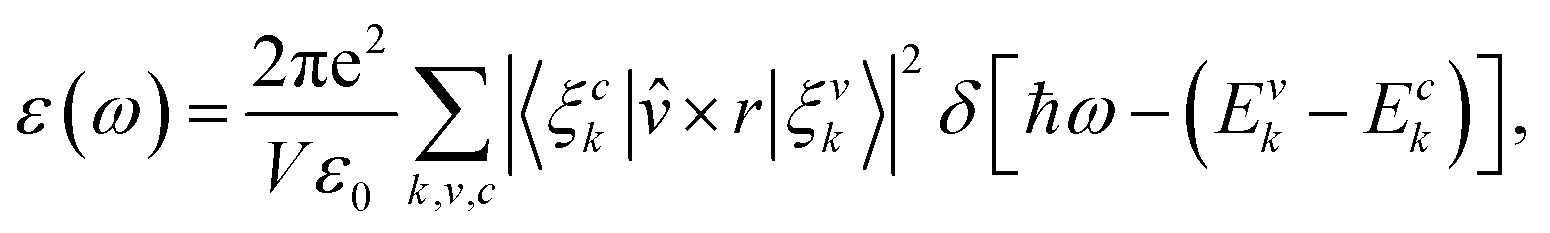
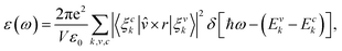
To describe the optical properties of the LAO/STO and Au@LAO/STO systems, we calculated the imaginary part of the frequency-dependent dielectric function of the form:34–36
| |
 | (2) |
where
ω and
ε0 are the frequency of emission and the dielectric constant of free space, respectively.
ξvk (
ξck) is the valence (conduction) band wave function.
V and
![[v with combining circumflex]](https://www.rsc.org/images/entities/i_char_0076_0302.gif)
are the unit cell volume and the polarization vector of the electric field of the emission, respectively.
3. Results and discussion
3.1. Au adsorption on LAO/STO
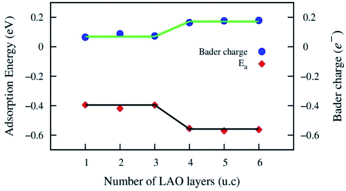
The Au atom initially was placed on possible adsorption sites of the LAO topmost layer, i.e., top sites (on the O, Al, and La atoms), bridge sites (on Al–O and La–O), and the hollow site of the 2 × 2 unit cell (see Fig. 2). On each adsorption site, after performing the geometry optimization, we obtained the adsorption energy of the Au atom on the LAO/STO interface. We found that the most favourable adsorption site of the Au atom is located on the Al–O bridge. Table 1 lists the adsorption energy and the bond distances from the Au atom on the Al–O bridge to the nearest atom in the LAO film. The average bond distance from the Au atom to the O and Al atoms of the LAO topmost layer is about 2.57 Å. The adsorption energy is more significant for the LAO film thickness of 4, 5, and 6 unit cells than those of 1, 2, and 3 unit cells. Fig. 3 shows that the adsorption energy exhibits the down-stair behaviour at the LAO film thickness of 4 unit cells, where the adsorption energy suddenly becomes more negative by approximately 0.15 eV. We also calculated the adsorption energy of the Au atom on the 4 × 4 unit cell of the LAO/STO substrates to understand the tendency of the Au coverage modification. We found that the adsorption energy of the Au atom on the 4 × 4 unit cell becomes more negative than that of the 2 × 2 unit cell by about 0.3 eV. Therefore, we predict that increasing the Au coverage on the LAO/STO system decreases the adsorption energy per Au atom.
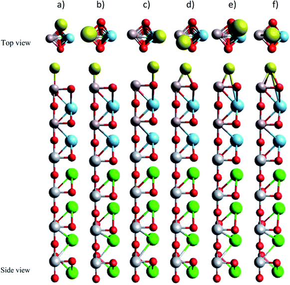 |
| | Fig. 2 The adsorption sites for the Au atom on the (LAO)2/(STO)4 slab: (a) to (f) present the top site of the O, Al, and La atoms, the bridge site of Al–O and La–O, and the hollow site, respectively. Top view (upper panel) and side view (lower panel). Yellow (Au), brown (Al), red (O), cyan (La), grey (Ti), green (Sr). | |
Table 1 Adsorption energy of the Au atom and bond distances from the Au atom to the nearest atoms of the LAO topmost layer at the most favourable adsorption site, i.e., the Al–O bridge site
| LAO film thickness in unit cell (u.c.) |
Bond distances (Å) |
Adsorption energy (eV) |
| 1 |
2.64 (O), 2.57 (Al) |
−0.3947 |
| 2 |
2.62 (O), 2.56 (Al) |
−0.4187 |
| 3 |
2.64 (O), 2.61 (Al) |
−0.3960 |
| 4 |
2.51 (O), 2.56 (Al) |
−0.5547 |
| 5 |
2.55 (O), 2.59 (Al) |
−0.5710 |
| 6 |
2.45 (O), 2.56 (Al) |
−0.5627 |
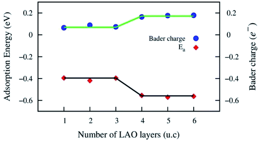 |
| | Fig. 3 The Au adsorption energy and the Bader charge exchange versus the LAO film thickness from 1 to 6 unit cells. The solid lines describe the trend of the physical parameters. | |
3.2. Electronic properties
To clarify how the Au adsorption changes the electronic properties of the LAO/STO interface, we first analyse the Bader point charge exchange between the LAO film and the STO substrate before and after the Au adsorption. The calculation of the Bader point charge exchange proceeds via two steps: (1) calculation of the point charge of the atoms in the system using the Bader partition technique.37–40 (2) Subtraction of the neutral charge of the corresponding isolated atoms from the point charge obtained in step (1). Table 2 shows that, before the Au adsorption, the LAO film always transfers a fraction of the negative charge (e−) to the STO substrate. This charge exchange has a more significant value for the LAO unit thickness of ≥4 unit cells than of ≤3 unit cells. Fig. 3 shows a correlation between the behaviour of the Bader charge exchange in the LAO/STO system and the Au adsorption energy. The charge exchange increases, while the adsorption energy becomes more negative as the LAO film thickness approaches 4 unit cells. At this point, we can express that the nature of the interaction between the Au atom and the LAO/STO interface is due to the charge exchange; however, to gain insights into the interaction, we have to analyse further the electronic band structure and electronic density of states. The charge loss of the LAO film is more profound in the presence of the Au atom because the Au atom gains charge, while the charge gain of the STO substrate slightly increases compared to that of the clean LAO/STO system. The charge accumulation in the Au atom somehow decreases as the LAO film thickness increases, which is opposite to the trend of the charge gain of the STO substrate. The layer-resolved charge for the Au@LAO/STO system in Table 3 shows that the charge loss of the LAO film mainly occurs at the LAO layer that interfaces with the STO substrate, while the charge gain of the STO substrate mainly focuses on the STO bottom layer.
Table 2 Bader charge (e−) of the LAO film, the STO substrate, and the Au atom adsorbed on the LAO/STO slab: (+) charge gain, (−) charge loss
| LAO film thickness in unit cell (u.c.) |
1 |
2 |
3 |
4 |
5 |
6 |
| LAO/STO |
LAO |
−0.065 |
−0.088 |
−0.073 |
−0.164 |
−0.176 |
−0.179 |
| STO |
+0.065 |
+0.088 |
+0.073 |
+0.164 |
+0.176 |
+0.179 |
| Au@LAO/STO |
LAO |
−0.275 |
−0.274 |
−0.251 |
−0.299 |
−0.312 |
−0.311 |
| STO |
+0.069 |
+0.090 |
+0.086 |
+0.172 |
+0.179 |
+0.183 |
| Au |
+0.206 |
+0.183 |
+0.165 |
+0.127 |
+0.133 |
+0.128 |
Table 3 The layer resolved Bader charge (e−) for the LAO/STO and Au@LAO/STO systems: (+) charge gain, (−) charge loss
| LAO film thickness in unit cell (u.c.) |
1 |
2 |
3 |
4 |
5 |
6 |
| The interface layers of LAO and STO were denoted as LAO1 and STO1, respectively. |
| LAO/STO |
LAO6 |
|
|
|
|
|
+0.024 |
| LAO5 |
|
|
|
|
+0.016 |
+0.014 |
| LAO4 |
|
|
|
−0.042 |
+0.014 |
−0.004 |
| LAO3 |
|
|
+0.113 |
−0.013 |
+0.014 |
+0.001 |
| LAO2 |
|
+0.135 |
+0.034 |
−0.013 |
−0.003 |
+0.014 |
| LAO1a |
−0.065 |
−0.223 |
−0.220 |
−0.181 |
−0.218 |
−0.227 |
| STO1a |
−0.020 |
−0.006 |
−0.033 |
−0.013 |
+0.005 |
+0.033 |
| STO2 |
−0.005 |
+0.003 |
+0.004 |
+0.017 |
+0.017 |
+0.005 |
| STO3 |
−0.009 |
−0.008 |
−0.004 |
+0.014 |
+0.031 |
+0.038 |
| STO4 |
+0.099 |
+0.098 |
+0.106 |
+0.146 |
+0.124 |
+0.103 |
| Au@LAO/STO |
LAO6 |
|
|
|
|
|
−0.115 |
| LAO5 |
|
|
|
|
−0.104 |
+0.016 |
| LAO4 |
|
|
|
−0.132 |
+0.002 |
−0.004 |
| LAO3 |
|
|
−0.083 |
+0.014 |
+0.036 |
+0.003 |
| LAO2 |
|
−0.052 |
+0.029 |
−0.015 |
−0.014 |
+0.012 |
| LAO1a |
−0.275 |
−0.221 |
−0.197 |
−0.167 |
−0.231 |
−0.222 |
| STO1a |
−0.019 |
−0.004 |
−0.031 |
−0.008 |
+0.028 |
+0.034 |
| STO2 |
−0.004 |
+0.003 |
+0.009 |
+0.021 |
+0.017 |
+0.009 |
| STO3 |
−0.008 |
−0.010 |
−0.004 |
+0.015 |
+0.009 |
+0.037 |
| STO4 |
+0.100 |
+0.101 |
+0.112 |
+0.145 |
+0.125 |
+0.102 |
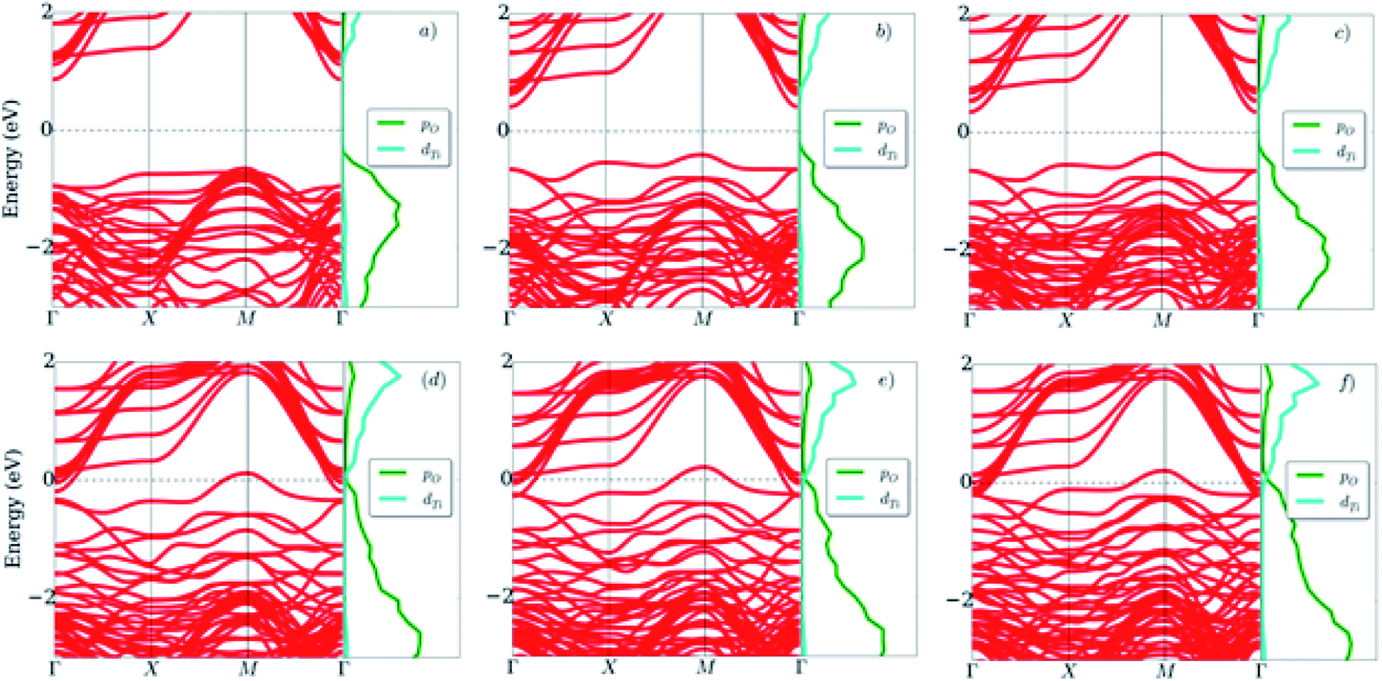
Fig. 4 shows that, for the LAO/STO interface, the bottom of the conduction band and the top of the valence band are mainly attributed to the Ti 3d orbital of the STO substrate and the O 2p orbital of the LAO film, respectively. When the LAO film thickness increases, the conduction band shifts downward, while the valence band shifts upward. These shifts narrow the energy band gap, i.e., the energy difference between the conduction band minimum and the valence band maximum. Fig. 5 displays the dependence of the band gap on the LAO film thickness. We find that the LAO/STO heterointerface has an indirect band gap at the Γ and M points in the Brillouin zone (Fig. 4) and hence exhibits an insulating behaviour for the LAO film thickness of 1 to 3 unit cells (Fig. 5). However, for the LAO film thickness of ≥4 unit cells, the LAO/STO heterointerface shows a metallic behaviour because the Ti 3d orbital state of the conduction band and the O 2p orbital state of the valence band cross over the Fermi level forming the 2DEG states in the valence band and the hole states in the conduction band, respectively. The decreasing trend of the band gap with the increase in the LAO film thickness correlates well with the sudden increase of the Bader charge exchange between the LAO film and the STO substrate and hence the Au adsorption energy, see Table 2 and Fig. 3. The transformation of the nature of the LAO/STO heterointerface from insulating to metallic for the critical LAO film thickness of 4 unit cells is in good agreement with the significant charge exchange of the LAO and STO layers and also the previous publications.7,9 Therefore, we can emphasize that the binding of the Au atom with the LAO/STO interface correlates very well with the transition from semiconductor to metal nature of the interface. We also have to emphasize that the transition from semiconductor to metal at the LAO film thickness of 4 u.c. of the clean LAO/STO system is independent of the particular setting of the STO substrate thickness of 4 layers. In the ESI,† Fig. S shows that the transition also occurs at the same LAO thickness of 4 unit cells for STO layers of 6 unit cells.
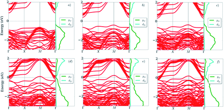 |
| | Fig. 4 The band structure and the density of states (DOS) of the LAO/STO interface: (a)–(f) corresponding to the heterointerface with the LAO film thickness of 1 to 6 unit cells. The top of the valence band belongs to the LAO unit cell interface with the STO substrate. The Fermi level is at 0 eV. | |
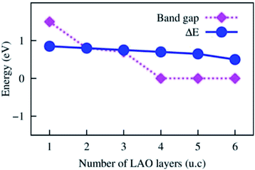 |
| | Fig. 5 The energy bandgap of the LAO/STO slab and the energy difference (ΔE) between the lowest energy level of the Au 6s band at the Γ point and the Fermi level of the Au@LAO/STO system versus the LAO film thickness. | |
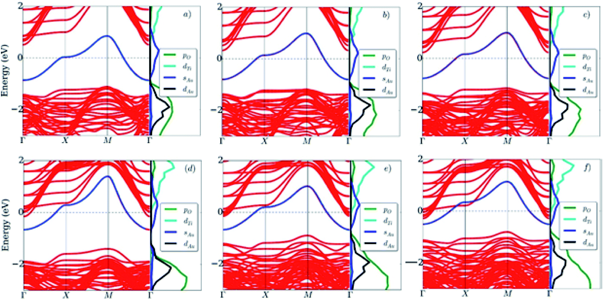
For the Au@LAO/STO system, Fig. 6 shows that the top of the valence band is located at lower energy levels compared to that of the clean LAO/STO slab owing to a significant charge loss of the LAO film that reduces the electron occupancy in the valence band. Simultaneously, the Ti 3d state of the STO substrate remains on the trend of a downward shift because the charge gain of the STO substrate slightly increases compared to that of the clean LAO/STO system. The Au 5d orbital contributes to the top of the valence band, while the Au 6s orbital mainly distributes around the Fermi level. Therefore, a new energy band appears in the band gap region between the conduction and valence bands of the Au@LAO/STO substrate. The new band trapping in the band gap region is responsible for the formation of the new 2DEG states and the hole states below and above the Fermi level, respectively. The new 2DEG states enhance the electronic occupation around the Fermi level, and hence, improve the conductivity of the Au@LAO/STO system compared to the LAO/STO system as observed by the experiment.22 We also find that the LAO film thickness increases as the new energy band (the Au 6s orbital) moves upward to the conduction band of the LAO/STO substrate, thereby reducing the 2DEG states and simultaneously enhancing the hole states of the Au@LAO/STO system. Quantitatively, we described the relative position of the Au 6s band to the Fermi level by calculating the energy difference ΔE between the Fermi level and the bottom energy level of the Au 6s band at the Γ point. Fig. 5 shows that ΔE decreases monotonically, which implies that the hole states increase while the 2DEG states decrease with the LAO film thickness. The reduction of the 2DEG occupation state was found to be consistent with the trend of the Au charge gain as seen in Table 2.
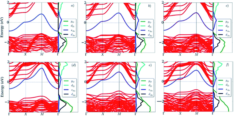 |
| | Fig. 6 The band structure and the density of states (DOS) of the Au@LAO/STO system: (a)–(f) correspond to the heterointerface with the LAO film thickness of 1 to 6 unit cells. The Fermi level is at 0 eV. | |
We presented the orbital-projected density of states of the LAO/STO and Au@LAO/STO systems for the most meaningful orbitals around the Fermi level in Fig. 7. This figure shows that the valence band maximum and the conduction band minimum of the LAO/STO heterointerface crossing the Fermi level as the LAO film thickness increases is due to the upshift of the O px, py, and pz orbitals of the LAO film (Fig. 7a) and the downshift of the Ti dxy, dxz, and dyz orbitals of the STO layers (Fig. 7b). After the Au adsorption, the O pz state of the LAO film is broadened over the Fermi level (Fig. 7c) to establish the interaction with the s and dz2 states of the Au atom (Fig. 7f). Besides, the Au dz2 state also slightly increases across the Fermi level as the LAO layers increases. The changes in the presence of the Au atom generated the new 2DEG and hole states of the LAO/STO system. For the STO substrate in Fig. 7d, we can see that the downshift of the Ti dxy, dxz, and dyz orbitals also occurs, which is similar to that of the clean LAO/STO system but with a faster speed across the Fermi level.
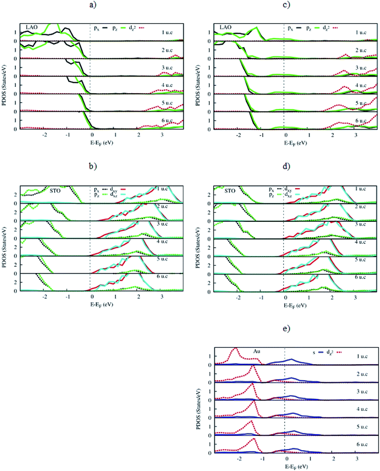 |
| | Fig. 7 The orbital-projected density of states (PDOS) of the LAO/STO (left panel) and the Au@LAO/STO (right panel) systems. In figures (a), (b), (c), and (d,) the px and py orbitals are identical. In figures (b) and (d), dxz, and dyz are identical. The Fermi level is at 0 eV. | |
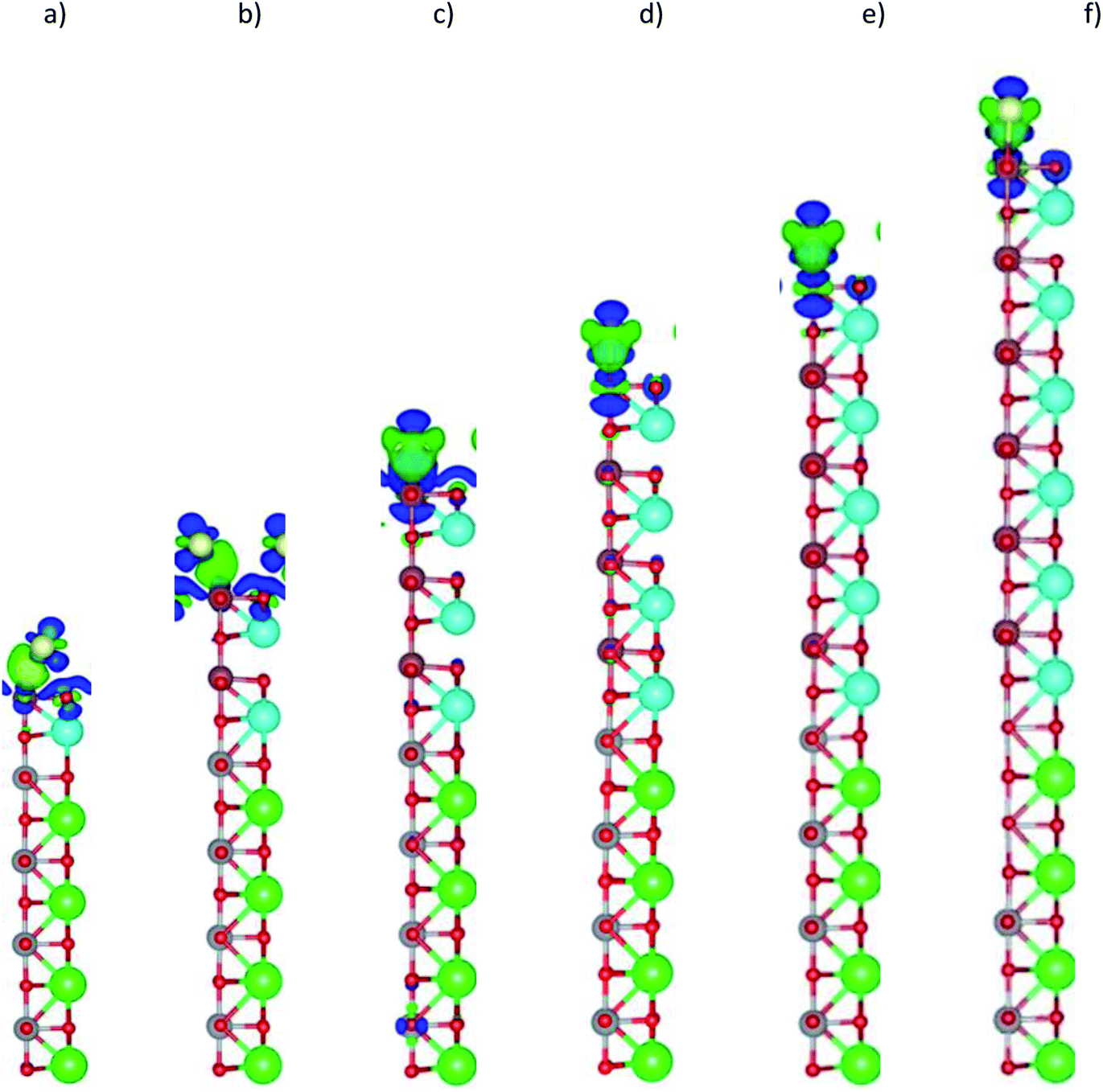
The charge clouds of the Au atom and the O atoms in the topmost layer show the shape of the Au s, Au dz2, and O pz orbitals (Fig. 8). The charge donation and accumulation are distributed on the topmost layer of the LAO film and the Au atom, respectively. This result is in good agreement with the orbital-projected DOS in Fig. 7.
 |
| | Fig. 8 The charge density difference of the Au@(LAO)m/STO4 system, (a)–(f) for the LAO film thickness of 1 to 6 unit cells. Occupied and unoccupied states are presented in green and blue, respectively. | |
3.3. Optical properties
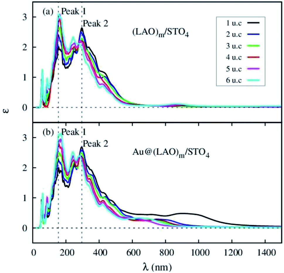
We studied the optical properties of the LAO/STO and Au@LAO/STO systems via the imaginary part ε(ω) of the frequency-dependent dielectric function in the independent particle approximation. The imaginary part is an important parameter of the dielectric function that evaluates the ability of a material to absorb and emit light. The photon energy Ep corresponding to the peaks of the imaginary dielectric function was also determined in the calculation. The photon wavelength was obtained from the photon energy through the following formula λ = hc/Ep, where h is the Planck constant and c is the speed of light in vacuum. The imaginary dielectric function of the LAO/STO system before and after Au adsorption is plotted in Fig. 9 and the values are listed in Table 4.
 |
| | Fig. 9 The imaginary dielectric function ε versus wavelength λ for (a) (LAO)m/STO4 and (b) Au@(LAO)m/STO4 systems (m = 1, 2, 3, 4, 5, 6 u.c.). | |
Table 4 The wavelength and dielectric function at the main and additional optical peaks
| |
LAO film thickness |
| 1 u.c. |
2 u.c. |
3 u.c. |
4 u.c. |
5 u.c. |
6 u.c. |
| The photon wavelength λ = hc/Ep, where, Ep is the photon energy, h is Planck constant, and c is the speed of light in vacuum. |
| Peak 1 |
| LAO/STO |
Ep1 (eV) |
7.97 |
7.96 |
7.97 |
7.98 |
7.59 |
7.98 |
| λ1 (nm)a |
155.51 |
155.64 |
155.41 |
155.41 |
163.39 |
155.30 |
| ε1 |
2.02 |
2.39 |
2.67 |
2.85 |
3.09 |
3.10 |
| Au@LAO/STO |
Ep1 (eV) |
7.43 |
7.29 |
8.03 |
7.85 |
7.33 |
7.67 |
| λ1 (nm)a |
166.88 |
170.02 |
154.43 |
157.94 |
169.14 |
161.73 |
| ε1 |
1.91 |
2.17 |
2.51 |
2.79 |
2.95 |
3.09 |
|
| Peak 2 |
| LAO/STO |
Ep2 (eV) |
4.19 |
4.26 |
4.21 |
4.22 |
4.34 |
4.43 |
| λ2 (nm)a |
296.01 |
290.90 |
294.74 |
293.76 |
285.65 |
279.97 |
| ε2 |
2.64 |
2.49 |
2.30 |
2.22 |
2.21 |
2.12 |
| Au@LAO/STO |
Ep2 (eV) |
4.19 |
4.26 |
4.22 |
4.29 |
5.10 |
4.38 |
| λ2 (nm)a |
295.88 |
291.29 |
293.85 |
290.48 |
283.20 |
283.03 |
| ε2 |
2.68 |
2.59 |
2.50 |
2.39 |
2.39 |
2.38 |
|
| Additional peak |
| LAO/STO |
Ep3 (eV) |
|
|
|
1.37 |
1.40 |
1.43 |
| λ3 (nm)a |
|
|
|
905.76 |
887.98 |
864.27 |
| ε3 |
|
|
|
0.06 |
0.10 |
0.12 |
| Au@LAO/STO |
Ep3 (eV) |
1.37 |
1.64 |
1.76 |
1.73 |
2.93 |
1.95 |
| λ3 (nm)a |
906.95 |
757.36 |
705.23 |
716.19 |
642.22 |
636.81 |
| ε3 |
0.48 |
0.29 |
0.27 |
0.27 |
0.299 |
0.33 |
We observe that the imaginary dielectric function of the clean LAO/STO interface shows the spectrum in the wavelength region from 100 nm to 1000 nm. The system exhibits two majority optical peaks at 155 nm and 290 nm in the ultraviolet region and one minority peak in the range of 800–1000 nm. As the number of the LAO layers increases, the intensity of Peak 1 enhances but that of Peak 2 decreases. Noticeably, the minority peak occurs only for the LAO film thickness of 4, 5, and 6 unit cells. The imaginary dielectric function of the Au@LAO/STO system also has the same character as that of the clean LAO/STO system with little difference, i.e., the additional peak occurs in the range from 600 to 1200 nm regardless of the LAO film thickness. When the LAO thickness increases, the peak shifts to a shorter wavelength and simultaneously decreases the intensity. Also, the height of the additional peak for the Au@LAO/STO system is significantly higher than that for the clean LAO/STO system. We found that the minority peaks in the dielectric function of the clean LAO/STO and Au@LAO/STO systems are consistent with the existence of the hole states in the electronic band structures, as shown in Fig. 4 and 6.
4. Conclusions
Two main optical peaks of the clean LAO/STO and Au@LAO/STO systems occur around 160 and 290 nm, respectively. Besides, there is a minority peak around 900 nm for the clean LAO/STO system for the LAO film thickness of ≥4 unit cells and in the range of 700–1200 nm for the Au@LAO/STO system regardless of the LAO film thickness. The additional optical peak emerges because of the existence of hole states, which are associated with the transition from semiconductor to metal of the clean LAO/STO substrate at the critical LAO film thickness of 4 unit cells, and the significant enhancement of the hole states in the presence of the Au adsorption. The charge exchange between Au and LAO explained the interaction of the Au atom and the LAO/STO substrate. Finally, the O pz orbitals of the LAO film and the Au 6s and dz2 orbitals dominated the interaction. It is well-known that the GGA-PBE approximation often underestimates the energy band gap and therefore influences the accuracy of the optical properties. The HSE functional and GW approximation can improve the accuracy of the energy band gap calculations. The current work only performed the GGA-PBE approximation. However, we could capture the tendency of the optical peak modifications after the change of the LAO film thickness and the physics of the Au adsorption.
Conflicts of interest
There are no conflicts of interest to declare.
Acknowledgements
We acknowledge Ho Chi Minh City University of Technology (HCMUT), VNU-HCM for supporting this study.
References
- J. Mannhart, D. H. A. Blank, H. Y. Hwang, A. J. Millis and J.-M. Triscone, Two-dimensional electron gas at oxides interfaces, MRS Bull., 2008, 33(11), 1027–1034 CrossRef CAS.
- V. Maznichenko, S. Ostanin, A. Ernst, J. Henk and I. Mertig, Formation and Tuning of 2D Electron Gas in Perovskite Heterostructures, Phys. Rev. B, 2020, 257, 1900540 Search PubMed.
- P. Subko, S. Gariglio, M. Gabay, P. Ghosez and J. M. Triscone, Interface Physics in Complex Oxide Heterostructures, Annu. Rev. Condens. Matter Phys., 2011, 2, 141 CrossRef.
- M. Grundmann, R. Karsthof and H. von Wenckstern, Interface Recombination Current in Type II Heterostructure Bipolar Diodes, ACS Appl. Mater. Interfaces, 2014, 6, 14785 CrossRef CAS PubMed.
- C. Yang, M. Kneib, F. L. Schein, M. Lorenz and M. Grundmann, Room-temperature Domain-epitaxy of Copper Iodide Thin Films for Transparent CuI/ZnO Heterojunctions with High Rectification Ratios Larger than 109, Sci. Rep., 2016, 6, 21937 CrossRef CAS PubMed.
- W. Harrison, E. Kraut, J. Waldrop and R. Grant, Polar heterojunction interfaces, Phys. Rev. B: Solid State, 1978, 18, 4402 CrossRef CAS.
- A. Ohtomo and H. Y. Hwang, A high-mobility electron gas at the LaAlO3/SrTiO3 heterointerface, Nature, 2004, 427, 423 CrossRef CAS PubMed.
- K. Han, K. Hu, X. Li, K. Huang, Z. Huang, S. Zeng, D. Qi, C. Ye, J. Yang and X. R. Wang, Erasable and recreatable two-dimensional electron gas at the heterointerface of SrTiO3 and a water-dissolvable overlaye, Sci. Adv., 2019, 5, eaaw7286 CrossRef CAS PubMed.
- S. Thiel, G. Hammerl, A. Schmehl, C. W. Schneider and J. Mannhart, Tunable quasi-two-dimensional electron gases in oxide heterostructures, Science, 2006, 313, 1942 CrossRef CAS PubMed.
- N. Nakagawa, H. Y. Hwang and D. A. Muller, Why some interfaces cannot be sharp, Nat. Mater., 2006, 5, 204 CrossRef CAS.
- J. N. Eckstein, Watch Out for the Lack of Oxygen, Nat. Mater., 2007, 6, 473 CrossRef CAS PubMed.
- Z. Q. Liu, D. P. Leusink, X. Wang, W. M. Lu, K. Gopinadhan, A. Annadi, Y. L. Zhao, X. H. Huang, A. Srivastava, S. Dhar and T. Venkatesan, Ariando, Metal-Insulator Transition in SrTiO3−x Thin Films Induced by Frozen-Out Carriers, Phys. Rev. Lett., 2011, 107, 146802 CrossRef CAS PubMed.
- H. Guo, W. A. Saidi and J. Zhao, Tunability of the two-dimensional electron gas at the LaAlO3/SrTiO3 interface by strain-induced ferroelectricity, Phys. Chem. Chem. Phys., 2016, 18, 28474 RSC.
- C. W. Bark, D. A. Felker, Y. Wang, Y. Zhang, H. W. Jang, C. M. Folkman, J. W. Park, S. H. Baek, H. Zhou, D. D. Fong, X. Q. Pan, E. Y. Tsymbal, M. S. Rzchowski and C. B. Eom, Tailoring a two-dimensional electron gas at the LaAlO3/SrTiO3 (001) interface by epitaxial strain, Proc. Natl. Acad. Sci. U. S. A., 2011, 108, 4720 CrossRef CAS.
- B. Forg, C. Richter and J. Mannhart, Field-effect devices utilizing LaAlO3-SrTiO3 interfaces, Appl. Phys. Lett., 2012, 100, 053506 CrossRef.
- Y. Zhou, Y. J. Shi, S. W. Jiang, F. J. Yue, P. Wang, H. F. Ding and D. Wu, Tuning carrier density at complex oxide interface with metallic overlayer, Appl. Phys. Lett., 2016, 108, 231603 CrossRef.
- V. T. Tra, J.-W. Chen and P.-C. Huang, Ferroelectric Control of the Conduction at the LaAlO3/SrTiO3 Heterointerface, Adv. Mater., 2013, 25, 3357 CrossRef CAS PubMed.
- K. Au, D. F. Li, N. Y. Chan and J. Y. Dai, Polar liquid molecule induced transport property modulation at LaAlO3/SrTiO3 heterointerface, Adv. Mater., 2012, 24, 2598 CrossRef CAS PubMed.
- Y. F. Dong, Y. Y. Mi, Y. P. Feng, A. C. H. Huan and S. J. Wang, Ab initio studies on Schottky barrier heights at metal gate/LaAlO3 (001) interfaces, Appl. Phys. Lett., 2006, 89, 122115 CrossRef.
- R. Arras, V. G. Ruiz, W. E. Pickett and R. Pentcheva, Tuning the two-dimensional electron gas at the LaAlO3/SrTiO3(001) interface by metallic contacts, Phys. Rev. B: Condens. Matter Mater. Phys., 2012, 85, 125404 CrossRef.
- H. Kim, N. Y. Chan, J. Dai and D.-W. Kim, Enhanced Surface-and-Interface Coupling in Pd-Nanoparticle-coated LaAlO3/SrTiO3 Heterostructures: Strong Gas- and Photo-Induced Conductance Modulation, Sci. Rep., 2015, 5, 8531 CrossRef CAS PubMed.
- D. C. Vaz, E. Lesne, A. Sander, H. Naganuma, E. Jacquet, J. Santamaria, A. Barthélémy and M. Bibes, Tuning Up or Down the Critical Thickness in LaAlO3/SrTiO3 through in Situ Deposition of Metal Overlayers, Adv. Mater., 2017, 29, 1700486 CrossRef PubMed.
- R. Pentcheva, R. Arras, K. Otte, V. G. Ruiz and W. E. Pickkett, Termination control of electronic phases in oxide thin films and interfaces: LaAlO3/SrTiO3(001), Philos. Trans. R. Soc., A, 2012, 370, 4904 CrossRef CAS PubMed.
- E. Lesne, N. Reyren, D. Doennig, R. Mattana, H. Jaffrès, V. Cros, F. Petroff, F. Choueikani, P. Ohresser, R. Pentcheva, A. Barthélémy and M. Bibes, Suppression of the critical thickness threshold for conductivity at the LaAlO3/SrTiO3 interface, Nat. Commun., 2014, 5, 4291 CrossRef CAS PubMed.
- G. Kresse and J. Furthmuller, Efficient iterative schemes for ab initio total-energy calculations using a plane-wave basis set, Phys. Rev. B: Condens. Matter Mater. Phys., 1996, 54, 11169 CrossRef CAS PubMed.
- P. E. Blochl, Projector augmented-wave method, Phys. Rev. B: Condens. Matter Mater. Phys., 1994, 50, 17953 CrossRef PubMed.
- G. Kresse and J. Joubert, From ultrasoft pseudopotentials to the projector augmented-wave method, Phys. Rev. B: Condens. Matter Mater. Phys., 1999, 59, 1758 CrossRef CAS.
- J. P. Perdew, J. A. Chevary, S. H. Vosko, K. A. Jackson, M. R. Pederson, D. J. Singh and C. Fiolhais, Atoms, molecules, solids, and surfaces: Applications of the generalized gradient approximation for exchange and correlation, Phys. Rev. B: Condens. Matter Mater. Phys., 1992, 46, 6671 CrossRef CAS PubMed.
- J. P. Perdew, K. Burke and M. Ernzerhof, Generalized Gradient Approximation Made Simple, Phys. Rev. Lett., 1996, 77, 3865 CrossRef CAS PubMed.
- H. J. Monkhorst and J. D. Pack, Special points for Brillouin-zone integrations, Phys. Rev. B: Solid State, 1976, 13, 5188–5192 CrossRef.
- J. Neugebauer and M. Scheffler, Adsorbate-substrate and adsorbate-adsorbate interactions of Na and K adlayers on Al(111), Phys. Rev. B: Condens. Matter Mater. Phys., 1992, 46, 16067 CrossRef CAS PubMed.
- L. Bengtsson, Dipole correction for surface supercell calculations, Phys. Rev. B: Condens. Matter Mater. Phys., 1999, 59, 12301 CrossRef CAS.
- C. L. Fu and K. M. Ho, First-principles calculation of the equilibrium ground-state properties of transition metals: Applications to Nb and Mo, Phys. Rev. B: Condens. Matter Mater. Phys., 1983, 28, 5480 CrossRef CAS.
- S. Saha, T. P. Sinha and A. Mookerjee, Electronic structure, chemical bonding, and optical properties of paraelectric BaTiO3, Phys. Rev. B: Condens. Matter Mater. Phys., 2000, 62(13), 8828–8834 CrossRef CAS.
- L. J. Kong, G. H. Liu and L. Qiang, Electronic and optical properties of O-doped monolayer MoS2, Comput. Mater. Sci., 2016, 111, 416–423 CrossRef CAS.
- O. K. Le, V. Chihaia, M.-P. Pham-Ho and D. N. Son, Electronic and optical properties of monolayer MoS2 under the influence of polyethyleneimine adsorption and pressure, RSC Adv., 2020, 10, 4201–4210 RSC.
- G. Henkelman, A. Arnaldsson and H. Jónsson, A fast and robust algorithm for Bader decomposition of charge density, Comput. Mater. Sci., 2006, 36, 354–360 CrossRef.
- E. Sanville, S. D. Kenny, R. Smith and G. Henkelman, An improved grid-based algorithm for Bader charge allocation, J. Comput. Chem., 2007, 28, 899–908 CrossRef CAS PubMed.
- O. K. Le, V. Chihaia, V. Van On and D. N. Son, N-type and p-type molecular doping on monolayer MoS2, RSC Adv., 2021, 11(14), 8033–8041 RSC.
- V. K. Dien, O. K. Le, V. Chihaia, P.-H. My-Phuong and D. N. Son, Monolayer transition-metal dichalcogenides with polyethyleneimine adsorption, J. Comput. Electron., 2021, 20, 135–150 CrossRef CAS.
Footnote |
| † Electronic supplementary information (ESI) available: Physical insights into Au growth on surface of LaAlO3/SrTiO3 heterointerface. See https://doi.org/10.1039/d2ra04038g |
|
| This journal is © The Royal Society of Chemistry 2022 |
Click here to see how this site uses Cookies. View our privacy policy here. 
 Open Access Article
 This Open Access Article is licensed under a Creative Commons Attribution-Non Commercial 3.0 Unported Licence
 *ab
*ab