
 Open Access Article
 This Open Access Article is licensed under a Creative Commons Attribution-Non Commercial 3.0 Unported Licence
How varying surface wettability of different PEDOT:PSS formulations and their mixtures affects perovskite crystallization and the efficiency of inverted perovskite solar cells
Zekarias Teklu Gebremichael *abc,
Chikezie Ugokweab,
Shahidul Alamabd,
Steffi Stumpfae,
Marco Diegelf,
Ulrich S. Schubertabe and
Harald Hoppe*ab
*abc,
Chikezie Ugokweab,
Shahidul Alamabd,
Steffi Stumpfae,
Marco Diegelf,
Ulrich S. Schubertabe and
Harald Hoppe*ab
aLaboratory of Organic and Macromolecular Chemistry (IOMC), Friedrich Schiller University Jena, Humboldt Str. 10, 07743 Jena, Germany. E-mail: zekariasteklu.gebremichael@uni-jena.de; harald.hoppe@uni-jena.de
bCenter for Energy and Environmental Chemistry Jena (CEEC Jena), Friedrich Schiller University Jena, Philosophenweg 7a, 07743 Jena, Germany
cCollege of Natural and Computational Science, Aksum University, P.O. Box 1010, Aksum City, Tigray, Ethiopia
dKing Abdullah University of Science and Technology (KAUST), KAUST Solar Center (KSC), Physical Sciences and Engineering Division (PSE), Thuwal 23955-6900, Kingdom of Saudi Arabia
eJena Center for Soft Matter (JCSM), Friedrich Schiller University Jena, Philosophenweg 7, 07743 Jena, Germany
fLeibniz Institute of Photonics Technology, D-07745, Jena, Germany
First published on 8th September 2022
Abstract
The physico-chemical interaction, surface, and electrical properties of hole transport layers (HTLs) significantly affect the wettability and film crystallization of the deposited perovskite and the corresponding performance of inverted perovskite solar cells (PSCs). One of the most frequently used HTLs for inverted PSCs is poly(3,4-ethylenedioxythiophene):polystyrene sulfonate (PEDOT:PSS). Various commercial PEDOT:PSS formulations have already been tested as HTLs. Until now mixtures of these remained rather unexplored. In this study, three commercially available PEDOT:PSS formulations (PH, PH1000, and AI4083), as well as three mixtures (PH:PH1000, PH:AI4083, and PH:PH1000:AI4083; in a 1![[thin space (1/6-em)]](https://www.rsc.org/images/entities/char_2009.gif) :1 and 1:1:1 ratios) were used as HTLs to investigate the crystallization of perovskite films and the performance of associated PSCs. Of the three formulations, PEDOT:PSS PH showed better perovskite crystallization, resulting in better solar cell performance followed by both PH:AI4083 and PH:PH1000:AI4083 layers. The pioneering work on mixing PEDOT:PSS resulted in new combinations of PEDOT:PSS, with new properties (work function, surface wettability, and roughness) which are very important parameters for perovskite crystallization and corresponding device efficiencies and stabilities. All PSCs that use the mixed PEDOT:PSS as HTLs revealed higher fill factor and open-circuit voltage values above 900 mV, which is not the same except for PEDOT:PSS PH. As a result, we believe that such a mixing strategy could aid in the creation of various PEDOT:PSS combinations with tuneable properties for certain applications.
:1 and 1:1:1 ratios) were used as HTLs to investigate the crystallization of perovskite films and the performance of associated PSCs. Of the three formulations, PEDOT:PSS PH showed better perovskite crystallization, resulting in better solar cell performance followed by both PH:AI4083 and PH:PH1000:AI4083 layers. The pioneering work on mixing PEDOT:PSS resulted in new combinations of PEDOT:PSS, with new properties (work function, surface wettability, and roughness) which are very important parameters for perovskite crystallization and corresponding device efficiencies and stabilities. All PSCs that use the mixed PEDOT:PSS as HTLs revealed higher fill factor and open-circuit voltage values above 900 mV, which is not the same except for PEDOT:PSS PH. As a result, we believe that such a mixing strategy could aid in the creation of various PEDOT:PSS combinations with tuneable properties for certain applications.
Introduction
Advantageous materials properties of hybrid metal halide perovskites, such as strong light absorption coefficients, long charge carrier diffusion lengths, solution processibility, and even the cost-effectiveness of precursors have made perovskite solar cells (PSCs) a viable thin-film photovoltaic (PV) technology.1,2 The best power conversion efficiency (PCE) of standard structure PSCs now stands at a certified value of 25.7%,3 surpassing the record efficiency of copper indium gallium selenium (CIGS) solar cells and are close to that of crystalline silicon (c-Si) solar cells.2 On the other hand, the inverted planar structure of PSCs has reached a certified PCE value of 22.8%.4 The main method for generating extraordinarily efficient and stable PSCs is reported to be interface engineering5 and perovskite compositional engineering.6 Moreover, the scale-up of deposition techniques,7 surface modifications for perovskite layers, and charge transport layers designs promote the development of the two device structures.5 The planar heterojunction of PSCs has been either realized in the standard (n–i–p) or the inverted (p–i–n) structure, which are made by stacking up distinct planar thin films. Indeed, the p–i–n PSCs have gained a lot of interest due to their ease of manufacture, metal oxide-free layers, and low-cost hole transporting materials.8,9 Furthermore, the p–i–n arrangement has been demonstrated to exhibit a lower hysteresis and lower processing temperature compared to the standard configuration.9,10 Both configurations of PSCs typically have five components: a transparent conductive oxide (TCO) which is usually an ITO or FTO anode, a hole transport layer (HTL), a perovskite absorber, an electron transport layer (ETL), and a metal contact.The deposition of ETL or HTL onto the TCO glass is the primary distinction between the planar n–i–p and p–i–n structures. In the case of the inverted layer stack, the HTL is coated on top of the TCO, and the ETL is coated onto the perovskite light-absorbing layer, before the metal electrode deposition.11 Since the perovskite layer is formed on top of the HTL, the nature and or modification of the latter is of vital importance to the crystallization, efficiency, and durability of inverted PSCs.12,13 This is because the initial nucleation and crystal growth of the perovskite layer are influenced and controlled by the substrate surface properties. Poly(3,4-ethylenedioxythiophene):polystyrene sulfonate (PEDOT:PSS) is the most frequently explored HTL in many organic devices and inverted PSCs due to its low-temperature solution processability, high optical transparency, and mild conductivity.14,15 PEDOT:PSS was employed as the HTL for inverted PSCs for the first time in 2013 and yielded a PCE of 3.9%.16 As compared to inverted PSCs using nickel oxide (NiOx) or poly(bis(4-phenyl)(2,4,6-trimethylphenyl)amine) (PTAA) as HTL, the performance achieved with PEDOT:PSS is lacking behind.17,18 However, due to its great mechanical flexibility, low-temperature solution processing, and superior wettability, PEDOT:PSS is also well suited for both rigid and flexible forms of PSCs.1,14
There are different commercially available PEDOT:PSS aqueous dispersions with various grades, conductivities, and PEDOT to PSS ratios widely used as HTLs, and for organic electronic device applications.1,14,19,20 They have different work functions, and exhibit different PEDOT to PSS ratios and viscosities, resulting in different surface roughness and conductivity.20 It has also been stated that the work function of PEDOT:PSS films is sensitive to the preparation conditions and storage circumstances.20,21 PEDOT:PSS generally yields a slightly higher work function than pure conductive PEDOT due to the surface segregation of a PSS-rich layer.15 Thus the work function of PEDOT:PSS films is strongly dependent on the concentration of PSS at the film surface.22 PEDOT:PSS has also drawbacks, arising from the acidic and hydroscopic nature of the PSS domain, which may lead to a decreased device performance and stability.23,24
A consistent, high-quality perovskite layer with regulated morphology, grain size, coverage, and crystallinity is critical for a high-performance PSC. Several reports have indicated that the degradation of perovskite is triggered mainly by regions with higher defect densities, naturally occurring at the grain boundaries25 and at interfaces to charge transport layers (CTLs).26 To improve the intrinsic stability of PSCs, perovskite compositional engineering,27 passivation using Lewis-base adducts,28 and use of different CTLs29 have been reported. Adversary reactions at the perovskite interface may occur depending on the material in contact, which can be detrimental to the long-term stability problem and performance of PSCs. Khadka et al. compared the degradation route of inverted PSCs based on methylammonium lead triiodide (MAPbI3), utilizing PTAA and NiOx as HTLs. The authors discovered that interface deterioration and bulk breakdown of the perovskite film, which were exacerbated by the creation of voids and faulty regions at the interface with PTAA, accelerated the degradation of the device upon aging.30 Likewise, Zhai et al. reported that inverted PSCs (MAPbI3-based) prepared with copper indium sulphide (CuInS2) as HTL showed better stability and higher PCE compared to the PSCs with the PEDOT:PSS PH1000.31 Thomas et al. investigated the chemical and structural degradation of MAPbI3 propagated from PEDOT:PSS AI4083 surface at 70% relative humidity and discovered that the perovskite/PEDOT:PSS interface is a critical driving factor for such instability.32 Because faulty regions cause deterioration to spread across the active area,25 perovskite film preparation and crystallization are essential in producing smooth grains of considerable size. As a result, the perovskite layer's film quality and properties are critical in determining device performance and stability.33 In this regard, different PEDOT:PSS formulations have been used as HTLs for inverted PSC fabrications, and most of the reports are focusing on the PEDOT:PSS layer surface modifications using solvents of different polarity or applying additives to increase the perovskite crystallization process and comparing the associated device performance.1 However, the use of different solvents and or additives to modify the PEDOT:PSS layer have their own uncontrolled effects on the substituent process, leading to controversial conclusions. For example, Niu et al. have treated PEDOT:PSS surface with polar solvents of DMF, DMSO, and acetonitrile to remove some part of the insulator PSS and generating rougher PEDOT:PSS surface.34 However, they found that DMF and acetonitrile have unknown effect on the perovskite morphology as compared to DMSO treated.
In this work, we designed a series of experiments to compare the effect of surface wettability of three different PEDOT:PSS formulations and thereof mixtures on the crystallization, perovskite film morphology, and their associated solar cells efficiency. And to our best information, there is no report about a direct comparison of wettability effects between different PEDOT:PSS mixtures and their counter control. Three selected commercially available PEDOT:PSS formulations (PH, PH1000, and AI4083), and their three mixtures (PH:PH1000, PH:AI4083, and PH:PH1000:AI4083) have been used without any modification or treatment to investigate their surface wettability effects on the crystal nucleation, morphology and performance of MAPbI3−xClx based inverted PSCs.
Experimental section
Materials and methods
No modification has been done to the chemicals and were used as received. All poly(3,4-ethylenedioxythiophene):poly(styrenesulfonate) formulations, namely PEDOT:PSS PH, PH1000, and AI4083, were purchased from Heraeus Clevios. Further, dry isopropanol (IPA) (99.5%, Sigma-Aldrich), methylammonium iodide (MAI) (DyeSol), methylammonium chloride (MACl) (Chempure), lead iodide (PbI2) (99.9%, TCI), anhydrous N,N-dimethylformamide (DMF) (Sigma-Aldrich) and phenyl-C60-butyric acid methyl ester (PC60BM) (Solenne) were used. The sol–gel-derived titanium oxide (TiOx)-layer is based on a lab-made solution, which was prepared by diluting the same with IPA to 1.5% (v/v) ratio, and served as an interlayer between PC60BM and the metal contact aluminium (Al). The sol–gel TiOx synthesis was done following the procedures reported in the literature.35,36 TiOx has a suitable bandgap and high transmittance, which is beneficial for PSCs.37 The perovskite precursor solution was prepared from PbI2 dissolved in DMF with a final concentration of 450 mg mL−1. Separate organic precursor solutions of MAI and MACl, each containing 45 mg mL−1, were dissolved in IPA. For the second step of deposition, a 4:1 mixture of MAI and MACl was used. A 20 mg mL−1 PC60BM was dissolved in chlorobenzene. And all the solutions were stirred at 70 °C for at least 24 hours. Indium doped tin oxide (ITO) pre-patterned substrates (Xinyan Technology Limited, 10 Ω cm−2) were used as cathode contact.
Film and device fabrication
The pre-patterned ITO/glass substrates were cleaned sequentially with detergent, deionized water, acetone, and isopropanol under ultrasonication at 40 °C for 15 min each. Before further use, each substrate was dried with N2 stream air gun blowing. Different PEDOT:PSS formulations (PH, PH1000, and AI4083) and their 1:1(:1) ratio mixtures of (PH:PH1000, PH:AI4083, and PH:PH1000:AI4083) were separately spin-cast at 3000 rpm for 60 s and annealed at 178 °C for 20 min. For the device fabrication, the PEDOT:PSS films were immediately transferred to a nitrogen glove box after the annealing time was over and cooled to room temperature before further processing. The perovskite films were fabricated by the two-step approach in a nitrogen glove box. Perovskite films on different PEDOT:PSS formulations and their mixtures were processed and used to fabricate an inverted structure of perovskite solar cells with device configuration ITO/PEDOT:PSS/MAPbI3−xClx/PC60BM/TiOx/Al. The host lead iodide precursor solution (dissolved in DMF) was spin-coated on different PEDOT:PSS layers in a two-step program at 1000 rpm, 15 s, and 4000 rpm for 45 s and dried for 3 min at 100 °C. A mixture of MAI and MACl in (4:1) solution was drop cast on the pre-dried PbI2 film and spin cast in a two-step program at 1000 rpm, 15 s, and 4000 rpm, 45 s. The final blend film was annealed at 100 °C for 60 min on a hot plate to form a crystallized perovskite absorber of the formula MAPbI3−xClx. The electron selective contact PC60BM layer was deposited by spin coating at 1000 rpm for 85 s and 6000 rpm for 5 s. To protect the aluminium electrode from interaction with the perovskite layer via voids in the PC60BM layer, an under-stoichiometric TiOx solution was spin-coated on top of the PC60BM layer at 3000 rpm for 35 s without further annealing. Finally, a 200 nm thick aluminium layer was evaporated at a pressure of below ∼4 × 10⁻⁶ mbar to finish the solar cell fabrication, resulting in four solar cells per sample with an approximate area of 0.42 cm2 each. Different PEDOT:PSS films were produced on glass substrates for various characterizations. The perovskite film was also formed on those PEDOT:PSS layers, to investigate the crystallization characteristics of the perovskite films.
Characterization
To compare the hole transport layers, and their effects on the perovskite film formation and corresponding device performance, contact angle, work function (WF), morphological, spectroscopic, and solar cell performance characterization methods have been used. An optical contact angle (OCA30), was used to measure the water contact angle of different PEDOT:PSS films. A single-point Kelvin probe system from Anfatec Instruments AG (Germany) was used to investigate the WF of different PEDOT:PSS films. To calibrate the Kelvin probe system, highly oriented and chemically stable pyrolytic graphite (HOPG) with WF = 4.46 eV was used. The WF measurements were carried out at 22 °C and relative humidity ranged from 20 to 30% in the ambient air. Atomic force microscope (AFM) investigations were performed on a NTegra Aura system (NT-MDT, Russia) in tapping mode utilizing NSC36 AFM tips (MicroMasch, Estonia). Scanning electron microscopy (SEM) was performed with a Sigma VP field emission scanning electron microscope (Carl-Zeiss AG, Germany) utilizing the InLens detector with an accelerating voltage of 6 kV, to investigate the surface morphology of perovskite layers as a function of different PEDOT:PSS layers. X-ray diffraction (XRD) was performed with the diffractometer Panalytical X'Pert Pro MPD. The X-ray source is a copper line fine focus tube (kα1 + kα2 radiation), incident beam optics parallel mirror, 1/32° divergence slit, Soller 0.04 rad, anti-scatter-slit 1.4 mm, diffracted beam optics of programmable anti-scatter-slit (1/32°), Soller 0.04 rad; line-detector PIXCEL (255 pixels, ID scanning mode). Phase analysis was performed with Malvern Panalytical HighScore Plus V.4.9 and reference cards from ICDD, ICSD, and COD. For the optical properties investigation of the perovskite thin film, steady-state photoluminescence (PL) spectra were recorded with an Avantes AvaSpec ULS-2048 fiber spectrometer. A laser diode emitting at 405 nm was used for the PL excitation. For the calculated absorptance, transmission and reflection spectra were recorded with two Avantes AvaSpec-ULS3648-USB2-UA-25 fiber spectrometers. A computer-controlled source measuring unit Keithley 2400 and a light emitting diode (LED) solar simulator calibrated to near 1 sun intensity was used to measure the current–voltage (I–V) characteristics of solar cell devices. The measurement was carried out with potential ranging from −2 to 2 V, some power line cycles (NPLC) of 1, a time delay of 10 ms, and a step size of 10 mV. The external quantum efficiency (EQE) was measured using a BENTHAM PVE300 with a lock-in amplifier and a current pre-amplifier under short-circuit conditions while illuminating the cells with a monochromator. A standard silicon solar cell was used to calibrate the light intensity and run the measurement from 300 to 900 nm in 10 nm steps.Results and discussion
Work functions and surface properties of PEDOT:PSS films
One of the most critical parameters that determine the charge transport capabilities of hole transport layer (HTL) from the perovskite active layer is the work function. The surface wettability and topography of the HTL and its interfacial interactions, which affect the nucleation and crystallization quality of the perovskite film and its solar cell performance, are also critical to consider.12,32,38 In this regard, we have studied the surface wettability effect of PEDOT:PSS (PH, PH1000, and AI4083) and three mixtures of (PH:PH1000 and PH:AI4083) in a 1:1 ratio, and (PH:PH1000:AI4083) in 1:1:1 ratio on the nucleation and crystallization of overcast perovskite films and corresponding solar cell performances. Table 1 displays the factory properties of three commercially available PEDOT:PSS, selected in this study and most commonly utilized as HTL in inverted PSCs. From Table 1, PEDOT:PSS PH1000 has higher viscosity and conductivity but lower work function as compared to the other two formulations. On the other hand, PEDOT:PSS AI4083 has a lower PEDOT to PSS ratio of 1:6.
| PEDOT:PSS | PH | PH1000 | AI4083 |
|---|---|---|---|
| Work function (eV) | 4.8–5.2 | 4.8–5.0 | 5.0–5.2 |
| Density (g cm−3) | 1 | 1 | 1 |
| Boiling point (°C) | 100 | 100 | 100 |
| Viscosity (mP) | 20 | 15–60 | 5–12 |
| pH value | 1.2–2.2 | 1.5–2.5 | 1.2–2.2 |
| Particle size (μm) | — | >0.030 | >0.080 |
| Resistivity (Ω cm) | 0.0100–0.100 | 0.00120 | 500–5000 |
| Conductivity (S cm−1) | <10 | 1000 | 0.0002–0.002 |
| PEDOT:PSS ratio | 1:2.5 |
1:2.5 |
1:6 |
| Intended use | Antistatic coatings | Transparent conductive electrodes | Hole extraction layers for OPVs, OLED |
We have investigated the work function (WF) of different PEDOT:PSS films using a single-point Kelvin probe system following the same steps reported in our previous work by Anand et al.20 All the PEDOT:PSS precursor solutions were separately spin-cast on cleaned glass and ITO/glass substrates at 3000 rpm for 60 s and annealed at 178 °C for 20 min. Their WFs were measured right after the annealing step. Table 2 summarizes the measured WFs of the PEDOT:PSS layers used. The measured WFs (for both on glass and on ITO/glass) substrates are within the range of values predicted by the factory. We notice that in contradiction to the factory values, all WFs of single formulations are surprisingly close to each other. However, there is a significant difference in WF for the newly prepared PEDOT:PSS mixtures tended to be slightly higher. And this can be speculated that the increase in WF is probably related to the presence of more PSS content in the mixture, as evidenced by the report that the WF of PEDOT:PSS films is strongly dependent on the concentration of PSS at the film surface.22
| PEDOT:PSS formulation | Mixing ratio | WF (eV) company | WF (eV)_M on glass | WF (eV)_M on ITO/glass |
|---|---|---|---|---|
| PH | Control | 4.8–5.2 | 5.04 | 5.02 |
| PH1000 | Control | 4.8–5.0 | 5.03 | 4.99 |
| AI4083 | Control | 5.0–5.2 | 5.03 | 5.06 |
| PH:PH1000 | 1:1 |
— | 5.05 | 5.07 |
| PH:AI4083 | 1:1 |
— | 5.05 | 5.12 |
| PH:PH1000:AI4083 | 1:1:1 |
— | 5.04 | 5.11 |
Overall, the WFs are not optimal for perovskite-based semiconductors. Thus, may cause a mismatch in the energy level alignment between PEDOT:PSS (ranging from 5.0 to 5.1 eV, depending on the ratio of PEDOT to PSS)22 and MAPbI3−xClx's valence band maximum (∼5.4 eV), possibly resulting in reduced device performance due to band bending at the corresponding interface.40 Besides the WF, the PEDOT:PSS film morphology may impact the perovskite crystallization and corresponding device performance.
And hence, to inspect the crystallization and or morphology of MAPbI3−xClx films deposited on the PEDOT:PSS layers, the morphological and surface wettability of all PEDOT:PSS were characterized. Fig. 1a–f shows the Atomic Force Microscopy (AFM) height images of PEDOT:PSS (PH, PH1000, and AI4083) and their mixtures (PH:PH1000, PH:AI4083, and PH:PH1000:AI4083) films respectively. The root mean square (RMS) roughness values of PH, PH1000, AI4083, PH:PH1000, PH:AI4083, and PH:PH1000:AI4083 are 1.35 ± 0.29, 1.32 ± 0.11, 1.06 ± 0.12, 0.92 ± 0.19, 1.01 ± 0.14, and 1.46 ± 0.14 nm respectively. The PH from the pristine PEDOT:PSS layers, and the PH:PH1000:AI4083 from the mixtures have rougher surfaces. And according to the seed-mediated crystal growth mechanism of the metal halide perovskite materials system, a rougher surface was reported in favour of generating perovskite films with large grain sizes.12,41
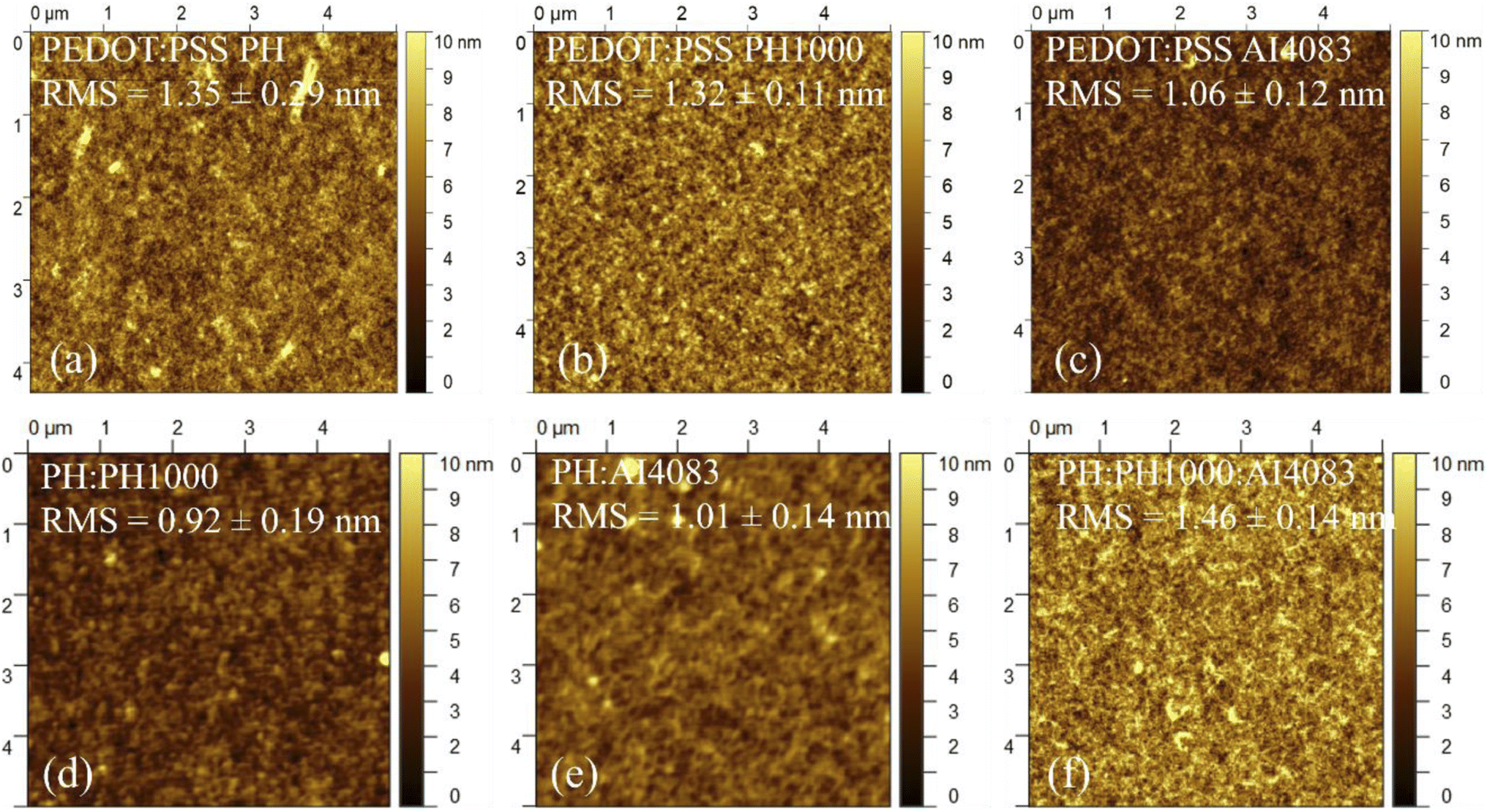 | ||
| Fig. 1 AFM height images of PEDOT:PSS thin films of (a) PH (b) PH1000, (c) AI4083, and their mixed PEDOT:PSS films of (d) PH:PH1000, (e) PH:AI4083, and (f) PH:PH1000:AI4083. | ||
It is confirmed that the substrate surface roughness and wettability properties regulate the nucleation and crystal growth of the perovskite layer deposited on it.38 Since MAPbI3−xClx films were deposited on top of PEDOT:PSS layers, the surface wettability of different PEDOT:PSS layers was also important to study. Hence, to estimate the PEDOT:PSS surface energy and polarity, we have conducted their water contact angle measurements for each PEDOT:PSS film. This is because the contact angle of a water drop is frequently used to evaluate surface properties.42 The measured contact angles of water droplets on the PEDOT:PSS layers shown in Fig. 2 are 19.6°, 37.6°, 14.7°, 23.7°, 11.7°, and 17.2° for PH, PH1000, AI4083, PH:PH1000, PH:AI4083 and PH:PH1000:AI4083, respectively.
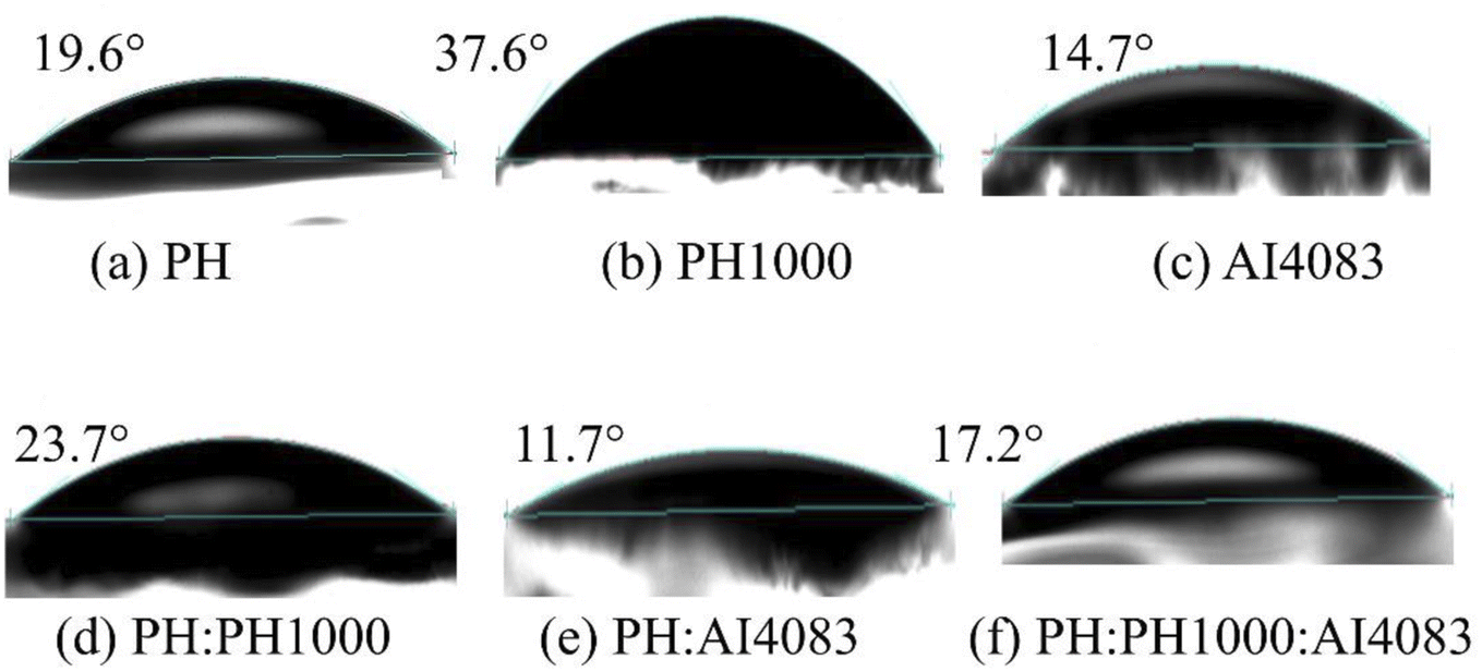 | ||
| Fig. 2 Photographs of the contact angle (CA) of water on different PEDOT:PSS films of (a) PH, (b) PH1000, (c) AI4083, and mixed PEDOT:PSS films of (d) PH:PH100, (e) PH:AI4083, and (f) PH:PH1000:AI4083. | ||
The wetting capability of different PEDOT:PSS surfaces to water is represented by the measured contact angle. As a result, we speculate that the MAPbI3−xClx film formed on these PEDOT:PSS layers, which was dissolved in the polar solvent N,N-dimethylformamide (DMF), will exhibit a similar surface wettability effect. As shown in Fig. 2b, the contact angle for PH1000 is higher than all other PEDOT:PSS films. It is reported that to improve the wettability of PH1000, Zonyl is often used as surfactant.43 And hence, it was difficult to fabricate continuous pinhole-free hydrophilic MAPbI3−xClx films on less-wetting PH1000 surfaces, which was further confirmed by the SEM images (see Fig. 3b below). Continuous PbI2 film formation on the HTLs is required for continuous final MAPbI3−xClx film formation.
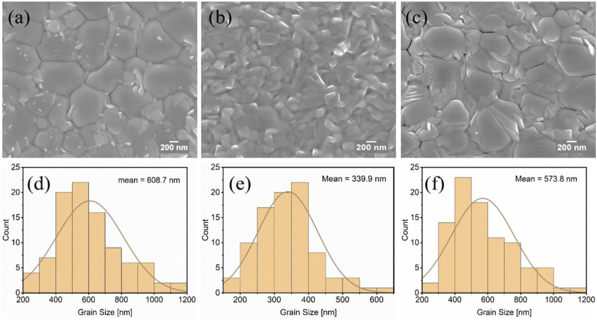 | ||
| Fig. 3 Top view of the SEM images of MAPbI3−xClx films on PEDOT:PSS (a) PH, (b) PH1000, (c) AI4083 layers, and (d–f) histogram showing the corresponding grain size distribution of all films. | ||
Crystallization and morphology of perovskite film
The microstructure of perovskite films produced on various PEDOT:PSS films was investigated using scanning electron microscopy (SEM). The top-view SEM images of the MAPbI3−xClx films in Fig. 3 and 4 show a clear relationship between different PEDOT:PSS surface wetting capabilities and grain morphology. The surface wettability, roughness, and composition of the PEDOT:PSS films may have contributed to significant morphological differences in the MAPbI3−xClx films.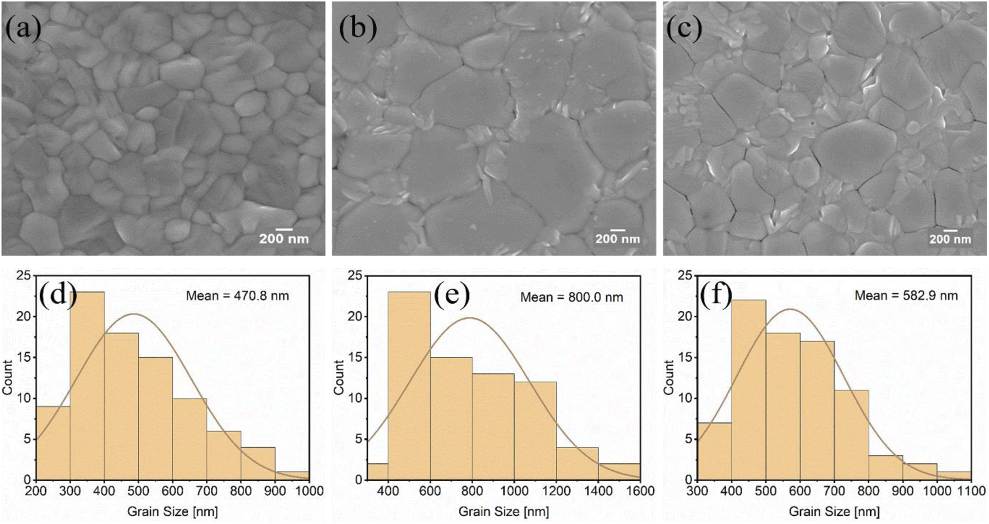 | ||
| Fig. 4 Top view of the SEM images of MAPbI3−xClx films on mixed PEDOT:PSS (a) PH:PH1000, (b) PH:AI4083, (c) PH:PH1000:AI4083 layers, and (d–f) histogram showing corresponding grain size distribution of all films. | ||
According to our investigation from the AFM images, the PH demonstrated a rougher surface (Fig. 1a) than PH1000 and AI4083, and therefore led to a large grain size of MAPbI3−xClx crystals with more homogenous grain distribution without pin holes as shown in Fig. 3a. But even though the PH1000 has a comparable RMS value, the MAPbI3−xClx film is characterized by small grain size and increased roughness (Fig. 3b). This is because the surface energy of PH1000 is completely different from the other PEDOT:PSS layers, which is characterized by a higher contact angle. As a result, PH1000 leads to a poor and small grain size of MAPbI3−xClx film formation and is usually processed with the addition of DMSO and Zynol.44 It is well known that the small grains of perovskite films act as recombination hot spots in perovskite solar cells.45 We have also calculated and compared the corresponding mean grain size of MAPbI3−xClx films. As it can be seen from Fig. 3d, the grain size on top of the PH layer is almost doubled that on top of the PH1000 layer (Fig. 3e).
Similarly, the effect of mixed PEDOT:PSS layers on the crystallization and morphology of MAPbI3−xClx films was also investigated. Significant morphological alterations in the crystallization of MAPbI3−xClx films have been found. The MAPbI3−xClx layers deposited on the mixed PEDOT:PSS (Fig. 4a–c) exhibited distinct features compared to those deposited on single formulation PEDOT:PSS layers. The average smallest grain size (470 nm) of MAPbI3−xClx was obtained on the PH:PH1000 layer (Fig. 4d), which, in agreement with its lower surface roughness and moderate contact angle, resulted in the most homogeneous appearance of the crystallites. The MAPbI3−xClx film produced on PH:AI4083, with better surface wettability and average roughness, exhibited a considerably larger average grain size of 800 nm (Fig. 4e). But the MAPbI3−xClx film deposited on the rougher surface PH:PH1000:AI4083 layer was in between the other two MAPbI3−xClx films deposited on PH:PH1000 and PH:AI4083, with an average grain size of 582 nm (Fig. 4f). As can be seen from Fig. 4, all the mixed PEDOT:PSS layers produced a very smooth morphology of MAPbI3−xClx films as compared to their counterparts single formulation PEDOT:PSS layers.
Hence, our pioneering work on mixing PEDOT:PSS with different formulations and properties has resulted in new PEDOT:PSS combinations with new properties. These are work functions, surface wettability, and surface roughness which are very important parameters for the perovskite crystallization and associated perovskite solar cell efficiency and stability. For example, we are successful in changing the bad wettability and lower work function of PEDOT:PSS PH1000 by adding PEDOT:PSS PH in a 1:1 ratio, while others used other chemicals like DMSO and Zonyl to modify its surface wettability problem.44
On top of the SEM measurements, to further understand the crystal quality and grain size of the perovskite films deposited and grown on the different PEDOT:PSS layers, X-ray diffraction (XRD) measurements (2theta–Ω-scan) were carried out. Fig. 5a and b compares the main characteristic XRD patterns of perovskite films on PEDOT:PSS (PH, PH1000, and AI4083) and on the mixed (PH:PH1000, PH:AI4083, and PH:PH1000:AI4083) layers respectively. We try to compare the grain size of MAPbI3−xClx by monitoring the full-width half maxima (FWHM) of the main peak (110). Accordingly, the FWHM of MAPbI3−xClx decreased from 0.1393°, 0.1324°, and 0.1293° for PH1000, AI4083, and PH respectively (Fig. 5a). The FWHM value of 0.1293° and its intense peak of MAPbI3−xClx on PH layer confirmed that the crystal quality is better as compared on the two PH1000 and AI4083 layers, which is consistent with the SEM results. This is because, the enhancement of peak intensity and decrease of FWHM value, suggested improved crystalline perovskite film.46,47 Similarly, the relatively smaller FWHM value (0.1246°) and peak intensity of MAPbI3−xClx film on PH:AI4083 showed better crystallization and grain size followed by three blend PEDOT:PSS as compared to the PH:PH1000 layer (Fig. 5b). And this is also in agreement with the SEM results. We have also calculated the single crystal grain size of MAPbI3−xClx using the Scherrer formula. And the values obtained are 68.4, 66.7, 68.6, 72.5, 74.0, and 73.4 nm for the PEDOT:PPS, PH, PH1000, AI4083, PH:PH1000, PH:AI4083, and PH:PH1000:AI4083 layers respectively. As shown in Fig. 5c, these values are in agreement with the average grain size obtained from the SEM measurements. The grain size values obtained from XRD are smaller as compared to the average grain size obtained from the SEM results. With SEM we see physical grains, while with XRD we calculate the size of the crystallites domains. A single grain can contain several domains with different orientations, so the size determined with SEM is always larger than what is determined by XRD.48
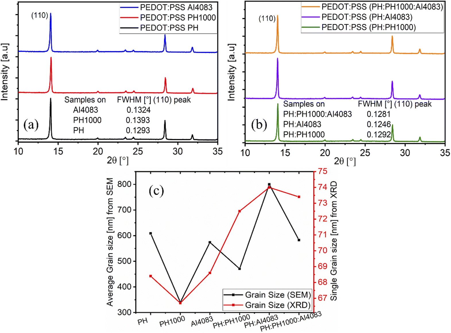 | ||
| Fig. 5 XRD patterns and FWHM values of the main peaks of MAPbI3−xClx films on (a) PEDOT:PSS (PH, PH1000, AI4083), and (b) on mixed PEDOT:PSS (PH:PH1000, PH:AI4983, PH:PH1000:AI4083), and (c) comparison of grain size of MAPbI3−xClx films from SEM and XRD measurements. | ||
Optical characterization of PEDOT:PSS layers and perovskite films
The optical transmittance spectra of the control and mixed PEDOT:PSS films cast on ITO–glass are shown in Fig. 6a and d respectively. At various wavelengths, the transmittance spectrum displays the fraction of incident light that passes through the sample without being absorbed, reflected, or scattered.39 As can be observed from Fig. 6a, the AI4083 has a higher transmittance, whilst the PH and PH1000 have similar but lower transmittance. The higher the transmittance, the more photons can reach the photoactive layer, increasing the likelihood of charge production. For AI4083 with a different pattern, there is a distinct transmittance increase around 550 nm. The transmittance of the mixed PEDOT:PSS, on the other hand, showed a similar pattern (Fig. 6d). Between the 550 and 800 nm wavelengths, the overall transmittance values of all PEDOT:PSS films employed here ranged from 75 to 85%. The ITO has higher light reflecting property as compared to the PEDOT:PSS layers in the range from 350 to 500 nm, and hence ITO has lower transmittance in that range.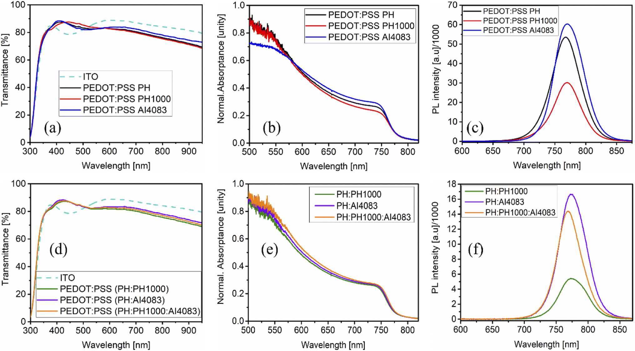 | ||
| Fig. 6 Transmittance of PEDOT:PSS (PH, PH1000, AI4083) films with ITO as reference (a), absorptance (b), and photoluminescence (c) spectra of MAPbI3−xClx films grown on those PEDOT:PSS films. And transmittance of mixed PEDOT:PSS (PH:PH1000, PH:AI4083, PH:PH1000:AI4083) films with ITO as reference (d), absorptance (e), and photoluminescence (f) spectra of MAPbI3−xClx films grown on the mixed PEDOT:PSS films. | ||
We subsequently evaluated the effect of the PEDOT:PSS layers on the optical features of the MAPbI3−xClx perovskite film, taking into account their nature and their significant influence on the morphology and crystallization of the perovskite film. The absorptance (Fig. 6b and e) and photoluminescence (PL) (Fig. 6c and f) spectra of MAPbI3−xClx perovskite films grown on each PEDOT:PSS layer were examined. All the absorptance spectra are comparable, exhibiting an absorption onset at 750 nm, corresponding to the bandgap transition of the perovskite family of MAPbI3.49 At 500 nm, a second transition occurs, which corresponds to the excitation of the lead-iodide octahedra PbI6.50 As shown in Fig. 6b, the perovskite layer on PH1000 has the lowest absorptance, indicating that the perovskite layer is of lower crystal quality, which is consistent with the SEM image and XRD results. However, the perovskite layer on the mixed PEDOT:PSS showed a similar absorptance pattern (Fig. 3e).
Upon excitation at 405 nm, the MAPbI3−xClx perovskite showed photoluminescence peaking between 760 and 775 nm. Intriguingly, blue shifting of the PL-peak indicates a decrease in the bandgap due to subsequent changes in the crystal structure that enhance orbital overlap between lead (Pb) and iodine (I) atoms.51,52 To large extent, the perovskite films deposited on PH and AI4083 revealed comparably blue-shifted but stronger PL emission intensity than the counterpart on PH1000 (Fig. 6c), confirming better crystallization of MAPbI3−xClx film. We also observed a considerable difference in the PL measurements carried out for MAPbI3−xClx films deposited on the mixed PEDOT:PSS layers. For MAPbI3−xClx film deposited on PH:PH1000 or PH:AI4083 layers (Fig. 6f), a broader and rather red-shifted PL-spectrum was detected in comparison to the film deposited on the triple-blend PEDOT:PSS layer. While the film on PH:AI4083 exhibited the highest photoluminescence emission, confirming better crystal quality as supported from SEM and XRD results.
Photovoltaic properties of inverted perovskite solar cells
To find the correlation between the wettability effect of PEDOT:PSS formulations and their mixtures used as HTL on the performance of perovskite devices, a series of inverted perovskite solar cells were fabricated. The via EQE corrected current–voltage (J–V) values of champion devices measured under near AM 1.5G illumination (100 mW cm−2) are shown in Fig. 7. As can be confirmed from the photovoltaic parameters depicted in Table 3, PH revealed the overall best performance followed by AI4083 among the three PEDOT:PSS formulations. And these results are in agreement with the larger grain crystals of MAPbI3−xClx films on PH and AI403 respectively. This is because increasing grain size and lowering grain boundaries in the perovskite film are known to be helpful for high open-circuit voltage and fill factor values.39 As expected, the device fabricated using PH1000 as HTL layer had a very low power conversion efficiency of 3.6%, equivalent to a short circuit current density (JSC) of 9.8 mA cm−2, open-circuit voltage (VOC) of 0.705 V, and fill factor (FF) of 52%. We furthermore noticed a very weak shunt resistance (462 Ω) to be related to the losses in the VOC and FF, in agreement with the report that, a device with a PH1000 layer was found to perform worse than AI4083.51 The lower VOC value for PH1000 can be explained by the very small grain sizes of MAPbI3−xClx film.53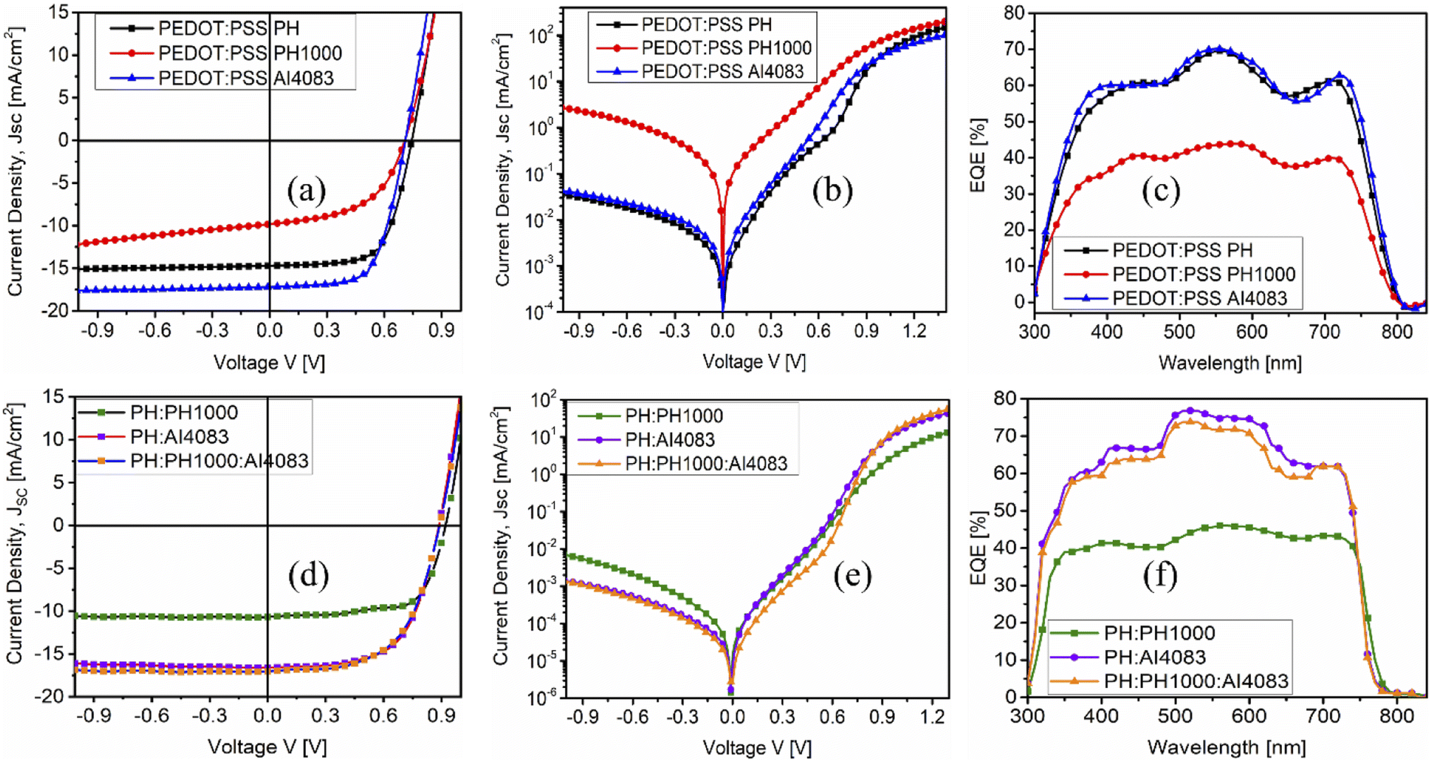 | ||
| Fig. 7 Characteristics of perovskite solar cells; (a) light J–V curve, (b) dark J–V curve, and (c) EQE spectra for the three PEDOT:PSS (PH, PH1000, AI4083). And (d) light J–V curve, (e) dark J–V curve, and (f) EQE spectra for the mixed PEDOT:PSS (PH:PH1000, PH:AI4083, PH:PH1000:AI4083) used as HTLs. | ||
| PEDOT:PSS as HTL | JSC,EQE (mA cm−2) | VOC (mV) | FF (%) | PCE corr. (%) | RS (Ω) | RP (Ω) |
|---|---|---|---|---|---|---|
| PH | 14.5 | 916 | 67 | 9.0 | 8 | 1326 |
| PH1000 | 9.8 | 705 | 52 | 3.6 | 6 | 462 |
| AI4083 | 17.3 | 750 | 59 | 7.7 | 10 | 1740 |
| PH:PH1000 | 8.9 | 954 | 65 | 5.5 | 8 | 1757 |
| PH:AI4083 | 14.5 | 905 | 62 | 8.1 | 9 | 2844 |
| PH:PH1000:AI4083 | 14.8 | 913 | 59 | 7.9 | 11 | 2591 |
Among the devices that used a mixture of PEDOT:PSS as HTLs, the device produced with PH:PH1000 layer had the lowest power conversion efficiency of 5.5%, equivalent to JSC of 8.9 mA cm−2, VOC of 0.954 V, and FF of 65%. Besides the higher VOC and FF, a considerably increased shunt resistance might be associated with the smooth morphology of the perovskite layer observed via SEM. All the devices employed mixed PEDOT:PSS is characterized by higher VOC and FF as compared to the pristine PEDOT:PSS layers.
The light, dark current–voltage characteristics and EQE spectra of the devices under investigation for the three control PEDOT:PSS layers are depicted in Fig. 7a–c. And the devices for the mixed PEDOT:PSS are displayed in Fig. 7d–f. The device with PH1000 had a very low parallel resistance (Table 3) and the highest reverse current (Fig. 7b) contributing to its lower performance. To understand the mechanism from the device's perspective, dark J–V curves were recorded. Both devices with PH and AI4083 exhibit normal diode behaviour and had a two order of magnitude lower leakage current than the device with PH1000. The same diode behaviour trend is also revealed by the devices that use the mixed layers, PH:AI4083 and PH:PH1000:AI4083 over the device with PH:PH1000 (Fig. 7e). The EQE spectra show rather similar onsets of the photocurrents at 800 nm, well corresponding to the bandgap of MAPbI3−xClx. The reduced (lower by nearly 30%), charge collection by PH1000, as revealed from EQE measurement (Fig. 7c), also suggests leakage currents. Devices with mixed PEDOT:PSS revealed comparable charge collection (Fig. 7f) except for PH:PH1000.
The lower performance associated with the device based on PH1000 layer might be due to its rough surface, leading to the inferior crystallization of perovskite.12 Without surprise, the higher conductivity of PH1000 (Table 1), is of no use for gaining higher power conversion efficiencies. For statistical comparison, we include the multiple battery photovoltaic parameters distribution (VOC, JSC, FF, and PCE) obtained under one sun simulated illumination, computed and plotted for 20 cells each (Fig. 8a and b). The trend observed for the best EQE corrected devices is confirmed also for a more considerable amount of devices. As can be seen from Fig. 8a, the performance of PH as HTL is leading followed by AI4083 as compared to that of PH1000. As reported in our previous work, PEDOT:PSS PH is also effective HTL with another perovskite material system (FAxMA1−xPbI3).54 For the mixed PEDOT:PSS layers (Fig. 8b), the PH:AI4083 and PH:PH100:AI4083 layers showed almost similar performance but better than PH:PH1000, showing consistency with SEM and XRD results.
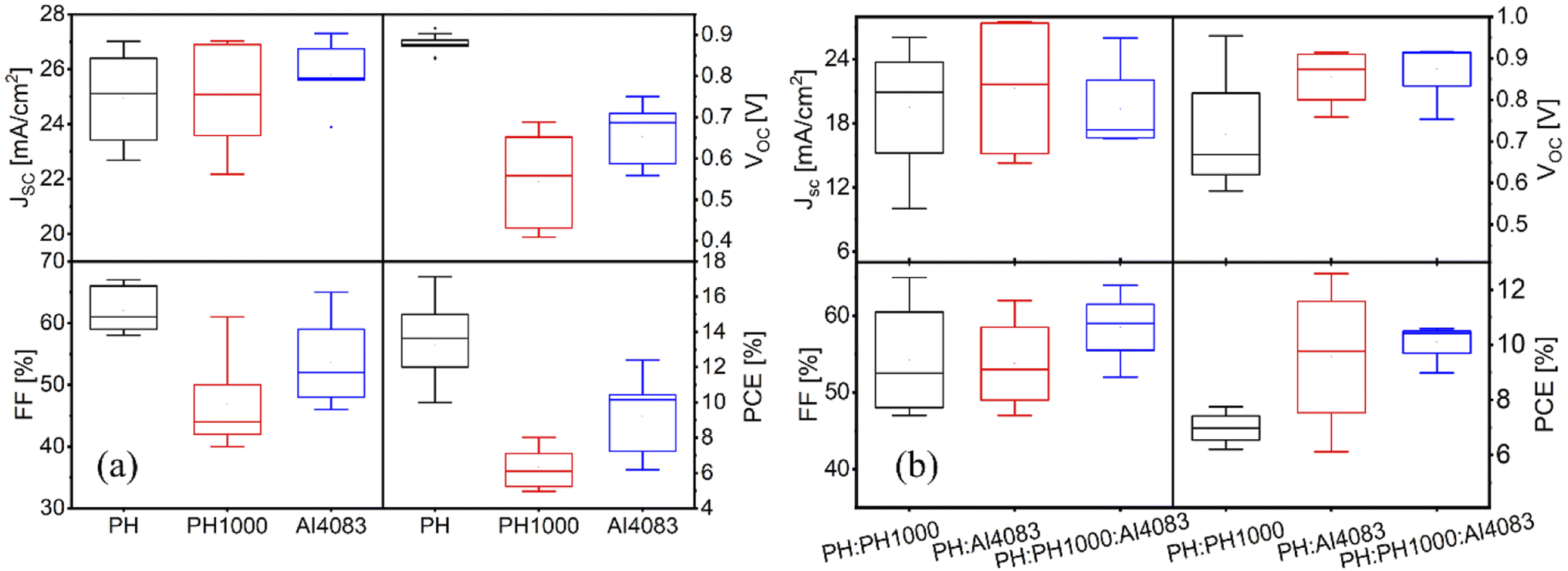 | ||
| Fig. 8 Statistical comparison of device performance between (a) PEDOT:PSS (PH, PH1000, AI4083), and (b) mixed PEDOT:PSS (PH:PH1000, PH:AI4083, PH:PH1000:AI4083) used as HTLs. | ||
The overall lower device performances in these studies as compared to using another HTL could be explained by the existing energy band gap misalignment of the PEDOT:PSS layers with the perovskite layer.55 For example, early research indicated that the content of PSS in different PEDOT:PSS formulations had a significant impact on the Fermi level of PEDOT:PSS towards higher work function.56 In this regard, there is one report that uses higher PSS content of ratio 1:20 (PEDOT to PSS), yielding high solar cell performance.18 On top of this, the efficiency of our devices is tested and reported based on a large active area of 0.42 cm2, whereas the reported efficiencies of PSC, in general, are based on an active area of roughly ≤0.1 cm2.2,57 Furthermore, the goal of this research is to investigate the impact of surface wettability of different PEDOT:PSS formulations and their mixtures on the perovskite crystallization and morphology, and demonstrate the corresponding device efficiency. Hence, the significance of surface tension force on grain nucleation and growth was validated by comparing grain morphological evolution of the MAPbI3−xClx films produced on the HTLs. Improved HTL/MAPbI3−xClx interface quality is also believed to aid in trap density reduction leading to a decrease in the nonradiative recombination losses.12
Conclusion
In this study, the crystal quality of perovskites and the performance of associated solar cells were examined by using three commercially available PEDOT:PSS formulations (PH, PH1000, and AI4083), and three mixtures thereof (PH:PH1000, PH:AI4083, and PH:PH1000:AI4083; in a 1:1 and 1:1:1 ratios) used as hole transport layers (HTLs). The optical, SEM, and XRD results have proved that the different PEDOT:PSS layers have influenced the crystal quality and grain size of the MAPbI3−xClx film differently. Of the three PEDOT:PSS formulations, PEDOT:PSS PH has shown better perovskite crystallization and higher corresponding solar cell performances. Differences in the device performance are expected to mainly result from differences in grain sizes of the perovskite layers. And the discrepancies in perovskite crystallization were attributed to the HTLs' varied surface wettability. We were also able to introduce mixed PEDOT:PSS layers with new work functions and new surface wettability that work effectively as HTLs for the first time. The idea of blending different PEDOT:PSS (with various mixing ratios) may open up the possibility of creating conductive layers with novel and easily tuneable features such as work functions, wettability, and conductivities for various optoelectronic applications. Although the three mixed PEDOT:PSS (PH:PH1000, PH:AI4083, and PH:PH1000:AI4083) layers have proved promising performances, they did not outperform the best single PEDOT:PSS PH. Relatively, the mixture of PH:AI4083 layer is performing better than the other two mixtures. In general, the mixture of different PEDOT:PSS formulations resulted in higher open-circuit voltage and fill factor values compared to the counter individual formulations also supported by the SEM and XRD results.
Conflicts of interest
We have no conflicts of interest to disclose.Acknowledgements
ZTG acknowledges for financial support by DAAD (Deutscher Akademischer Austauschdienst), funding programme/ID: 57299294. HH and USS are grateful to the Thüringer Ministerium für Wirtschaft, Wissenschaft und Digitale Gesellschaft (TMWWDG) for funding the CEEC Jena (RIS3 Innovation Center). The SEM facilities of the Jena Centre for Soft Matter (JCSM) were established with a grant from the Deutsche Forschungsgemeinschaft (DFG). The authors acknowledges Dr Stephanie Höppener for the AFM, and Aman Anand for the work functions measurements of the PEDOT:PSS films.References
- W. Han, G. Ren, J. Liu, Z. Li, H. Bao, C. Liu and W. Guo, ACS Appl. Mater. Interfaces, 2020, 12, 49297–49322 CrossRef CAS.
- T. Wu, Z. Qin, Y. Wang, Y. Wu, W. Chen, S. Zhang, M. Cai, S. Dai, J. Zhang, J. Liu, Z. Zhou, X. Liu, H. Segawa, H. Tan, Q. Tang, J. Fang, Y. Li, L. Ding, Z. Ning, Y. Qi, Y. Zhang and L. Han, Nano-Micro Lett., 2021, 13, 152 CrossRef CAS.
- Best research-cell efficiency chart of NREL, Golden Colorado, 2022 Search PubMed.
- F. Li, X. Deng, F. Qi, Z. Li, D. Liu, D. Shen, M. Qin, S. Wu, F. Lin, S. H. Jang, J. Zhang, X. Lu, D. Lei, C. S. Lee, Z. Zhu and A. K. Jen, J. Am. Chem. Soc., 2020, 142, 20134–20142 CrossRef CAS PubMed.
- Y. Wu, D. Wang, J. Liu and H. Cai, Nanomaterials, 2021, 11, 755 CrossRef PubMed.
- J. Jeong, M. Kim, J. Seo, H. Lu, P. Ahlawat, A. Mishra, Y. Yang, M. A. Hope, F. T. Eickemeyer, M. Kim, Y. J. Yoon, I. W. Choi, B. P. Darwich, S. J. Choi, Y. Jo, J. H. Lee, B. Walker, S. M. Zakeeruddin, L. Emsley, U. Rothlisberger, A. Hagfeldt, D. S. Kim, M. Gratzel and J. Y. Kim, Nature, 2021, 592, 381–385 CrossRef CAS.
- A. Sharenko and M. F. Toney, J. Am. Chem. Soc., 2016, 138, 463–470 CrossRef CAS.
- H. Mehdi, M. Matheron, A. Mhamdi, S. Cros and A. Bouazizi, J. Mater. Sci.: Mater. Electron., 2021, 32, 21579–21589 CrossRef CAS.
- C. A. Aranda, L. Caliò and M. Salado, Crystals, 2021, 11, 519 CrossRef CAS.
- T. Liu, K. Chen, Q. Hu, R. Zhu and Q. Gong, Adv. Energy Mater., 2016, 6, 1600457 CrossRef.
- A. Raj, M. Kumar and A. Anshul, Mater. Today Chem., 2021, 22, 100595 CrossRef CAS.
- C. Bi, Q. Wang, Y. Shao, Y. Yuan, Z. Xiao and J. Huang, Nat. Commun., 2015, 6, 7747 CrossRef CAS.
- T. Hu, F. Zhang, H. Yu, M. Zhang, Y. Yu, W. Zhang, R. Liu, L. Tian and Z. Ma, Nano Res., 2021, 14, 3864–3872 CrossRef CAS.
- M. N. Gueye, A. Carella, J. Faure-Vincent, R. Demadrille and J.-P. Simonato, Prog. Mater. Sci., 2020, 108, 100616 CrossRef CAS.
- S.-I. Na, G. Wang, S.-S. Kim, T.-W. Kim, S.-H. Oh, B.-K. Yu, T. Lee and D.-Y. Kim, J. Mater. Chem., 2009, 19, 9045 RSC.
- J. Y. Jeng, Y. F. Chiang, M. H. Lee, S. R. Peng, T. F. Guo, P. Chen and T. C. Wen, Adv. Mater., 2013, 25, 3727–3732 CrossRef CAS PubMed.
- N. Cheng, Z. Liu, Z. Yu, W. Li, Z. Zhao, Z. Xiao, B. Lei, S. Sun and W. Zi, Org. Electron., 2021, 98, 106298 CrossRef CAS.
- S. H. Chang, K.-F. Lin, K. Y. Chiu, C.-L. Tsai, H.-M. Cheng, S.-C. Yeh, W.-T. Wu, W.-N. Chen, C.-T. Chen, S.-H. Chen and C.-G. Wu, Sol. Energy, 2015, 122, 892–899 CrossRef CAS.
- F. Ongul, S. A. Yuksel, M. Kazici, S. Bozar, A. Gunbatti and S. Gunes, Polym. Adv. Technol., 2017, 28, 947–951 CrossRef CAS.
- A. Anand, J. P. Madalaimuthu, M. Schaal, F. Otto, M. Gruenewald, S. Alam, T. Fritz, U. S. Schubert and H. Hoppe, ACS Appl. Electron. Mater., 2021, 3, 929–943 CrossRef CAS.
- Y.-J. Xing, M.-F. Qian, D.-Z. Guo and G.-M. Zhang, Chin. Phys. B, 2014, 23, 038504 CrossRef CAS.
- T.-W. Lee and Y. Chung, Adv. Funct. Mater., 2008, 18, 2246–2252 CrossRef CAS.
- C.-J. Huang, K.-L. Chen, Y.-J. Tsao, D.-W. Chou, W.-R. Chen and T.-H. Meen, Synth. Met., 2013, 164, 38–41 CrossRef CAS.
- P.-W. Sze, K.-W. Lee, P.-C. Huang, D.-W. Chou, B.-S. Kao and C.-J. Huang, Energies, 2017, 10, 716 CrossRef.
- Q. Wang, B. Chen, Y. Liu, Y. Deng, Y. Bai, Q. Dong and J. Huang, Energy Environ. Sci., 2017, 10, 516–522 RSC.
- N. Ahn, K. Kwak, M. S. Jang, H. Yoon, B. Y. Lee, J. K. Lee, P. V. Pikhitsa, J. Byun and M. Choi, Nat. Commun., 2016, 7, 13422 CrossRef CAS PubMed.
- N. Rolston, A. D. Printz, J. M. Tracy, H. C. Weerasinghe, D. Vak, L. J. Haur, A. Priyadarshi, N. Mathews, D. J. Slotcavage, M. D. McGehee, R. E. Kalan, K. Zielinski, R. L. Grimm, H. Tsai, W. Nie, A. D. Mohite, S. Gholipour, M. Saliba, M. Grätzel and R. H. Dauskardt, Adv. Energy Mater., 2017, 8, 1702116 CrossRef.
- C. Kan, Z. Tang, Y. Yao, P. Hang, B. Li, Y. Wang, X. Sun, M. Lei, D. Yang and X. Yu, ACS Energy Lett., 2021, 3864–3872, DOI:10.1021/acsenergylett.1c02030.
- M. M. Tepliakova, A. N. Mikheeva, P. A. Somov, E. S. Statnik, A. M. Korsunsky and K. J. Stevenson, Energies, 2021, 14, 5115 CrossRef CAS.
- D. B. Khadka, Y. Shirai, M. Yanagida and K. Miyano, ACS Appl. Energy Mater., 2021, 4, 11121–11132 CrossRef CAS.
- Y. Zhai, F. Li, M. Guo and C. Chen, J. Nanopart. Res., 2017, 19, 384 CrossRef.
- S. A. Thomas, J. C. Hamill Jr, S. J. O. White and Y. L. Loo, Adv. Mater. Interfaces, 2021, 8, 2100505 CrossRef CAS.
- S. T. Williams, C. C. Chueh and A. K. Jen, Small, 2015, 11, 3088–3096 CrossRef CAS.
- Q. Niu, W. Huang, J. Tong, H. Lv, Y. Deng, Y. Ma, Z. Zhao, R. Xia, W. Zeng, Y. Min and W. Huang, Synth. Met., 2018, 243, 17–24 CrossRef CAS.
- S. H. Park, A. Roy, S. Beaupré, S. Cho, N. Coates, J. S. Moon, D. Moses, M. Leclerc, K. Lee and A. J. Heeger, Nat. Photonics, 2009, 3, 297–302 CrossRef CAS.
- R. Roesch, K.-R. Eberhardt, S. Engmann, G. Gobsch and H. Hoppe, Sol. Energy Mater. Sol. Cells, 2013, 117, 59–66 CrossRef CAS.
- M. S. G. Hamed and G. T. Mola, Crit. Rev. Solid State Mater. Sci., 2019, 1–28, DOI:10.1080/10408436.2018.1549976.
- M. Pylnev, A. M. Barbisan and T.-C. Wei, Appl. Surf. Sci., 2021, 541, 148559 CrossRef CAS.
- H. M. Alishah, F. P. G. Choi and S. Gunes, J. Mater. Sci.: Mater. Electron., 2021, 32, 21450–21461 CrossRef CAS.
- Q. Wang, C. C. Chueh, M. Eslamian and A. K. Jen, ACS Appl. Mater. Interfaces, 2016, 8, 32068–32076 CrossRef CAS PubMed.
- J. P. Thomas, L. Zhao, D. McGillivray and K. T. Leung, J. Mater. Chem. A, 2014, 2, 2383 RSC.
- C. Caddeo, D. Marongiu, S. Meloni, A. Filippetti, F. Quochi, M. Saba and A. Mattoni, Adv. Mater. Interfaces, 2018, 1801173, DOI:10.1002/admi.201801173.
- M. M. Voigt, R. C. I. Mackenzie, C. P. Yau, P. Atienzar, J. Dane, P. E. Keivanidis, D. D. C. Bradley and J. Nelson, Sol. Energy Mater. Sol. Cells, 2011, 95, 731–734 CrossRef CAS.
- G. Adam, M. Kaltenbrunner, E. D. Głowacki, D. H. Apaydin, M. S. White, H. Heilbrunner, S. Tombe, P. Stadler, B. Ernecker, C. W. Klampfl, N. S. Sariciftci and M. C. Scharber, Sol. Energy Mater. Sol. Cells, 2016, 157, 318–325 CrossRef CAS.
- Q. An, F. Paulus, D. Becker-Koch, C. Cho, Q. Sun, A. Weu, S. Bitton, N. Tessler and Y. Vaynzof, Matter, 2021, 4, 1683–1701 CrossRef CAS.
- L. Han, S. Cong, H. Yang, Y. Lou, H. Wang, J. Huang, J. Zhu, Y. Wu, Q. Chen, B. Zhang, L. Zhang and G. Zou, Sol. RRL, 2018, 2, 1800054 CrossRef.
- J. Feng, X. Zhu, Z. Yang, X. Zhang, J. Niu, Z. Wang, S. Zuo, S. Priya, S. F. Liu and D. Yang, Adv. Mater., 2018, 30, e1801418 CrossRef PubMed.
- L. A. Muscarella, E. M. Hutter, S. Sanchez, C. D. Dieleman, T. J. Savenije, A. Hagfeldt, M. Saliba and B. Ehrler, J. Phys. Chem. Lett., 2019, 10, 6010–6018 CrossRef CAS.
- T. J. Jacobsson, J. P. Correa-Baena, E. Halvani Anaraki, B. Philippe, S. D. Stranks, M. E. Bouduban, W. Tress, K. Schenk, J. Teuscher, J. E. Moser, H. Rensmo and A. Hagfeldt, J. Am. Chem. Soc., 2016, 138, 10331–10343 CrossRef CAS PubMed.
- A. Khorasani, M. Marandi, A. Iraji zad and N. Taghavinia, Electrochim. Acta, 2019, 297, 1071–1078 CrossRef CAS.
- L. Hu, K. Sun, M. Wang, W. Chen, B. Yang, J. Fu, Z. Xiong, X. Li, X. Tang, Z. Zang, S. Zhang, L. Sun and M. Li, ACS Appl. Mater. Interfaces, 2017, 9, 43902–43909 CrossRef CAS.
- A. R. Marshall, H. C. Sansom, M. M. McCarthy, J. H. Warby, O. J. Ashton, B. Wenger and H. J. Snaith, Sol. RRL, 2020, 5, 2000599 CrossRef.
- K. G. Lim, H. B. Kim, J. Jeong, H. Kim, J. Y. Kim and T. W. Lee, Adv. Mater., 2014, 26, 6461–6466 CrossRef CAS.
- Z. T. Gebremichael, S. Alam, S. Stumpf, M. Diegel, U. S. Schubert and H. Hoppe, Nano Sel., 2022, 0, 1–11 Search PubMed.
- C. Xu, Z. Liu and E.-C. Lee, J. Mater. Chem. C, 2018, 6, 6975–6981 RSC.
- X. Lin, D. Cui, X. Luo, C. Zhang, Q. Han, Y. Wang and L. Han, Energy Environ. Sci., 2020, 13, 3823–3847 RSC.
- M. Yi, W. Jang and D. H. Wang, ACS Sustainable Chem. Eng., 2019, 7, 8245–8254 CrossRef CAS.
| This journal is © The Royal Society of Chemistry 2022 |