
 Open Access Article
 This Open Access Article is licensed under a
 Creative Commons Attribution 3.0 Unported Licence
Electric field tunability of the electronic properties and contact types in the MoS2/SiH heterostructure†
Son-Tung Nguyena,
Chuong V. Nguyen b,
Kien Nguyen-Bac,
Huy Le-Quoc*c,
Nguyen V. Hieud and
Cuong Q. Nguyen*ef
b,
Kien Nguyen-Bac,
Huy Le-Quoc*c,
Nguyen V. Hieud and
Cuong Q. Nguyen*ef
aFaculty of Electrical Engineering, Hanoi University of Industry, Hanoi 100000, Vietnam
bDepartment of Materials Science and Engineering, Le Quy Don Technical University, Hanoi, Vietnam
cThe University of Danang – University of Science and Technology, Danang 550000, Vietnam. E-mail: lqhuy@dut.udn.vn
dPhysics Department, The University of Danang – University of Science and Education, Da Nang 550000, Vietnam
eInstitute of Research and Development, Duy Tan University, Da Nang 550000, Vietnam. E-mail: nguyenquangcuong3@duytan.edu.vn
fFaculty of Natural Sciences, Duy Tan University, Da Nang 550000, Vietnam
First published on 25th August 2022
Abstract
The generation of layered heterostructures with type-II band alignment is considered to be an effective tool for the design and fabrication of a highly efficient photocatalyst. In this work, we design a novel type-II MoS2/SiH HTS and investigate its atomic structure, electronic properties and contact types. In the ground state, the MoS2/SiH HTS is proved to be structurally and mechanically stable. The MoS2/SiH HTS generates type-II band alignment with separation of the photogenerated carriers. Both the electronic properties and contact type of the MoS2/SiH HTS can be modulated by an external electric field. The application of a negative electric field leads to a transformation from type-II to type-I band alignment. While the application of a positive electric field gives rise to a transition from semiconductor to metal in the MoS2/SiH HTS. These results could provide useful information for the design and fabrication of photoelectric devices on the MoS2/SiH HTS.
1 Introduction
The successful isolation of graphene1 has opened up a new research direction in novel materials science. Over nearly one decade, a series of two-dimensional materials2–4 have been discovered, synthesized experimentally and investigated systematically. 2D materials are proved to have outstanding physical and chemical properties that make them promising candidates for various applications, including transistors,5 Li-ion batteries,6 water splitting7 and gas sensors.8 Graphene,1 hexagonal boron nitride (h-BN),9 transition metal dichalcogenides (TMDs)10 and phosphorene analogues11,12 are currently considered to be the most attractive 2D materials owing to their intriguing properties and wide range of applications. Although these 2D materials have promising properties, they also exhibit some disadvantages that may limit their applications in various fields. For instance, the lack of band gap in graphene13 limits its application in field-effect transistors.14 Unlike graphene, phosphorene is a semiconductor with a finite band gap. However, the structural instability under ambient conditions of phosphorene limits its application in modern day devices.15 Therefore, the search for novel 2D materials as well as finding common approaches to control their properties for various applications is still challenging.Currently, one of the most commonly used techniques to improve the properties and expand the application range of 2D materials is the generation of van der Waals (vdW) heterostructures (HTSs) between two or more different 2D materials.16,17 The different 2D materials in their vdW-HTSs are held together by the weak vdW forces. Thus, the intrinsic excellent properties of the constituent 2D materials are maintained in their combined HTSs. Moreover, the formation of vdW-HTSs between 2D materials may also give rise to the creation of novel properties that may not exist in the constituent 2D monolayers. Generally, the recombination of the photogenerated carriers in single-layer 2D materials is very rapid. Whereas, the photogenerated carriers in the combined vdW-HTSs between different 2D materials are separated effectively depending on the positions of the band edges of the constituent monolayers. The combination between two different 2D materials results in the formation of type-I, type-II or type-III band alignment, as depicted in Fig. S1 of the ESI.† For type-I, the conduction band minimum (CBM)/valence band maximum (VBM) of one layer is higher/lower than that of the other layer. In type-II, the CBM and VBM of the heterostructure come from different constituent monolayers. In type-III, the CBM of one layer is lower than the VBM of the other layer. To date, a large number of HTSs have been formed between two or more different 2D materials, such as graphene HTSs18–21 and TMD HTSs.22–25 The combination between two or more different 2D materials may also give rise to the appearance of novel properties that may not be observed in the 2D monolayers.
Recently, a novel 2D material, namely silane (SiH), was obtained by the covalent modification of hydrogen and silicene.26,27 Unlike silicene, the SiH monolayer is a semiconductor with a band gap of about 2.19 eV,28 making it suitable for photocatalysis and optoelectronic applications.29,30 The SiH monolayer is structurally stable at room temperature. The combination between the SiH monolayer and other 2D materials has been proposed and predicted recently. For instance, Han et al. investigated type-II band alignment in the GaAs/SiH HTS using first principles calculations.31 The results showed that the formation of the type-II GaAs/SiH HTS leads to an enhancement of the optical absorption in the visible light region. Zeng et al.29 constructed a novel SiH/CeO2(111) HTS and investigated its electronic and optical properties and photocatalytic performance. The results demonstrated that the novel SiH/CeO2(111) HTS generates type-II band alignment and it is a promising photocatalyst for splitting water to hydrogen. All the above-mentioned findings suggest that the SiH monolayer can be used to form HTSs with other 2D materials. Currently, MoS2 is one of the most attractive materials in the 2D TMD family.32 HTSs between MoS2 and other 2D materials have not only been predicted theoretically33,34 but also synthesized experimentally.35–37 However, to date, the combination between single layer SiH and MoS2 monolayers has not yet been designed and investigated.
In this work, we perform first principles calculations to design a novel MoS2/SiH HTS and investigate its atomic structure, electronic properties and contact types. Our results show that the MoS2/SiH HTS is structurally and mechanically stable in the ground state. The MoS2/SiH HTS generates type-II band alignment, making it a promising candidate as an efficient photovoltaic device because the photogenerated carriers in type-II are separated in the two materials. Both the electronic properties and contact type of the MoS2/SiH HTS can be modulated by an external electric field. The application of a negative electric field leads to a transformation from type-II to type-I band alignment. While the application of a positive electric field gives rise to a transition from semiconductor to metal in the MoS2/SiH HTS. These results could provide useful information for the design and synthesis of photocatalytic devices based on the MoS2/SiH HTS.
2 Computational methods
All calculations are performed in the framework of density functional theory (DFT) using first-principles calculations.38 The Vienna ab initio simulation (VASP)39,40 is used to perform the structural optimization and electronic properties prediction. The Perdew–Burke–Ernzerhof (PBE) functional in the framework of the generalized gradient approximation (GGA)41,42 is used to describe the exchange–correlation force. The HSE06 functional is chosen to obtain more accurately the band gaps of the materials.43 A vacuum space of 20 Å is used to avoid all unnecessary neighboring layered interactions in materials. A k-point mesh of 12 × 12 × 1 and a cut-off energy of 510 eV are chosen. All structural geometries are fully optimized until the convergence tolerance of energy and force which are less than 10−6 eV and 10−3 eV Å−1, respectively. A DFT-D3 method44 is also adopted to describe the long-range forces in the layered 2D materials.3 Results and discussion
We first investigate the atomic structure and electronic properties of MoS2 and SiH monolayers. The atomic structures of these monolayers are depicted in Fig. 1(a) and (e). The lattice constants of MoS2 and SiH monolayers after the geometric optimization are calculated to be 3.18 and 3.86 Å, respectively. These values are in good agreement with the previous reports.26,29,45–47 The band structures of MoS2 and SiH monolayers obtained by the PBE and HSE functionals are depicted in Fig. 1(b), (c), (f) and (g). Both the MoS2 and SiH monolayers are semiconductors with the band gap values of 1.78/2.26 and 2.18/2.93 eV obtained with the PBE/HSE functional, respectively. The MoS2 monolayer possesses a direct band gap with conduction band minimum (CBM) and valence band maximum (VBM) at the K point. Whereas, the SiH monolayer exhibits an indirect band gap with the VBM at the Γ point and the CBM at the M point. Both the PBE and HSE functionals predict the same characteristics of MoS2 and SiH monolayers, suggesting that the PBE method predicts the correct trends and physical mechanisms for the MoS2/SiH heterostructure. Thus, we decide to choose the PBE functional for all the next calculations because of a low computational cost. Moreover, our goal is not to acquire the precise band gaps of the MoS2/SiH heterostructure, but to explore the trend in electronic properties and contact types under external factors, such as external electric field.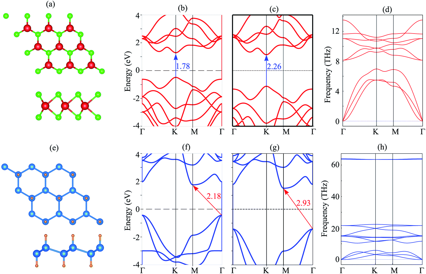 | ||
| Fig. 1 (a and e) The relaxed atomic structures, (b and f) PBE band structure, (c and g) HSE band structure and (d and h) phonon spectrum of the MoS2/SiH layer. | ||
We next design the combination between two different MoS2 and SiH monolayers to form the MoS2/SiH heterostructure. We designed five different stacking configurations of the MoS2/SiH heterostructure. The most energetically stable stacking configuration of the MoS2/SiH heterostructure is shown in Fig. 2, while the other stacking configurations are illustrated in Fig. S2 of the ESI.† It should be noted that the stacking configuration of the MoS2/SiH heterostructure presented in the manuscript is the most energetically stable heterostructure because it has the lowest binding energy compared to the others. In order to design the MoS2/SiH heterostructure, we use a supercell, consisting of (2 × 2) unit cells of the MoS2 layer and 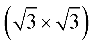 unit cells of the SiH monolayer. The lattice constant of the MoS2/SiH heterostructure after geometric optimization is found to be 6.43 Å. The lattice mismatch in the MoS2/SiH heterostructure is calculated to be less than 2%, which is small and affects insignificantly the electronic features of the heterostructure. After geometric optimization, the interlayer spacing between MoS2 and SiH layers in the corresponding heterostructure is 2.48 Å. This interlayer spacing is in the same order of magnitude as other Si(Ge)H-based heterostructures, such as GeH/graphene,48 SiH/PtSe2,47 and SiH/AlAs.49 Moreover, to check the structural stability of such a heterostructure, we further calculate the binding energy as: Eb = [EH − (EM − ES)]/A, where EH, EM and ES are the total energies of the MoS2/SiH heterostructure, and isolated MoS2 and SiH monolayers, respectively. A is the surface area of the MoS2/SiH HTS. The binding energy of the MoS2/SiH HTS is −11.44 meV Å−2. The negative sign of the binding energy implies that the MoS2/SiH HTS is stable at the equilibrium interlayer spacing. Moreover, to check the mechanical stability of such a HTS, we also calculate the elastic constants of the MoS2/SiH HTS. The elastic constants [Cij] of the MoS2/SiH HTS include four components, namely C11, C12, C22 and C66. The MoS2/SiH HTS is mechanically stable when its elastic constants satisfy the Born–Huang criteria,50 i.e. C66 > 0 and C11C22 − C122 > 0. Our calculated elastic constants of the MoS2/SiH HTS are C11 = C22 = 188.37 N m−1, C12 = 48.29 N m−1 and C66 = 70.06 N m−1. These values of the elastic constants of the MoS2/SiH HTS indicate that it is mechanically stable.
 | ||
| Fig. 2 (a) Top view and (b) side view of the most energetically stable stacking configuration of the MoS2/SiH HTS. The supercell of the considered HTS is marked by a black line. | ||
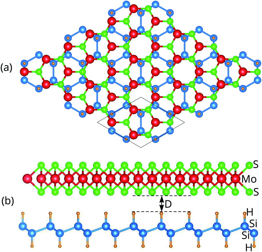
The projected band structure of the MoS2/SiH HTS is illustrated in Fig. 3(a). The contributions of MoS2 and SiH layers are represented by blue and red circles, respectively. One can find that the MoS2/SiH HTS possesses a semiconducting nature with an indirect band gap of 0.26 eV, which is smaller than that of both the MoS2 and SiH monolayers. This finding indicates that the generation of the MoS2/SiH HTS gives rise to a reduction in the band gap compared to that of the constituent monolayers. More interestingly, the VBM of the MoS2/SiH HTS is located at the Γ point and it comes mainly from the SiH layer. Whereas, the CBM of the MoS2/SiH HTS is located at the M point and it is mainly contributed by the MoS2 layer. These contributions demonstrate that the VBM and CBM of the MoS2/SiH HTS come from different layers, resulting in the formation of type-II band alignment. The type-II band alignment of the MoS2/SiH HTS makes it a promising candidate as an efficient photovoltaic device because the photogenerated carriers in type-II are separated in the two materials.
 | ||
| Fig. 3 (a) Projected band structure, (b) plane-averaged charge density difference and (c) electrostatic potential of the MoS2/SiH HTS. The red and blue circles in (a) represent the contributions of SiH and MoS2 layers, respectively. The inset in (b) is the 3D charge density difference. Cyan and yellow regions represent the gain and loss of electrons, respectively. | ||
The generation of type-II band alignment in the MoS2/SiH HTS may lead to charge redistribution at the interface. Therefore, we further visualize the charge density difference as Δρ = ρH − ρM − ρS, where ρH, ρM and ρS are the charge densities of the MoS2/SiH HTS, and isolated MoS2 and SiH monolayers, respectively. One can observe from Fig. 3(b) that there is a charge redistribution at the interface of the MoS2/SiH HTS. In addition, we find that the SiH layer loses electrons, while the MoS2 layer gains electrons. This indicates that the charges are transferred from SiH to MoS2 layers in the MoS2/SiH HTS. Furthermore, the electrostatic potential of the MoS2/SiH HTS in Fig. 3(c) demonstrates that the MoS2 layer has a deeper potential than the SiH layer, causing the creation of a built-in electric field. The potential drop between the MoS2 and SiH layers is 4.2 eV. It is obvious that the formation of a built-in electric field at the interface of the MoS2/SiH HTS gives rise to the separation of the photogenerated electrons and holes as well as the inhibition of their recombination.
Furthermore, to have a better understanding of the charge transfer between two different MoS2 and SiH layers, we calculate the work function of the MoS2/SiH HTS as well as the constituent MoS2 and SiH monolayers for comparison. The work function can be calculated as: Φ = Evac − EF, where Evac and EF are the vacuum energy and the Fermi level energy, respectively. The calculated work functions of the MoS2/SiH HTS, and isolated MoS2 and SiH monolayers are 4.62, 5.15 and 5.80 eV, respectively. The difference in the work functions of the MoS2 and SiH monolayers allows the charge transfer from the SiH to the MoS2 layer. Furthermore, the work function of the MoS2/SiH HTS is lower than that of both the MoS2 and SiH monolayers, suggesting that there is a charge redistribution at the interface of the heterostructure.
Currently, applying an electric field (E) is proven to be an effective tool to modify the electronic properties and contact types in the HTS between two different 2D materials. The strength of the applied E ranges from −0.4 V Å−1 to +0.4 V Å−1. The direction of the applied E is from the SiH to the MoS2 layer, as depicted in Fig. 4(a). It should be noted that the electric field was applied for both the optimization process and electronic properties calculations. Our results showed that the relaxed atomic structures of the MoS2/SiH heterostructure remain unchanged when the electric field is applied in the optimization process as compared to those without the application of the electric field, as depicted in Fig. S3 of the ESI.† The dependence of the band gap of the MoS2/SiH HTS as a function of applied E is depicted in Fig. 4(b). One can find that a positive E leads to a narrower band gap of the MoS2/SiH HTS, while a negative E gives rise to an increase in the band gap of the MoS2/SiH HTS. Under the positive E = +0.4 V Å−1, the band gap of the MoS2/SiH HTS is reduced to zero, indicating that the semiconducting nature in the MoS2/SiH HTS transforms into metallic nature. Moreover, it is obvious that the band gap changes of the MoS2/SiH HTS may be related to a change in the band edges of the constituent monolayers. Thus, in order to have a better understanding of the physical nature of the modulation of the band gap by the application of the E, we plot the positions of the VBM and CBM band edges of the constituent MoS2 and SiH monolayers under different values of negative and positive E, as illustrated in Fig. 4(c) and (d), respectively. From these figures, one can find that the CBM (VBM) value of the SiH (MoS2) layer is increased when the applied E is changed from −0.4 to +0.4 V Å−1. On the other hand, the VBM (CBM) of the SiH (MoS2) layer decreases correspondingly. As we have discussed above, type-II band alignment is formed in the MoS2/SiH HTS with the contribution of the SiH layer to the VBM and the contribution of the MoS2 layer to the CBM. The decrease in the VBM value of the SiH layer and the CBM value of the MoS2 layer when the applied E is changed from −0.4 V Å−1 to +0.4 V Å−1 leads to a narrower band gap of the MoS2/SiH HTS.
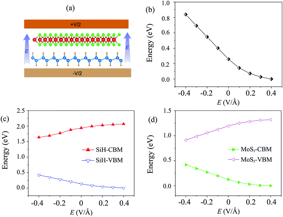 | ||
| Fig. 4 (a) Schematic model of applied-E to the MoS2/SiH HTS. The variations of (b) the band gap and the band edges of (c) SiH and (d) MoS2 layers as a function of electric field. | ||
Furthermore, to further comprehend the effect of electric field on the band gap of the MoS2/SiH HTS, we plot its projected band structures under different strengths of applied E, as depicted in Fig. 5. When a negative E is applied, the VBM (CBM) of the SiH layer shifts away from (towards) the Fermi level of the HTS. Whereas, the VBM (CBM) of the MoS2 layer shifts towards (away from) the Fermi level of the HTS. This trend shows that under the application of the negative E, the VBM of the SiH layer and the CBM of MoS2 shift away from the Fermi level, giving rise to an increase in the band gap of the MoS2/SiH HTS. Furthermore, under the application of the positive E, the movement of the VBM and CBM of the MoS2 and SiH layers in the corresponding MoS2/SiH HTS is in the opposite direction compared with the applied negative E. Thus, the positive E leads to a reduction of the band gap of the MoS2/SiH HTS. Under the application of the positive E = +0.4 V Å−1, both the VBM and CBM of the MoS2/SiH HTS cross the Fermi level, indicating a transformation from semiconductor to metal. Moreover, following the changing trend in the band edges of the MoS2 and SiH layers in the corresponding MoS2/SiH HTS, we predict that the VBM of the SiH layer will be lower than that of MoS2 at the critical strength of the negative E = −0.7 V Å−1. This prediction suggests that a transformation from type-II to type-I band alignment will be achieved under the application of a negative electric field of −0.7 V Å−1. However, it would not be reasonable to apply higher E values, since they would be rather difficult to experimentally achieve. In addition, it should be noted that to apply an electric field in devices, experimental realization is considered as one pole of the battery connecting to MoS2, and the other pole connecting to the SiH layer. Thus, we predict that the MoS2/SiH heterostructure is placed inside the capacitor configuration, from which the electric field is generated. The electric field penetrates through the whole MoS2 layer. The electric field outside and inside the MoS2/SiH heterostructure is the same when the out-of-plane dielectric polarization is calculated to be zero.
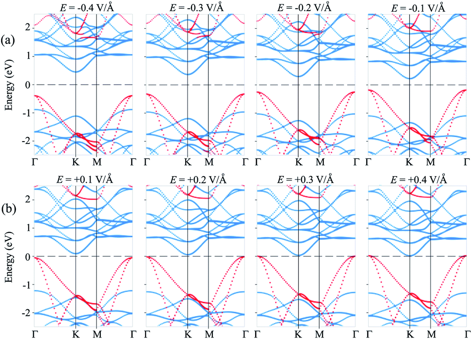 | ||
| Fig. 5 Projected band structures of the MoS2/SiH HTS under different values of (a) negative and (b) positive E. The contributions of the MoS2 and SiH layers are marked by blue and red circles, respectively. | ||
4 Conclusions
In conclusion, we have designed a type-II MoS2/SiH HTS and investigated its structural and electronic properties and the formation of the contact types by performing first principles calculations. The MoS2/SiH HTS is proved to be structurally and mechanically stable in the equilibrium state. The formation of the MoS2/SiH HTS leads to a reduction of the band gap compared to that of the constituent MoS2 and SiH monolayers, indicating that the electrons move quickly from the VB to the CB in such a HTS. Moreover, the MoS2/SiH HTS forms type-II band alignment, indicating that such a HTS is a promising candidate as an efficient photoelectric device because the photogenerated carriers in type-II are separated in each material. Furthermore, the electronic properties and contact type of the MoS2/SiH HTS can be modulated by an external electric field. The application of a negative electric field leads to a transformation from type-II to type-I band alignment. While the application of a positive electric field gives rise to a transition from semiconductor to metal in the MoS2/SiH HTS. These results could provide useful information for the design and synthesis of photoelectric devices based on the MoS2/SiH HTS.Conflicts of interest
There are no conflicts to declare.Acknowledgements
This research was funded by the University of Danang – University of Science and Technology, under project number T2021-02-10.References
- K. S. Novoselov, A. K. Geim, S. V. Morozov, D.-e. Jiang, Y. Zhang, S. V. Dubonos, I. V. Grigorieva and A. A. Firsov, Science, 2004, 306, 666–669 CrossRef CAS PubMed.
- P. Miró, M. Audiffred and T. Heine, Chem. Soc. Rev., 2014, 43, 6537–6554 RSC.
- S. Z. Butler, S. M. Hollen, L. Cao, Y. Cui, J. A. Gupta, H. R. Gutiérrez, T. F. Heinz, S. S. Hong, J. Huang and A. F. Ismach, et al., ACS Nano, 2013, 7, 2898–2926 CrossRef CAS PubMed.
- D. Akinwande, C. Huyghebaert, C.-H. Wang, M. I. Serna, S. Goossens, L.-J. Li, H.-S. P. Wong and F. H. Koppens, Nature, 2019, 573, 507–518 CrossRef CAS PubMed.
- M. Chhowalla, D. Jena and H. Zhang, Nat. Rev. Mater., 2016, 1, 1–15 Search PubMed.
- L. Peng, Y. Zhu, D. Chen, R. S. Ruoff and G. Yu, Adv. Energy Mater., 2016, 6, 1600025 CrossRef.
- Z. Guo, J. Zhou, L. Zhu and Z. Sun, J. Mater. Chem. A, 2016, 4, 11446–11452 RSC.
- L. Zhang, K. Khan, J. Zou, H. Zhang and Y. Li, Adv. Mater. Interfaces, 2019, 6, 1901329 CrossRef.
- C. R. Dean, A. F. Young, I. Meric, C. Lee, L. Wang, S. Sorgenfrei, K. Watanabe, T. Taniguchi, P. Kim and K. L. Shepard, et al., Nat. Nanotechnol., 2010, 5, 722–726 CrossRef CAS PubMed.
- K. Y. Ma, L. Zhang, S. Jin, Y. Wang, S. I. Yoon, H. Hwang, J. Oh, D. S. Jeong, M. Wang and S. Chatterjee, et al., Nature, 2022, 606, 88–93 CrossRef CAS PubMed.
- M. Z. Rahman, C. W. Kwong, K. Davey and S. Z. Qiao, Energy Environ. Sci., 2016, 9, 709–728 RSC.
- A. Carvalho, M. Wang, X. Zhu, A. S. Rodin, H. Su and A. H. Castro Neto, Nat. Rev. Mater., 2016, 1, 1–16 Search PubMed.
- A. C. Neto, F. Guinea, N. M. Peres, K. S. Novoselov and A. K. Geim, Rev. Mod. Phys., 2009, 81, 109 CrossRef.
- M. S. Jang, H. Kim, Y.-W. Son, H. A. Atwater and W. A. Goddard III, Proc. Natl. Acad. Sci. U. S. A., 2013, 110, 8786–8789 CrossRef CAS PubMed.
- M. Akhtar, G. Anderson, R. Zhao, A. Alruqi, J. E. Mroczkowska, G. Sumanasekera and J. B. Jasinski, npj 2D Mater. Appl., 2017, 1, 1–13 CrossRef.
- A. K. Geim and I. V. Grigorieva, Nature, 2013, 499, 419–425 CrossRef CAS PubMed.
- K. Novoselov, A. Mishchenko, A. Carvalho and A. Castro Neto, Science, 2016, 353, aac9439 CrossRef CAS PubMed.
- S. Wang, J.-P. Chou, C. Ren, H. Tian, J. Yu, C. Sun, Y. Xu and M. Sun, Sci. Rep., 2019, 9, 1–7 CrossRef PubMed.
- X. Gao, Y. Shen, Y. Ma, S. Wu and Z. Zhou, Carbon, 2019, 146, 337–347 CrossRef CAS.
- H. Henck, Z. B. Aziza, D. Pierucci, F. Laourine, F. Reale, P. Palczynski, J. Chaste, M. G. Silly, F. Bertran and P. Le Fevre, et al., Phys. Rev. B, 2018, 97, 155421 CrossRef CAS.
- P. Solís-Fernández, M. Bissett and H. Ago, Chem. Soc. Rev., 2017, 46, 4572–4613 RSC.
- R. Dong and I. Kuljanishvili, J. Vac. Sci. Technol., B: Nanotechnol. Microelectron.: Mater., Process., Meas., Phenom., 2017, 35, 030803 Search PubMed.
- W. Wei, Y. Dai, Q. Sun, N. Yin, S. Han, B. Huang and T. Jacob, Phys. Chem. Chem. Phys., 2015, 17, 29380–29386 RSC.
- Y. Luo, S. Wang, K. Ren, J.-P. Chou, J. Yu, Z. Sun and M. Sun, Phys. Chem. Chem. Phys., 2019, 21, 1791–1796 RSC.
- J. Su, L. Feng and Z. Liu, RSC Adv., 2016, 6, 59633–59638 RSC.
- B. Zeng, Y. Dong, Y. Yi, D. Li, S. Zhang and M. Long, J. Phys.: Condens. Matter, 2019, 31, 165502 CrossRef CAS PubMed.
- O. D. Restrepo, R. Mishra, J. E. Goldberger and W. Windl, J. Appl. Phys., 2014, 115, 033711 CrossRef.
- A. F. Wani, B. Rani, S. Dhiman, U. B. Sharopov and K. Kaur, Int. J. Energy Res., 2022, 46, 10885–10893 CrossRef CAS.
- J. Zeng, L. Xu, X. Luo, B. Peng, Z. Ma, L.-L. Wang, Y. Yang and C. Shuai, Phys. Chem. Chem. Phys., 2021, 23, 2812–2818 RSC.
- D. Fang, Y. Zhang and S. Zhang, New J. Phys., 2014, 16, 115006 CrossRef.
- S. Han, Y. Li, J. Chai and Z. Wang, Phys. Chem. Chem. Phys., 2020, 22, 8565–8571 RSC.
- K. F. Mak, C. Lee, J. Hone, J. Shan and T. F. Heinz, Phys. Rev. Lett., 2010, 105, 136805 CrossRef PubMed.
- Z. Ben Aziza, H. Henck, D. Pierucci, M. G. Silly, E. Lhuillier, G. Patriarche, F. Sirotti, M. Eddrief and A. Ouerghi, ACS Nano, 2016, 10, 9679–9686 CrossRef CAS PubMed.
- H. Henck, Z. B. Aziza, O. Zill, D. Pierucci, C. H. Naylor, M. G. Silly, N. Gogneau, F. Oehler, S. Collin and J. Brault, et al., Phys. Rev. B, 2017, 96, 115312 CrossRef.
- E. Lee, S. G. Lee, W. H. Lee, H. C. Lee, N. N. Nguyen, M. S. Yoo and K. Cho, Chem. Mater., 2020, 32, 4544–4552 CrossRef CAS.
- Z. Cui, K. Ren, Y. Zhao, X. Wang, H. Shu, J. Yu, W. Tang and M. Sun, Appl. Surf. Sci., 2019, 492, 513–519 CrossRef CAS.
- Q. Fu, X. Wang, J. Zhou, J. Xia, Q. Zeng, D. Lv, C. Zhu, X. Wang, Y. Shen and X. Li, et al., Chem. Mater., 2018, 30, 4001–4007 CrossRef CAS.
- P. Hohenberg and W. Kohn, Phys. Rev., 1964, 136, B864 CrossRef.
- G. Kresse and J. Furthmüller, Phys. Rev. B: Condens. Matter Mater. Phys., 1996, 54, 11169 CrossRef CAS PubMed.
- G. Kresse and J. Hafner, Phys. Rev. B: Condens. Matter Mater. Phys., 1993, 47, 558 CrossRef CAS PubMed.
- J. P. Perdew, K. Burke and M. Ernzerhof, Phys. Rev. Lett., 1996, 77, 3865 CrossRef CAS PubMed.
- G. Kresse and J. Furthmüller, Comput. Mater. Sci., 1996, 6, 15–50 CrossRef CAS.
- J. Heyd, J. E. Peralta, G. E. Scuseria and R. L. Martin, J. Chem. Phys., 2005, 123, 174101 CrossRef PubMed.
- S. Grimme, J. Comput. Chem., 2006, 27, 1787–1799 CrossRef CAS PubMed.
- C. Ataca, H. Sahin, E. Akturk and S. Ciraci, J. Phys. Chem. C, 2011, 115, 3934–3941 CrossRef CAS.
- W. Sheng, Y. Xu, M. Liu, G. Nie, J. Wang and S. Gong, Phys. Chem. Chem. Phys., 2020, 22, 21436–21444 RSC.
- S. Han, Y. Li and Z. Wang, Phys. Chem. Chem. Phys., 2020, 22, 17145–17151 RSC.
- H. Jin, Y. Dai, X.-C. Ma, L. Yu, W. Wei and B.-B. Huang, RSC Adv., 2015, 5, 52264–52268 RSC.
- S. Han, Y. Li and Z. Wang, Phys. E., 2021, 134, 114869 CrossRef CAS.
- F. Mouhat and F.-X. Coudert, Phys. Rev. B: Condens. Matter Mater. Phys., 2014, 90, 224104 CrossRef.
Footnote |
| † Electronic supplementary information (ESI) available. See https://doi.org/10.1039/d2ra03817j |
| This journal is © The Royal Society of Chemistry 2022 |