
 Open Access Article
 This Open Access Article is licensed under a Creative Commons Attribution-Non Commercial 3.0 Unported Licence
Label-free plasmonic-based biosensing using a gold nanohole array chip coated with a wafer-scale deposited WS2 monolayer†
Lixing Kang‡
 *abc,
Yan Zhang‡de,
Qian Gong‡c,
Chandreyee Manas Dasab,
Huilin Shaode,
Daniel Puiu Poenar*ab,
Philippe Coquetaf and
Ken-Tye Yongg
*abc,
Yan Zhang‡de,
Qian Gong‡c,
Chandreyee Manas Dasab,
Huilin Shaode,
Daniel Puiu Poenar*ab,
Philippe Coquetaf and
Ken-Tye Yongg
aCINTRA CNRS/NTU/THALES, UMI 3288, Research Techno Plaza, 50 Nanyang Drive, Border X Block, Singapore 637553, Singapore. E-mail: lxkang2013@sinano.ac.cn
bSchool of Electrical and Electronic Engineering, Nanyang Technological University, 50 Nanyang Avenue, Singapore 639798, Singapore. E-mail: EPDPuiu@ntu.edu.sg
cDivision of Advanced Materials, Suzhou Institute of Nano-Tech and Nano-Bionics, Chinese Academy of Sciences, Suzhou 215123, China
dInstitute for Health Innovation & Technology, National University of Singapore, Singapore 117583, Singapore
eDepartment of Biomedical Engineering, Faculty of Engineering, National University of Singapore, Singapore 117583, Singapore
fInstitut d’Electronique, de Microélectronique et de Nanotechnologie (IEMN), CNRS UMR 8520 – Université de Lille 1, Villeneuve d’Ascq 59650, France
gThe University of Sydney Nano Institute, The University of Sydney, Sydney 2006, New South Wales, Australia
First published on 21st November 2022
Abstract
This paper reports the fabrication, testing and obtained performance of a plasmonic sensor employing a gold (Au) nanohole array chip coated with tungsten disulphide (WS2), which is then functionalized for the detection of protein–protein interactions. A key novelty is that the WS2 was deposited as a monoatomic layer using a wafer-scale synthesis method that successfully provided a film of both high quality and uniform thickness. The deposited WS2 film was transferred onto a Au nanohole array chip using a novel method and was subsequently functionalized with biotin. The final sensor was tested and it demonstrated efficient real-time and label-free plasmonic detection of biotin–streptavidin coupling. Specifically, compared to a standard (i.e. uncoated) Au nanohole-based sensor, our WS2-coated Au nanohole array boosted the spectral shift of the resonance wavelength by ∼190%, resulting in a 7.64-fold improvement of the limit of detection (LOD).
1. Introduction
Plasmonic immunosensors have become increasingly popular and found numerous applications. Their underlying operating principle is the generation of a readable optical signal upon binding of either an antigen (AG) or antibody (Ab) onto a surface functionalized with its conjugate analyte.1 Since these sensors offer numerous benefits, such as high sensitivity and accuracy as well as rapid response time, they have been utilized in medical diagnostics and pathology.2–11 Surface Plasmon Resonance (SPR) is a physical phenomenon whereby the incident light wave interacts with a plasmonic metal (usually Au) of nanometer-range thickness and excites the free electrons at the surface of the metal (i.e. at its interface with the overlying dielectric, typically a liquid analyte which contains the (bio)molecule to be detected) into coherent oscillations, the so-called Surface Plasmon Polaritons (SPPs). Most SPR-based biosensors utilize the well-known Kretschmann configuration that consists of a gold (Au) thin film, about 50 nm thick, coated on top of a glass prism. When light is incident through the glass prism at a resonance, or critical angle (at which Total Internal Reflection (TIR) occurs) onto a metal–dielectric (usually Au–liquid) interface, SPPs are generated at this interface. They propagate and decay as an evanescent wave in the liquid, enabling to detect refractive index (RI) changes due to the presence of analyte molecules either in the bulk of the liquid sample (if no functionalization is present at the interface) or at the interface. In the latter case, the molecules to be detected are captured in a functionalization layer with high affinity only towards the targeted (bio)molecule, e.g. using an antigen–antibody type interaction, that is coated onto the sensor surface. The SPP-induced evanescent electromagnetic (EM) field diminishes exponentially away from the interface as the corresponding EM wave traverses through the analyte. The penetration depth of this field, Lp, usually defined as the distance from the metal–dielectric interface at which the value of the field is 1/e times the maximum value (where e is the base of the natural logarithm), is of the order of half the wavelength of the incident light.12–14 Biomolecular antigen–antibody interactions that capture the desired biomolecules within this penetration depth can bring forth a change in the response signal. Thus, even the slightest change in the RI of the analyte causes the SPR angle to shift. Hence, in the case of SPR immunosensors, the binding of an antigen (flowing through/present in the analyte) to an antibody a priori immobilized on the sensor surface results in a change in RI that shifts the SPR angle. In commercial SPR sensors, the shift in resonance angle is observed in a sensorgram and it is usually expressed in resonance units (RU). For most sensors, a change of 1000 RU corresponds to a change of about 0.1° in the SPR angle. The sensorgram can provide useful information about the antibody–antigen interaction, such as the affinity between the two interlocking molecules and their associated kinetics.15Recently, new plasmonic nanostructures have been proposed that can enhance the sensitivity, detection limits and accuracy of SPR-based biomolecular sensors. Chips employing nanohole arrays realized in Au films possess unique optical properties that have been utilized for the realization of a new kind of SPR sensors. For example, Xue et al. used antimonene-modified gold SPR chips to detect microRNA hybridization events.16 The nanohole-based sensing is based on the “extraordinary optical transmission” (EOT) phenomenon. Specifically, as was indicated previously in literature,17 Bethe developed the theory for the diffraction of light through small holes in a metal film,18 which was then first challenged and ultimately completed by the discovery of the EOT through arrays of subwavelength apertures.19 Quantitatively, the amount of light transmitted through a nano-aperture in an opaque metal decreases with decreasing the hole area, namely scaling with d/λ4, with d being the nanoaperture diameter and λ the incident light wavelength.18 Consequently, the overall transmission through a hole in an opaque metal film should be negligible if the size of the hole is smaller than the wavelength of the incident radiation. However, this was not what Ebbesen and his co-workers19 observed in 1998, when they performed light transmission experiments through nanohole arrays in Au and Ag films. Contrary to the then-popular Bethe's law, they observed that the transmitted light was enhanced at certain wavelengths. This unusual principle was called EOT and, indeed, Bethe's theory was subsequently extended to arrays of such nano-apertures.20–22 The EOT effect in nanoholes in a metal is due to the excitation of SPs that results in increased light transmittivity. In a typical nanohole sensing array, the EOT resonance condition is observed as a peak in the transmissivity versus wavelength curve and it can reach as much as 100% at resonant wavelengths,23,24 which is not a contradiction to Bethe's original work.16 The value of the specific resonance wavelength depends on the dielectric constants of the metal and of the adjacent medium.
In the case of SPR, bio-molecular interactions (e.g. capture via antigen–antibody interactions) that take place within the penetration depth Lp, which is usually on the order of about 200 nm, result in a shift of the resonance wavelength since the ligand–analyte coupling changes the RI of the dielectric analyte at the interface with the SPR sensor.25,26 Commercial SPR sensors that utilize the traditional Kretschmann configuration need a prism coupling system to match the propagation constant of the incident light with that of the surface plasmons (SPs), as this is a necessary and essential condition for exciting the SPPs. However, the patterning of the plasmonic metal in a metallic nanohole array structure can confine SPs at the metal–dielectric interface without the need of any additional optical instruments. Hence, a unique plasmonic excitation system can be realized even when using an inexpensive light-emitting diode (LED) and a camera. Consequently, unlike the traditional Kretschmann configuration for SPR sensors, a nanohole array chip-based SPR immunosensor does not require additional costly and bulky optical components and, therefore, is a highly desirable and suitable alternative to SPR for the development of next generation point-of-care (POC) clinical devices.27,28
Additionally, the use of two-dimensional (2D) materials in many optoelectronic applications and devices, such as photodetectors and optical modulators, has given promising results in terms of improved detection capabilities and higher sensitivity. This enhanced performance is due to the advantageous physical, chemical, optical and electrical properties of these materials. Recent work on 2D transitional metal dichalcogenides (TMDCs) has shown that their usage in conjunction with various biomolecules with intrinsic enzymatic capabilities, such as glucose, cholesterol, glutathione and cysteine, result in the so-called nanozymes. Nanozymes are a novel class of nanomaterials exhibiting enzyme-like properties and activities. They are a promising alternative to natural enzymes because their properties can be tailored for the desired purpose, and as such they show great promise for biosensing and therapeutic applications.29 Tungsten disulfide (WS2) is one of the desirable choices among the many TMDC materials discovered to this date. It has a high optical absorption coefficient of 105–106 cm−1 and a thickness-dependent bandgap of 1.3–2.05 eV.30–36 Because the atoms of TMDCs exhibit a strong in-plane covalent bonding and weak van der Waals's interlayer bonding, these layered 2D materials can be effectively prepared from their bulk counterparts. However, it is absolutely necessary to use high quality WS2 films that are both uniformly thick and crystalline in order to achieve high accuracy and efficiency of the optoelectronic devices using them. Therefore, in order to address these critical requirements that are typically very hard to be satisfactorily met simultaneously, we have developed a special WS2 synthesis approach for depositing films of very high quality even on very large areas. For this purpose, chemical vapor deposition (CVD) was employed to fabricate atomically thin WS2 monolayer films on very large areas, namely on the entire surface of a 2-inch wafer-scale SiO2/Si substrate. However, instead of a single-zone furnace we utilized a multi-zone furnace as it allows better control of different internal processes, such as evaporation and material deposition.37–40 Using a three-zone horizontal furnace, the evaporation and deposition temperatures in the three zones can be precisely controlled and this can facilitate the deposition of WS2 films of high crystalline quality and of uniform thickness even over the large areas mentioned previously. Apart from these much desired characteristics, the deposited WS2 films were also extremely flexible. When such films were used in large-area photodetectors, enhanced photoresponsivity along with faster response times were observed.40
We have used the same multi-zone CVD approach to deposit monolayer WS2 films that were subsequently employed in our Au nanohole array chip-based plasmonic sensors. Besides the original wafer-scale CVD method mentioned earlier, another novelty of our sensor design lies in the transfer of the WS2 monolayer on top of a Au nanohole array chip. As a result, the optical transmission of the metallic nanohole array chip was further enhanced due to the addition of this WS2 thin film. Furthermore, when this structure was used to study the interaction between biotin and streptavidin, it was observed that the addition of the WS2 to the Au nanohole array chip also increased significantly the shift of the latter's resonant wavelength. Consequently, our WS2-covered Au nanohole array chip plasmonic sensor exhibited increased sensitivity towards bio-molecular interactions as compared to a standard Au nanohole array chip sensor which does not have any additional coating. Section 2 will present the fabrication details of the Au nanohole array chip and WS2 films. Section 3 will detail the various material characterization results along with a detailed interpretation of the biotin–streptavidin coupling results measured with our fabricated Au nanohole array chip-WS2 plasmonic sensor. We end this paper with a concluding note in Section 4.
2. Materials and methods
2.1 Fabrication of gold nanohole array chip
Nanohole array chips were fabricated on 2.5 × 2.5 cm2 glass/Indium Tin Oxide (ITO) substrates. The ITO layer is critical to improve the conductivity of the substrate for the subsequent steps. First, the substrate was spin-coated with 180 nm of 10% wt polymethyl methacrylate (PMMA, Aladdin) 495K photoresist, followed by hard baking on a hotplate at 170 °C for 5 min. Next, a second layer of PMMA 495K of the same thickness was spin-coated on the substrate, followed by post-bake at 180 °C for 2 min. After the spin-coating of the two successive layers of PMMA photoresist, electron-beam lithography (EBL) was performed to define the nanohole array chip pattern in the photoresist according to our previously reported method.25 The exposure was followed by development of the photoresist in an organic solvent mixture of methyl isobutyl ketone (MIBK, Alfa, ≥99.5%) and Isopropyl Alcohol (IPA) in a ratio of 1![[thin space (1/6-em)]](https://www.rsc.org/images/entities/char_2009.gif) :3 for 45 s. After developing, Ti/Au (10 nm/100 nm) thin films were deposited onto the substrate using electron beam physical vapor deposition, followed by lift-off in solvent stripper. All nanohole dimensions and sensor uniformity were then characterized by scanning electron microscopy (SEM, S-4800, HITACHI, Japan).
:3 for 45 s. After developing, Ti/Au (10 nm/100 nm) thin films were deposited onto the substrate using electron beam physical vapor deposition, followed by lift-off in solvent stripper. All nanohole dimensions and sensor uniformity were then characterized by scanning electron microscopy (SEM, S-4800, HITACHI, Japan).
2.2 Fabrication of monolayer WS2 films
A horizontal furnace and a quartz tube (3 inch in diameter) were employed for the wafer-scale synthesis of monolayer WS2 films. For this purpose, the precursor materials, namely sulfur (300 mg) and WCl6 (30 mg) powders, were placed in separate quartz boats located upstream of the gas flow, as illustrated in Fig. 1. Single-side polished Si wafers 2 inch in diameter, a priori covered with a SiO2 film 300 nm thick, were purchased from Silicon Valley Microelectronics, Inc. The SiO2/Si wafers were used as the WS2 deposition substrates located downstream in the furnace. The precursor materials react at elevated temperatures to produce WS2, which may subsequently precipitate onto the receiving substrates to yield WS2 films. The deposition temperature was fixed at 900 °C. Before heating, the base pressure of the tube was pumped down to 1 mTorr. Argon (300 sccm) and hydrogen (20 sccm) were introduced in the system during the material deposition. The deposition time was 30 min. After the WS2 deposition, the system was cooled naturally to room temperature under Ar flow.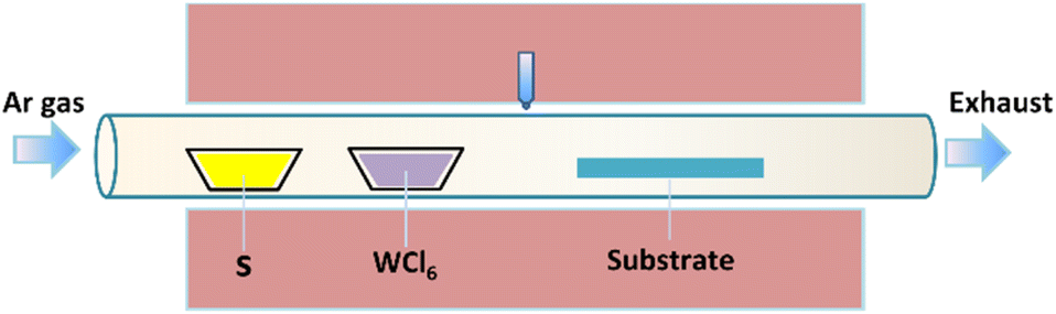 | ||
| Fig. 1 Schematic illustration of the experimental CVD setup used for wafer-scale WS2 deposition in a horizontal furnace. | ||
2.3 Transferring the WS2 film onto the gold nanohole array chip
A thin PMMA film was spin-coated (3000 rpm, 1 min) on top of the WS2 layer deposited onto the SiO2/Si substrate and cured at 120 °C for 2 min. The PMMA/WS2 film was detached from the substrate by etching the SiO2 layer in 2% wt hydrogen fluoride solution (obtained by dilution with DI water of HF with concentration ≥40% purchased from Alfa), as shown in Fig. S1 in the ESI file.† After rinsing in deionized (DI) water, the PMMA/WS2 film was floated on the water, which could be scooped up by, and attached onto, the Au nanohole array chip and dried on a hot plate (80 °C). Finally, the PMMA was removed by rinsing with toluene several times. The residual WS2 film was tightly adsorbed on the surface of the Au nanohole array chip.2.4 Functionalization of the WS2 film
The process steps for the functionalization of the WS2 film surface are shown in Fig. S2 in the ESI file.† The sensor fabricated as described in the previous section was first carefully rinsed with DI water and dried under a stream of nitrogen gas. All the surface functionalization was done by dropping 10 μL of corresponding solution on each sensing site and incubating in a humid chamber at room temperature (25 °C), atmospheric pressure and 95% relative humidity for 2 hours. The use of polyethylene glycol (PEG, Aladdin, ≥99%) as linker was important in order to minimize the non-specific target binding and improve surface hydrophilicity. A previous study showed that a 1:3 mixture of long and short PEGs exhibited the best capture yield,28 which could thus enhance the detection sensitivity of our sensor. The sulfhydryl (HS) group reacts readily with many thiol reactive groups, and can also easily bind to Au and other noble metal surfaces with high affinity. The realized conjugated sensors were stored in phosphate buffered saline solution (PBS, 0.1 M, pH 7.0) at 4 °C for subsequent use. All sensor surface modifications were spectrally monitored to ensure uniform functionalization, as described in Section 2.6. The morphology of the functionalized WS2 films was characterized by transmission electron microscopy (TEM, TecnaiG2 F20 S-TWIN, FEI, USA), and the obtained images are shown in Fig. S6 in the ESI file.† The photos in that Figure show clearly the ordered structure of the WS2 surface after functionalization, whereby the few white spots in Fig. S6a† are due to proteins that remained attached onto the surface.
2.5 Biotin–streptavidin coupling
For this study, biotin–streptavidin coupling was chosen to demonstrate the sensor's capability for highly sensitive biological detection. The choice of biotin–streptavidin coupling was due to the fact that this AG–Ab pair has been widely used for SPR immunoassays, especially in sandwich-based signal enhancement assays. This system is also simple and very effective because of its high binding capacity, reproducibility and chemical resistance.Specifically, we functionalized both the bare and the WS2-coated Au nanohole array chips with thiol-PEG biotin as described previously in Section 2.4, and then employed polystyrene (PS) beads coated with 70 nm of streptavidin as detection targets, as illustrated in Fig. S3 in the ESI file† and 7a. After the thiol-PEG functionalization, the sensors chips were washed with PBS three times consecutively and blown dried with nitrogen, after which a suspension solution of streptavidin-coated PS beads was applied onto the biotin-functionalized sensor surface as was also indicated in Section 2.4, and incubated for 30 min. After target incubation, the sensor surface was first washed with PBS for 5–10 min. This was immediately followed by another set of measurements with another suspension of PS beads with a different concentration. The previously captured beads were not removed as the new measurements with different concentration of beads were subsequently performed at different sensor sites or with a different new fresh sensor. The process was then repeated as many times as necessary, until the behaviour for all concentrations of interest has been fully characterized.
2.6 Optical and spectrometric analyses
A tungsten halogen lamp (4.75 W, StockerYale Inc.) was used to back-illuminate the Au nanohole array chip sensor (with or without WS2 layer) through a ×10 microscope objective. The transmitted light was collected by an optical fiber and fed into a spectrometer (Ocean Optics Flame spectrometer), which analyzed the transmitted light in the wavelength range 336 nm to 1661 nm, with a step of 0.4 nm. The main goal was to determine the performance of the sensors, i.e. to investigate the spectral behaviour of the Au nanohole array chips (with or without WS2 layer) for different RI values of the analyte. For this purpose, a series of sucrose solutions with different concentrations were used. The RI of each solution was determined with a uniREFRACTO digital handheld refractometer before measurement and the RI values were in the range between 1.333 and 1.362. All measurements were performed at room temperature, in an enclosed box to eliminate ambient light interference. The transmitted light intensity was digitally recorded in counts against wavelength by the Ocean optics flame spectrometer and processed using Oceanview 1.6.5 software. For spectral analysis, the spectral peaks were determined using a custom-built R program by fitting each transmission peak with a multi-order polynomial curve using the local regression method.In order to quantify the limit of detection (LOD) of the Au nanohole array chip sensors without and with WS2 top coating, additional spectral measurements were performed. The baseline spectrum of the functionalized sensors was first measured in PBS buffer before introducing the beads suspension onto the sensor. A minimum value of 0.25 nm was determined for the shift of the main transmission peak detection level using three times the value of the standard deviation of the spectral peak position measured in PBS in steady state for 5 min. The LOD of each sensor was then extracted by determining the intersection point between the measured titration curve and this minimum level, and the results are indicated in subsequent Section 3.3.
3. Results and discussion
3.1 Morphological and structural characterization of deposited WS2 films
We have successfully deposited monolayer WS2 films on 2-inch SiO2/Si substrates, as shown in Fig. 2. It can be easily seen that the deposited WS2 thin film is continuous and uniform over the entire wafer surface area.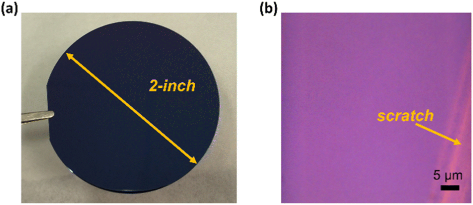 | ||
| Fig. 2 Monolayer WS2 films grown on SiO2/Si substrates. (a) Photo of a 2 inch wafer covered with a WS2 monolayer; (b) microscope image of the WS2 monolayer with an intentional scratch. | ||
A key advantage of the method described in Section 2.2 is that the number of atomic layers in the deposited WS2 films can be very precisely controlled by controlling the amount of WCl6 used in experiments. Further characterizations were performed to investigate the composition and structure of the as-deposited WS2 films and to confirm that it is indeed only one atomic layer thick and of good crystalline quality. The atomic force microscopy (AFM) images in Fig. 3a and b show that the thickness of the synthesized WS2 monolayer in that examined sample was 0.64 nm. Thickness characterization measurements were performed on ten WS2 monolayer samples, whose measured thickness ranged between 0.6 and 0.9 nm, as shown in Table ST1 in the ESI file.† Likewise, the Raman shifts have also been measured for the same WS2 monolayer samples, as shown in Table ST2 in the ESI file.† The mean value of the WS2 monolayer thickness and its standard deviation resulted from all these data are 0.723 nm, and 0.097 nm, respectively. The mean value of the Raman shift for the E12g peak and its standard deviation are 356.385 cm−1, and 0.9899 cm−1, respectively. Fig. 3c shows the Raman spectrum of the obtained WS2 films, which exhibits 2 characteristic Raman modes, A1g and E12g. The full width at half maximum (FWHM) of the E12g peak is 4.3 cm−1, close to that of the exfoliated monolayer, 3.7 cm−1. This suggests a very good crystalline quality in the synthesized film. Furthermore, the photoluminescence (PL) spectrum illustrated in Fig. 3d shows a very sharp and strong single peak at ∼625 nm, which suggests that the deposited WS2 film is a monolayer with a band gap of ∼2 eV.
 | ||
| Fig. 3 Structural characterization of our monolayer WS2 film: (a) AFM scan image taken over the transition from a region without deposited WS2 film (left side), to one with deposited film (right side). (b) Height profile along the white dashed line shown in (a). (c) Raman spectrum of the WS2 monolayer film grown on silicon substrates. (d) Photoluminescence (PL) of the synthesized WS2. | ||
After the transfer of the synthesized WS2 film onto the Au nanohole array chip (Fig. 4a and b), obvious differences can be noticed in Fig. 4c between WS2-covered and bare Au nanohole arrays.
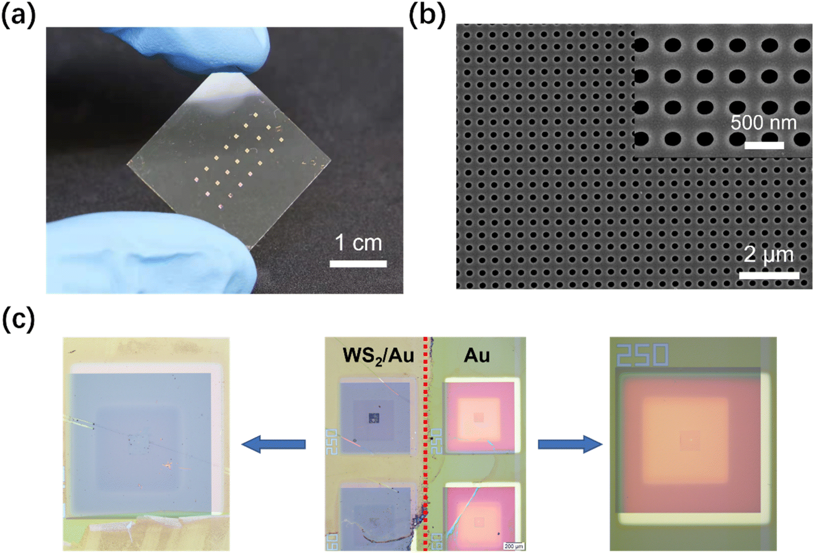 | ||
| Fig. 4 Images of our sensors with Au nanohole arrays. (a) A photograph of the final WS2-coated Au nanohole microarray sensor. (b) SEM image of a portion of the initial bare Au nanohole microarray. (c) The final WS2–Au nanohole sensor after the transfer of WS2 film onto the Au nanohole array chip (left side), compared to the bare (non-WS2-coated) Au nanohole array chip (right side). | ||
3.2 Optical performance of the sensors
Fig. 5 shows the performance of the bare Au nanohole array chip (i.e. without any WS2 film added onto it) when subjected to analytes of various RI values. It can be seen in Fig. 5a that there are three important and useful peaks in the transmission spectrum. The first is a smaller but very clearly defined peak situated in the range 630–640 nm, followed by two other peaks, one in the range 620–640 nm, and the other in the range 700 to 720 nm, respectively. However, although these two other peaks have much larger amplitudes, they also are broader and have more bandwidth fluctuations than the first peak. Thus, the second and third peak are not suitable to measure small changes in the surrounding analyte's RI value. Fig. 5b shows similar plots, but for the Au nanohole array chip with the WS2 film added onto it.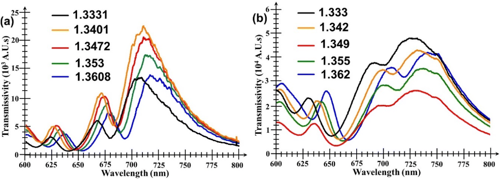 | ||
| Fig. 5 Transmission spectra of: (a) bare Au nanohole array without any WS2 film, and (b) the chip covered with WS2 film. In both cases the sensors were exposed to solutions of sucrose with different RI values indicated in each case. | ||
The plot in Fig. 6a compares the transmissions of both the bare Au nanoarray sensor and the WS2-coated one when PBS was used as analyte. It is evident that the addition of the WS2 film atop the Au nanoarray had a beneficial influence by increasing the magnitude of all the 3 initial transmission peaks of the bare Au sensor. The generally increased transmissivity of the WS2-coated Au nanohole array chip is due to enhanced generation of SPs induced by the additional TMDC layer. However, at the same time, it can also be seen that, for the WS2-coated sensor, the central wavelengths of all peaks exhibit a visible red shift towards larger wavelengths caused by the addition of the WS2 film atop the Au nanohole array chip. The peak wavelength of the first peak is red-shifted with 5.6 nm, but the most significant changes/red-shifts are especially those of the second peaks with values of 26.89 nm. Unfortunately, the second and third peaks have now almost merged because of the largest red-shift exhibited by the second peak as well as the significant broadening of both these peaks. This would make much more difficult their detection and extraction of the exact amount of their wavelength shift, further supporting our previous statement that the second and third peaks are much less suitable for an accurate quantitative analysis that would provide the desired information about the analyte's RI value.
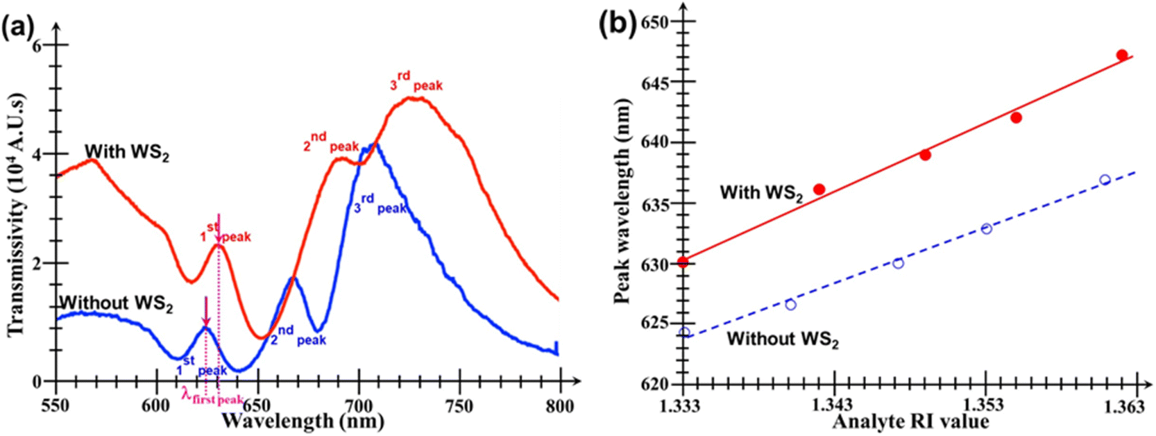 | ||
| Fig. 6 (a) Transmitted light spectra of bare Au nanohole array with and without the added WS2 film, when exposed to PBS. (b) Dependence of the first transmission peaks' wavelengths as a function of the solution's RI value for the Au nanohole sensors without and with WS2 film, respectively. | ||
The recognition mechanism for the analyte is based on biotin–streptavidin interaction. We first modified the sensor surface with biotin-PEG linkers and used streptavidin-coated PS beads (purchased from Spherotech) as analyte. The interaction of biotin and streptavidin has been exploited in many protein and nucleic acid detection and purification methods. Streptavidin is a 66 kDa (tetramer) protein purified from the bacterium Streptomyces avidinii. Streptavidin homo-tetramers have an extraordinarily high affinity for biotin (also known as vitamin B7 or vitamin H). With a dissociation constant (Kd) on the order of about 10−14 mol L−1, the binding of biotin to streptavidin is one of the strongest non-covalent interactions known in nature. Streptavidin is used extensively in molecular biology and bionanotechnology due to the streptavidin–biotin complex's resistance to organic solvents, denaturants (e.g. guanidinium chloride), detergents (e.g. SDS, Triton X-100), proteolytic enzymes, and extremes of temperature and pH.
Fig. 6b summarizes the linear dependencies of the central wavelengths of the first transmission peaks on the analyte's RI value for both types of chips. The key data extracted from the linear fitting equations for the red shift of the main transmission peaks of both types of sensors are summarized in Table 1. Fig. 5 and 6, as well as the data given in Table 1, show that the spectral shifts of both sensors present excellent linear correlation with increasing the analyte's RI value.
| Fitting parameter values | Bare Au nanohole array chip | WS2-covered Au nanohole array chip |
|---|---|---|
| Slope (sensitivity) m [nm/RIU] | 458.2 | 563.2 |
| Y-axis intercept n [nm] | 624.2 | 629.9 |
| R2 | 0.9934 | 0.9908 |
The data in Table 1 indicate that the sensitivity of the WS2-coated sensor was 1.23× larger than that of the bare Au nanohole array chip. Even if the shift of the second transmission peak were monitored to deduce the analyte's RI value, then the Au/WS2 sensor would still be approximately 22% more sensitive than the bare Au one. All these results prove that the addition of the WS2 film indeed increases the sensitivity of the Au nanohole array chip sensor.
3.3 Analysis of biotin–streptavidin biomolecular interactions
As mentioned in sub-sections 2.5 and 2.6, the performance of both sensors was assessed by subjecting them to suspensions of streptavidin-coated PS beads with different concentrations. The surface of our WS2–Au nanohole array chip immunosensor resulting after functionalization with biotin and tested using streptavidin-coated PS beads is schematically represented in Fig. 7a. All the measurements were performed in triplicate. Successive 1 μL suspensions of PS beads of different concentrations obtained by serial dilutions were applied to the sensor and incubated for 30 min. to complete the binding process. Unbound beads were washed away with PBS for three times before spectral measurements. The number of beads was determined using a Countess 3 automated cell counter. The titration curve was linearly fitted for subsequent analysis to extract both the corresponding slope (sensitivity) and the intersection between the fit line and the pre-determined minimum detection level necessary to determine the LOD value for each sensor, as was described at the end of previous Section 2.6.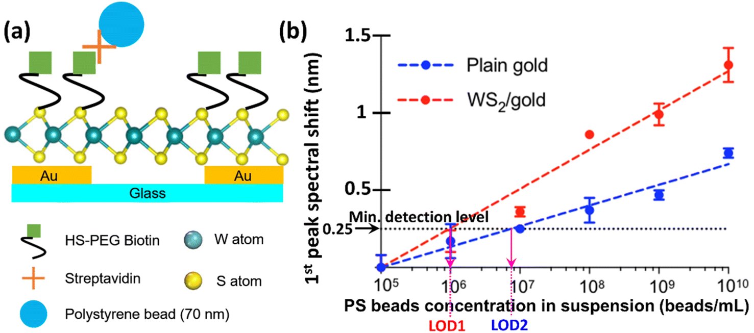 | ||
| Fig. 7 (a) Schematic representation of our WS2–Au nanohole array SPR immunosensor functionalized with biotin and tested using streptavidin-coated PS beads. (b) Measured optical spectral shift for the central wavelength of the first transmission peak as a function of the streptavidin-coated PS beads concentration for plain and WS2-coated Au nanohole arrays sensors functionalized with biotin. | ||
Because the RI value of the PS beads (1.59) is higher than that of the surrounding PBS solution (1.334), the sensors will exhibit a shift of the first transmission peak proportional to the number of bounded PS beads on surface. Indeed, as expected from the previous measurements with analyte solutions of different RI values, in this case, too, the RI of the analyte changed as the number of beads increased, resulting in a proportionally larger shift of the first transmission peak, as shown in Fig. 7b. The equations of the fitting lines and exact values of their extracted parameters are summarized in Table 2.
logx + n quantifying the measured dependence of the optical spectral shift for the first transmission peak as a function of the concentration of streptavidin-coated PS beads for plain and WS2-coated based Au nanohole arrays sensors functionalized with biotin
| Fitting parameter values | Bare Au nanohole array chip | WS2-covered Au nanohole array chip |
|---|---|---|
| Slope (sensitivity) m [nm logmL−1] |
0.1338 | 0.2542 |
| Y-axis intercept n [nm] | 0.2676 | 0.5084 |
| R2 | 0.964 | 0.969 |
| LOD [nr. of PS beads per mL] | 7.46 × 10⁶ | 106 |
Since the previous results determined that the central wavelengths of all the peaks in the transmission spectrum of the Au nanohole array chip sensors shifted when varying the RI of the analyte, a spectral shift in the first peak's central wavelength proportional to the beads concentration should occur in this case as well. Indeed, our measurements confirmed this fact. As it can be seen in Fig. 7a and b much more accentuated spectral shift for the first transmission peak can be noticed for the Au/WS2 sensor as compared to that of the bare Au nanohole array chip. The amplification, defined as the ratio between the spectral shifts for the Au/WS2 plasmonic nanosensor relative to that of the bare one, has a maximum value of 225% (0.4 nm wavelength shift for the bare Au and 0.9 nm for the WS2-coated Au nanoarray sensors) for a concentration of 108 PS beads per mL. The significantly improved performance of the WS2-coated sensor is also clear from the extracted values of both the slope of the fitting lines and the LOD values. It can be seen that the sensitivity of the Au/WS2 nanohole array sensor chip is almost twice as large as that for the plain Au sensor. This increased spectral shift sensitivity of the Au/WS2 sensor is due to the enhanced light–matter coupling at the nanoholes that produces more surface plasmons, thus resulting in an augmented transmittivity.
Finally, the WS2-coated sensor also is significantly more sensitive, exhibiting a LOD 7.46× smaller than that of the bare Au nanohole array chip sensor. This is because the LOD values expressed in terms of beads concentration for the WS2-coated nanohole array chip and the bare Au one are 106 PS beads per mL and 7.46 × 10⁶ PS beads per mL, respectively. However, because we only used 1 μL of solution for each measurement, the LOD can be expressed simply by the number of captured beads for this analyte volume, resulting in the corresponding values of 106 PS beads per mL and 7.46 × 10⁶ PS beads per mL, respectively. To compare these performances with the typical responses of other SPR biosensors, Table ST2 in the ESI file† compares LOD values reported in literature41–44 for different plasmonic sensors functionalized with different receptors for specific detection of various substances with RI and size similar to those of the PS beads (75 nm in diameter and RI = 1.59) used in this work. We also measured the SPR transmission intensity, full width at half maximum (FWHM) of the spectral peak, and detection sensitivity of different sensors. The obtained results show uniform fabrication and consistent optical performance across sensors (Table ST3†).
In fact, as is well known, most plasmon-based applications mainly rely on local field enhancement induced by metallic nanostructures at optical wavelengths for various applications, including biosensing.45–47 In other words, the observed improved performance of the sensor could be due to the manifestation of the same EOT phenomenon mentioned previously. In turn, this EOT appears because of the intense field concentration, inside and in the immediate vicinity of the Au nanoapertures, that provides a high transmission efficiency above unity.48
4. Conclusions
A Au nanohole array chip-based SPR sensing technology eliminates the need of having complex and bulky system components and thus it can be easily miniaturized and used in many lab-on-chip sensing applications. In this paper, we have designed a novel plasmonic sensor chip made up of a WS2 monolayer coated on top of an Au nanohole array chip substrate. The WS2 film has been deposited using an original CVD method that allows to obtain films of excellent crystalline quality and uniformity even on large area substrates. Specifically, our WS2-coated nano-plasmonic sensor detected biotin–streptavidin coupling with a 190% enhancement in sensitivity and a LOD 7.46 times smaller as compared to those of a simple Au nanohole array chip-based sensor when the wavelength shift of the first transmission peak is monitored. This observed shift of the plasmonic-enhanced transmission mainly depends on the properties of the metal film and the RI of the media on either side of the metal film. Particle binding increases the RI on the sensor surface, which induces a spectral shift to a longer wavelength.25,28 At the same time, we believe that the explanation for our device's significantly improved performance is that the addition of WS2 on top of the Au nanohole array chip promoted greater interaction between the incident light and the plasmonic substrate. This enhances the generation of surface plasmons with strong localized electric fields which, in turn, enhances the interaction between the sensor and the biocomponent, resulting in improved sensitivity and reduced LOD.Conflicts of interest
The authors declare that they have no known competing financial interests or personal relationships that influenced the work reported in this paper.Acknowledgements
This work was supported by the Singapore National Research Foundation (NRF) and French National Research Agency (ANR), grant number (NRF2017–ANR002 2DPS). The authors are grateful for the technical support for Nano-X from Suzhou Institute of Nano-Tech and Nano-Bionics, Chinese Academy of Sciences (SINANO).Notes and references
- D. R. Shankaran and N. Miura, J. Phys. D: Appl. Phys., 2007, 40, 7187–7200 CrossRef.
- L. K. Chin, T. Son, J.-S. Hong, A.-Q. Liu, J. Skog, C. M. Castro, R. Weissleder, H. Lee and H. Im, Acs Nano, 2020, 14, 14528–14548 CrossRef.
- K. V. Gobi, H. iwasaka and N. Miura, Biosens. Bioelectron., 2007, 22, 1382–1389 CrossRef PubMed.
- D. Conteduca, I. Barth, G. Pitruzzello, C. P. Reardon, E. R. Martins and T. F. Krauss, Nat. Commun., 2021, 12, 1–9 CrossRef PubMed.
- S. Qian, Y. Zhang, H. Yuan, W. Ji, Y. Liu, J. Zhao, M. Han and W. Peng, Sens. Actuators, B, 2018, 260, 76–982 Search PubMed.
- N.-F. Chiu, T.-Y. Huang, H.-C. Lai and K.-C. Liu, Nanoscale Res. Lett., 2014, 9, 445 CrossRef PubMed.
- S.-H. Oh, H. Altug, X. Jin, T. Low, S. J. Koester, A. P. Ivanov, J. B. Edel, P. Avouris and M. S. Strano, Nat. Commun., 2021, 12, 1–18 CrossRef PubMed.
- M. Pawula, Z. Altintas and I. E. Tothill, Talanta, 2016, 146, 823–830 CrossRef CAS.
- S. Firdous, S. Anwar and R. Rafya, Laser Phys. Lett., 2018, 15, 065602 CrossRef.
- A. R. Sadrolhosseini, S. A. Rashid, H. Soleimani, S. Shafie, A. S. M. Noor and A. Mohammadi, J. Phys.: Conf. Ser., 2018, 1123, 012016 CrossRef.
- Y. Nonobe, T. Yokoyama, Y. kamikubo, S. Yoshida, N. Hisajima, H. Shinohara, Y. Shiraishi, T. Sakurai and T. Tabata, BMC Biotechnol., 2016, 16, 36 CrossRef PubMed.
- J. Homola, S. S. Yee and D. Myszka, Optical Biosensors: Today and Tomorrow, Elseiver B.V., 2nd edn, 2008 Search PubMed.
- A. J. Tudos and R. B. M. Schasfoort, Handbook of Surface Plasmon Resonance, Royal Society of Chemistry, Cambridge, 2008 Search PubMed.
- R. P. H. Kooyman, Handbook of Surface Plasmon Resonance, Royal Society of Chemistry, Cambridge, 2008 Search PubMed.
- R. B. M. Schasfoort and A. McWhirter, Chapter 3: SPR Instrumentation, in Handbook of Surface Plasmon Resonance, ed. R. B. M. Schasfoort and A. J. Tudos, Royal Society of Chemistry, Cambridge, 2008 Search PubMed.
- T. Xue, W. Liang, Y. Li, Y. Sun, Y. Xiang, Y. Zhang, Z. Dai, Y. Duo, L. Wu and K. Qi, Nat. Commun., 2019, 10, 1–9 CrossRef.
- Y. Pang, A. N. Hone, P. P. M. So and R. Gordon, Opt. Express, 2009, 17, 4433–4441 CrossRef CAS.
- H. A. Bethe, Phys. Rev., 1944, 66, 163–182 CrossRef.
- T. W. Ebbesen, H. J. Lezec, H. F. Ghaemi, T. Thio and P. A. Wolff, Nature, 1998, 391, 667–669 CrossRef CAS.
- R. Gordon, D. Sinton, K. L. Kavanagh and A. G. Brolo, Acc. Chem. Res., 2008, 41, 1049–1057 CrossRef PubMed.
- A. G. Brolo, Nat. Photonics, 2012, 6, 709–713 CrossRef.
- H. Im, N. J. Wittenberg, A. Lesuffleur, N. C. Lindquist and S. H. Oh, Chem. Sci., 2010, 1, 688–696 RSC.
- F. J. G. de Abajo, R. Gomez-Medina and J. J. R. Saenz, Phys. Rev. E: Stat., Nonlinear, Soft Matter Phys., 2005, 2, 608 Search PubMed.
- R. Gordon, Bethe's Aperture Theory for Arrays, Phys. Rev. A: At., Mol., Opt. Phys., 2007, 76, 806 Search PubMed.
- H. Im, H. L. Shao, Y. Park, V. M. Peterson, C. M. Castro, R. Weissleder and H. Lee, Nat. Biotechnol., 2014, 32, 490–495 CrossRef CAS PubMed.
- H. Im, A. Lesuffleur, N. C. Lindquist and S. H. Oh, Anal. Chem., 2009, 81, 2854–2859 CrossRef CAS.
- X. Wang and H. Wang, Nanoscale, 2020, 12, 20564–20579 RSC.
- C. Z. J. Lim, Y. Zhang, Y. Chen, H. T. Zhao, M. C. Stephenson, N. R. Y. Ho, Y. Chen, J. Chung, A. Reilhac, T. P. Loh, C. L. H. Chen and H. L. Shao, Nat. Commun., 2019, 10, 1144 CrossRef.
- D. Presutti, T. Agarwal, A. Zarepour, N. Celikkin, S. Hooshmand, C. Nayak, M. Ghomi, A. Zarrabi, M. Costantini, B. Behera and T. K. Maiti, Materials, 2022, 15, 337 CrossRef CAS.
- X. M. Li, L. Tao, Z. F. Chen, H. Fang, X. S. Li, X. R. Wang, J.-B. Xu and H. W. Zhu, Appl. Phys. Rev., 2017, 4, 021306 Search PubMed.
- C. L. Tan, X. H. Cao, X.-J. Wu, Q. Y. He, J. Yang, X. Zhang, J. Z. Chen, W. Zhao, S. K. Han, G.-H. Nam, M. Sindoro and H. Zhang, Chem. Rev., 2017, 117, 6225–6331 CrossRef.
- M. S. Xu, T. Liang, M. M. Shi and H. Z. Chen, Chem. Rev., 2013, 113, 3766–3798 CrossRef.
- X. D. Duan, C. Wang, A. L. Pan, R. Q. Yu and X. F. Duan, Chem. Soc. Rev., 2015, 44, 8859–8876 RSC.
- K. F. Mak and J. Shan, Nat. Photonics, 2016, 10, 216–226 CrossRef.
- M. Bernardi, M. Palummo and J. C. Grossman, Nano Lett., 2013, 13, 3664–3670 CrossRef CAS.
- W. S. Yun, S. W. Han, S. C. Hong, I. G. Kim and J. D. Lee, Phys. Rev. B: Condens. Matter Mater. Phys., 2012, 85, 033305 CrossRef.
- B. R. Zhu, X. Chen and X. D. Cui, Sci. Rep., 2015, 5, 9218 CrossRef.
- D. Akinwande, N. Petrone and J. Hone, Nat. Commun., 2014, 5, 5678 CrossRef CAS.
- Y. R. Lim, W. Song, J. K. Han, Y. B. Lee, S. J. Kim, S. Myung, S. S. Lee, K. S. An, C. J. Choi and J. Lim, Adv. Mater., 2016, 28, 5025–5030 CrossRef CAS PubMed.
- C. Lan, Z. Zhou, Z. Zhou, C. Li, L. Shu, L. Shen, D. Li, R. Dong, S. P. Yip and J. C. Ho, Nano Res., 2018, 11, 3371–3384 CrossRef.
- N. Cennamo, C. Trono, A. Giannetti, F. Baldini, A. Minardo, L. Zeni and S. Tombelli, Sens. Actuators, B, 2021, 337, 129771 CrossRef.
- Y. Mayang, X. He, L. Chen and Y. Zhang, Microchim. Acta, 2017, 184, 2749–2757 CrossRef.
- W. Zhu, X. Feng, Z. Liu, M. Zhao, P. He, S. Yang, S. Tang, D. Chen, Q. Guo, G. Wang and G. Ding, ACS Appl. Mater. Interfaces, 2021, 13, 23081–23091 CrossRef PubMed.
- M. Zhang, H. Sun, X. Chen, H. Zhou, L. Xiong, W. Chen, Z. Chen, Z. Bao and Y. Wu, J. Alloys Compd., 2021, 864, 158189 CrossRef CAS.
- H. Lim, J. Yoo and J. S. Choi, Struct. Multidiscip. Optim., 2014, 49, 209–224 CrossRef.
- Q. Wang, S. Chu, L. Yu, H. Gao and W. Peng, Nanomaterials, 2019, 9, 1421 CrossRef CAS PubMed.
- A. N. Koya, J. Cunha, T. L. Guo, A. Toma, D. Garoli, T. Wang, S. Juodkazis, D. Cojoc and R. P. Zaccaria, Adv. Opt. Mater., 2020, 8, 1901481 CrossRef CAS.
- E. X. Jin and X. Xu, Jpn. J. Appl. Phys., 2004, 43, 407 CrossRef CAS.
Footnotes |
| † Electronic supplementary information (ESI) available. See DOI: https://doi.org/10.1039/d2ra03479d |
| ‡ These authors contributed equally to this work. |
| This journal is © The Royal Society of Chemistry 2022 |