
 Open Access Article
 This Open Access Article is licensed under a Creative Commons Attribution-Non Commercial 3.0 Unported Licence
Carbon-dot doped, transfer-free, low-temperature, high mobility graphene using microwave plasma CVD†
Ashmi Mewada *,
Riteshkumar Vishwakarma,
Rucheng Zhu and
Masayoshi Umeno*
*,
Riteshkumar Vishwakarma,
Rucheng Zhu and
Masayoshi Umeno*
C's Techno Inc., Co-operative Research Center for Advanced Technology, Nagoya Science Park, Moriyama-ku, Nagoya, Japan-4630003. E-mail: ashmi15588@gmail.com; umeno@cstechno.hope.cx
First published on 17th July 2022
Abstract
Microwave plasma chemical vapor deposition is a well-known method for low-temperature, large-area direct graphene growth on any insulating substrate without any catalysts. However, the quality has not been significantly better than other graphene synthesis methods such as thermal chemical vapor deposition, thermal decomposition of SiC, etc. Moreover, the higher carrier mobility in directly grown graphene is much desired for industrial applications. Here, we report chemical doping of graphene (grown on silicon using microwave plasma chemical vapor deposition) with carbon dots to increase the mobility to a range of 363–398 cm2 V−1 s−1 (1 × 1 cm van der Pauw devices were fabricated) stable for more than 30 days under normal atmospheric conditions, which is sufficiently high for a catalyst-free, low-temperature, directly grown graphene. The sheet resistance of the graphene was 430 Ω □−1 post-doping. The novelty of this work is in the use of carbon dots for the metal-free doping of graphene. To understand the doping mechanism, the carbon dots were mixed with various solvents and spin coated on graphene with simultaneous exposure to a laser. The significant information observed was that the electron or hole transfer to graphene depends upon the functional group attached to the carbon dot surface. Carbon dots were synthesized using the simple hydrothermal method and characterized with transmission electron microscopy revealing carbon dots in the range of 5–10 nm diameter. Doped graphene samples were further analyzed using Raman microscopy and Hall effect measurements for their electronic properties. This work can open an opportunity for growing graphene directly on silicon substrates with improved mobility using microwave plasma CVD for various electronic applications.
1. Introduction
Since Geim et.al. discovered graphene in 2004, this two-dimensional (2D) material has gained considerable attention due to its exceptional properties.1 A few of the unique properties such as high electrical conductivity, chemical and mechanical stability, tunable work function, excellent transmittance, mobility, etc.2–9 make graphene an ideal choice for the fabrication of electrical devices and their subsequent applications in the field of photonics. However, it is most important to have control over the electrical transport to develop any device using graphene.Typically, graphene grown using thermal chemical vapor deposition (TCVD) involves a transfer process. Moreover, the high temperature (≥1000 °C) used for the graphene growth in TCVD, is not feasible for different types of substrates.10 Furthermore, during the transfer process, the graphene sample undergoes various chemical treatments which may damage the graphene surface. Therefore, transfer-free direct growth of graphene on silicon is of utmost importance, especially for electrical applications. To overcome this, many researchers have prompted to use other synthesis methods such as Plasma CVD, thermal decomposition of SiC, etc. Thermal decomposition is again a high-temperature process. Microwave Plasma CVD on the other hand, generally forms vertically aligned carbon structures but by controlling experimental parameters, laterally grown graphene can be synthesized directly on silicon substrates.11 Directly grown graphene is advantageous in terms of excess time and cost involved in the transfer process.12,13 Though, the electrical properties such as sheet resistance and mobility are ordinary at the moment for the graphene synthesized using microwave plasma CVD. The high mobility graphene is highly anticipated for industrial-grade electronic applications. There are some reports on methods for enhancing mobility and other electronic properties of graphene; such as, surface decoration with several molecules or metal ions or gases has been used so far to change the band structure of graphene for different electrical applications. For example, Abuelwafa et al. used gold nano particles to reduce sheet resistance of graphene to 271 Ω □−1. Turyanska et al. demonstrated use of colloidal quantum dots increase the graphene mobility by the spatial correlation between defects with opposite charges. Furthermore, Fei et al. in 2019 have shown in their report that graphene has ultra-high ability to interact with gaseous molecules.14–16 Doping can be categorized into two types viz. physical and chemical doping. Physical or substitutional doping is generally achieved by replacing a few carbon atoms with the desired substitute during the synthesis process (generally used for opening band gap in graphene). However, this kind of doping disorder getting induced in graphene structure might reduce graphene mobility.17–19 On the other hand, in chemical or surface doping, several possibilities and approaches can be explored without actually damaging the graphene structure and enhancing its electronic properties. Various chemical moieties like metal ions, gaseous molecules, organic solvents, etc. have been used for doping graphene surfaces so far by various researchers.20
For the first time, a carbon material in the form of carbon dots (C-dots) has been attempted for chemical doping of microwave plasma CVD synthesized graphene surface presented in this work.
Carbon dots are zero-dimensional carbon nanomaterials discovered accidently during the purification of SWCNTs. C-dots have gained immense light owing to their exceptional properties like quantum confinement, surface traps, tunable fluorescence, and photostability.21 They prove to be very economical to synthesize using minimum chemicals, easy to the procedure and have long-term stability. Due to their important properties, they have found a place in a wide range of applications like electronics, sensors, drug delivery, catalysis, SERS, etc.21–26 The main agenda behind using carbon dots for doping graphene in the presence of surface traps which might help in enhancing the mobility of graphene. Also, carbon dots can be synthesized with dopants like Na, N, K, S, P, Co, etc. which can further improve the doping quality of the graphene surface.27 In this paper, carbon dots were synthesized from citric acid by the hydrothermal method, purified, and used for doping of graphene (synthesized directly on n-type silicon (n-Si) using microwave plasma CVD) surface in the presence of laser radiation to enhance the graphene mobility. The novelty of the present report resides in the use of C-dots for the doping of graphene.
2. Experimental
2.1 Graphene synthesis
The experiment was performed on n-Si with a resistivity of 1 Ω cm, (1 × 1 × 0.1 cm) using microwave plasma CVD (Shinko Seiki, Japan) (Fig. 1a). The parameters used for graphene synthesis were the same as reported in our previous report.11,28 All the chemicals were purchased from Merck. The glass wares were washed with Aquaregia and dried at 100 °C before use.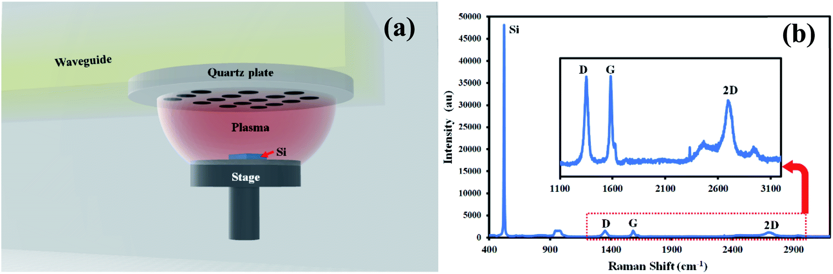 | ||
| Fig. 1 Schematic diagram of microwave plasma CVD and Raman spectrum of the corresponding graphene. | ||
2.2 Carbon dot synthesis and purification
5 gm of citric acid was dissolved in 15 ml of NaOH–ethanol solution (1 M NaOH![[thin space (1/6-em)]](https://www.rsc.org/images/entities/char_2009.gif) :absolute ethanol in ratio 1:1). The solution was heated at 200 °C on a hot plate till an orange color solution was obtained. 15 ml of 1 M NaOH was added dropwise to this orange solution under stirring conditions. This finally obtained solution was dialyzed against distilled water for 6 hours to get pure carbon dots. The solution in the beaker was dried at 60 °C in Petri plates for 8–10 hours to obtain dry powder from carbon dots.
:absolute ethanol in ratio 1:1). The solution was heated at 200 °C on a hot plate till an orange color solution was obtained. 15 ml of 1 M NaOH was added dropwise to this orange solution under stirring conditions. This finally obtained solution was dialyzed against distilled water for 6 hours to get pure carbon dots. The solution in the beaker was dried at 60 °C in Petri plates for 8–10 hours to obtain dry powder from carbon dots.
2.3 Doping study
The carbon dots were dissolved in different solvents (ethanol, methanol, acetone, and nitromethane) at the concentration of 1 mg ml−1 and the solution thus formed was added dropwise on the graphene surface subjected to a laser beam illumination for 1 minute. The sample was rinsed lightly in the corresponding solvent and dried at 100 °C for 1 minute. NUV101E Nichia Ltd. LASER with wavelength 400–406 nm (consisting of LD Slot Module generating up to 10 W by bundling 20 fibers coupled laser diodes) was used with a diverging lens having a divergence angle 8° to irradiate silicon samples during graphene doping with C-dots. Using a diverging lens with laser restricts localized heating of the silicon surface, because of which the bulk resistance and surface morphology of the silicon substrate remains unchanged. Laser spot size was 1 × 1 cm (area 1 cm2). Hall measurements were performed before and after the doping process.2.4 Characterization
The graphene sample and carbon dots were analyzed with UV-Vis spectrophotometer (V-770), Fourier Transform Infra-red spectroscopy (FTIR) (Jasco 4700), and Raman spectroscopy having a laser excitation energy of 532 nm in Renishaw In Via Laser Raman Microscope. Size and crystallinity of the carbon dots were observed using TEM (JEOL 2100F). Hall effect measurements were performed using Lakeshore 8400 Series (Toyo Corporation, Japan) with the van der Pauw technique. Morphological survey of graphene before and after doping was done by JSM-7001F – A field emission scanning electron microscope (FE-SEM) irradiates the surface of a sample with an electron beam, detects the bounced electrons, and observes the sample.3. Results and discussion
3.1 Synthesis of graphene and C-dots
Silicon sample was examined with Raman spectroscopy after the deposition process. Fig. 1b shows a typical Raman spectrum of graphene on silicon formed in microwave plasma CVD. Prominent G, 2D peaks can be observed in the spectrum with a D-peak confirming the formation of graphene on silicon samples. As-synthesized graphene contains defects confirmed by d-peak in the Raman spectra hindering mobility. These defects might be caused by various defect sites, smaller grain sizes, grain boundaries, etc. To enhance the mobility of as-synthesized graphene, we have used carbon dots as a medium of charge transfer among the defective sites.The synthesized and purified C-dots (mentioned in Section 2.2) are easily soluble in water and were used for further analysis. The visual observation of the C-dot solution in ambient light and UV light shows the fluorescence of carbon dots (Fig. 2a). The C-dot solution displays a bright greenish blue fluorescence in UV light. UV-Vis spectroscopy shows a distinct peak at 288 nm indicating the formation of C-dots (Fig. 2c). A single absorbance peak signifies that the structure of C-dots is compact and mostly homogenous nanoparticles are formed in the solution. An absorbance peak in the UV-region is typical for C-dots and is attributed to the n–π* transition of C![[double bond, length as m-dash]](https://www.rsc.org/images/entities/char_e001.gif) O (presence of carboxyl/hydroxyl groups) and π–π* transitions due to CC stacking.29,30 It can be observed that the background absorbance is almost nil which can be an indication of less content of impurities in the sample.
O (presence of carboxyl/hydroxyl groups) and π–π* transitions due to CC stacking.29,30 It can be observed that the background absorbance is almost nil which can be an indication of less content of impurities in the sample.
 | ||
| Fig. 2 (a) Visual observation of C-dots in ambient light and UV light (b) TEM image of C-dots (red arrow pointing C-dots) (c) UV-Vis spectrum (d) HRTEM image of a single C-dot with inter lattice spacing (0.24 nm) marked in red lines (e) FTIR of C-dots. | ||
Further morphological analysis of C-dots was performed using TEM. The aqueous solution of C-dots was coated on a TEM grid and subjected to analysis. Fig. 2b shows spherical C-dots in the range of 5–10 nm size and Fig. 2d displays a high-resolution TEM image of a single C-dot of size 6–7 nm (Fig. 2d). The inter lattice pattern is visible and constant and was found to be 0.24 nm which corresponds to the (001) facet of graphite.31–34
FTIR was also performed for investigating the functional groups attached on C-dots surface. FTIR spectra show a wide range of surface peaks. A few minor peaks were observed in the range of 3400 cm−1 to 3600 cm−1. Also, several small sharp peaks were observed between 670 cm−1 to 900 cm−1. All these peaks are attributed due to the presence of N–H stretch and primary or secondary amine groups. A sharp strong peak at 1620 cm−1 is observed due to N–H bending vibrations. These peaks mainly arise due to the precursor citric acid used for the synthesis of C-dots hence resulting in nitrogen-doped carbon dots. A wide range of small, and low-intensity peaks were observed in the range of 2500–3300 cm−1 which are visible due to the O–H stretch vibrations of carboxylic acids owing to NaOH functionalization of the C-dot surface. A sharp peak was observed at 1270 cm−1 and 1500 cm−1 which could be due to the C–H bend or C–O stretch vibrations arising from the surface passivation of dots.
3.2 Doping process
The C-dots suspended in various solvents were added dropwise onto the graphene sample and were exposed to the laser until the solvent evaporates. 1 × 1 cm van der Pauw devices were fabricated for the Hall measurements before and after the doping process and the results are presented in Table 1.| C dots dissolved in | Graphene mobility, cm2 V−1 s−1 | Carrier concentration, X 1013/cm−2 | Graphene sheet R, kΩ □−1 | |||
|---|---|---|---|---|---|---|
| Before | After | Before | After | Before | After | |
| Ethanol | 102.8 | 363 | 73.5 | 21 | 0.83 | 0.43 |
| Acetone | 1.99 | 4.7 | 110 | 42 | 2.86 | 3.16 |
| Nitromethane | 32.7 | 9.14 | 7.29 | 31.6 | 2.41 | 2.16 |
| Methanol | 33.2 | 67.4 | 32.9 | 17 | 0.57 | 0.54 |
It is clear from the table that the graphene samples treated with C-dots suspended in ethanol, acetone, and methanol show an increase in mobility and decrease in carrier concentration after the doping process. Whereas, C-dots suspended in ethanol give a three-fold increase in mobility as compared to C-dots suspended in acetone and methanol which show a two-fold increase in mobility. On the contrary, in the case of C-dots suspended in nitromethane, the mobility of the sample drastically decreases and carriers increase after the doping process. This could be a result of improper interaction of C-dots with graphene surface since C-dots are sparingly soluble in nitromethane solution and therefore, the surface groups might be partially exposed. However, C-dots suspended in ethanol, acetone, and methanol display a similar pattern of interaction with graphene surface as C-dots are easily soluble in these solvents (also, all three solvents belong to a similar group of organic compounds and the impact might be similar in the doping process).
Fig. 3a–d shows comparative Raman spectra of graphene before and after doping with C-dots dissolved in various solvents. Fig. 3a shows the evolution of the D + D′ peak after doping of graphene with C-dots dissolved in ethanol. Also, shift in the G peak of 1.4 cm−1. D/G ratios of graphene used for the doping process are 1.22, 1.33, 1.21, and 0.95 for ethanol, methanol, nitromethane, and acetone respectively and the D/G ratio of graphene after the doping process are 1.26, 1.10, 0.91 and 0.89 for ethanol, methanol, nitromethane, and acetone respectively. Similarly, the G/2D ratio of graphene used for the doping process is 1.12, 1.07, 1.41, and 1.32 for ethanol, methanol, nitromethane, and acetone, respectively, and the G/2D ratio of graphene after the doping process are 1.13, 1.44, 1.72 and 1.81 for ethanol, methanol, nitromethane, and acetone, respectively (Table 2). The shifts in D/G and G/2D peak Raman intensity ratios suggest that the graphene is successfully doped with C-dots. However, sample doped with ethanol show there is an increase in D/G ratio whereas others show a drastic decrease. Similarly, in the case of G/2D ratio, the graphene doped with C-dots in ethanol shows almost the same G/2D ratio before and after the doping process, whereas other samples show a drastic increase in the G/2D ratios. This information suggests that there could be two types of doping mechanisms in the doping process with C-dots when used with ethanol and other solvents. This can be verified with data of G-peak position shifts after the doping process. For morphological survey high-resolution SEM is performed. Fig. 3e shows as-synthesized graphene and (Fig. 3f) after doping with C-dots. SEM images reveal C-dot decoration onto graphene surface without any photochemical process due to laser irradiation.
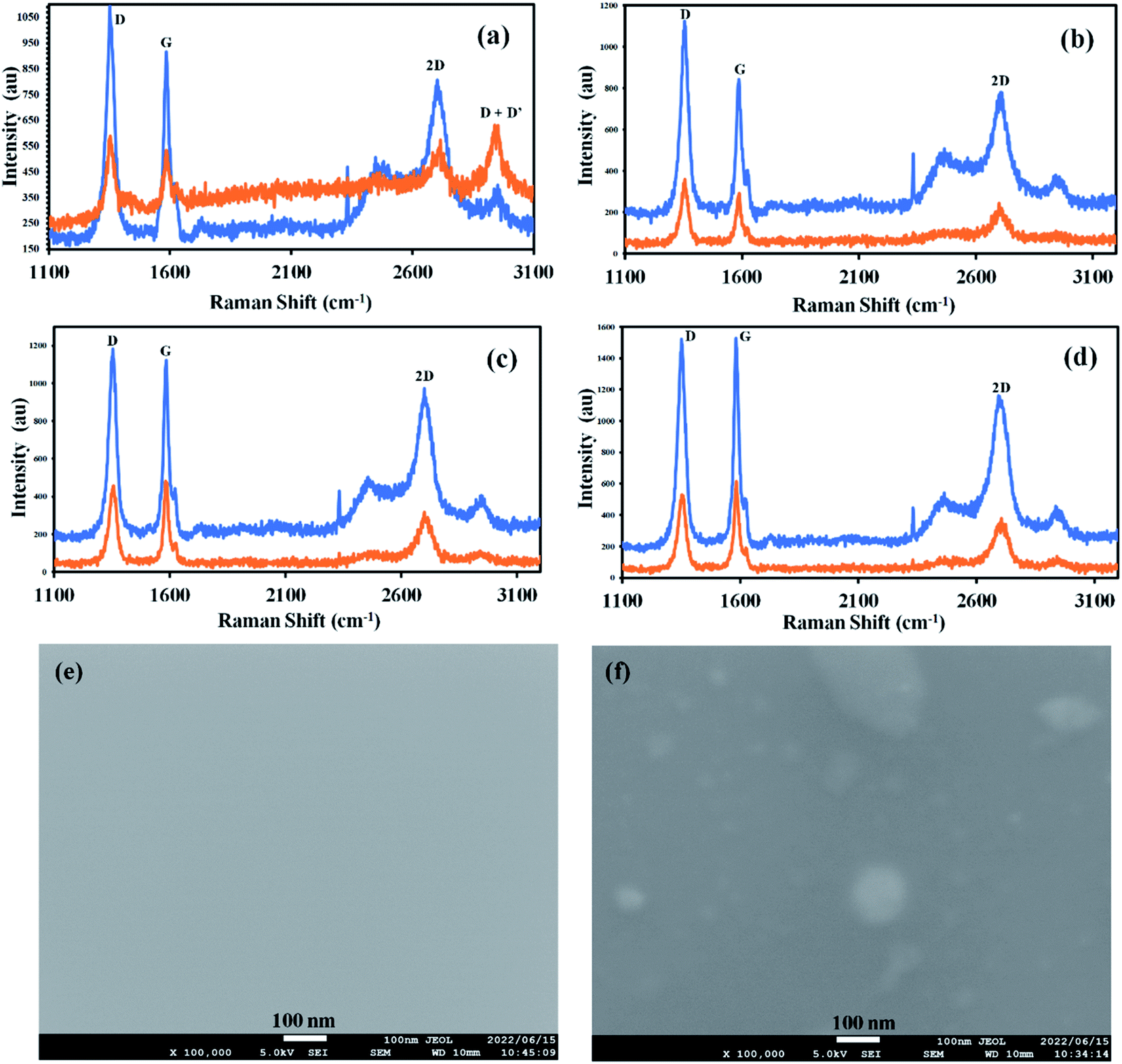 | ||
| Fig. 3 Raman spectra of graphene before (Orange) and after (Blue) doping with C-dots dissolved in (a) ethanol (b) acetone (c) nitromethane and (d) methanol, FESEM image of (e) as-synthesized graphene (f) after C-dot doping (ethanol). | ||
| Before doping | After doping | |||
|---|---|---|---|---|
| Id/Ig | I2d/Ig | Id/Ig | I2d/Ig | |
| Sample 1 | 1.22 | 0.89 | 1.26 | 0.88 |
| Sample 2 | 1.32 | 0.93 | 1.1 | 0.69 |
| Sample 3 | 1.2 | 0.71 | 0.91 | 0.58 |
| Sample 4 | 0.95 | 0.75 | 0.88 | 0.55 |
3.3 Probable mechanism
Raman spectra indicate a shift in the G-band of graphene after doping with carbon dots dissolved in various solvents. G-band is found to shift with 1.4 cm−1 towards higher energies when doped with C-dots in ethanol, whereas G-band shifts towards lower energies when doped with C-dots in acetone, nitromethane, and methanol.In doped graphene, the shift in Fermi energy can be estimated using the shift in G-peak position.35,36 The excess charge due to doping might expand or contract the crystal lattice resulting in stiffening and softening of phonons causing a shift in the G-peak position.37
Fig. 4a shows the shift in G-band by 1.4 cm−1 towards higher energy (for C-dots in ethanol labeled 1 in the figure), 0.7 cm−1 (C-dots in methanol labeled 2 in the figure), 3.5 cm−1 (C-dots in nitromethane labeled 3 in the figure) and 1.8 cm−1 (C-dots in acetone labeled 4 in the figure) towards lower energy after doping. Using the amount of G-band shift and doping carrier concentration, Fermi energies were estimated for all the samples using the graph of change in D-peak position to graphene fermi energy with graphene doping as a ref. 37. For obtaining changes in carrier concentration, Hall effect measurements were performed on all the above samples. Table 1 shows carrier mobilities and concentrations before and after the doping of graphene samples with C-dots. The change in Fermi energy for samples 1–4 was estimated to be 0.2 eV, 0.1 eV less than 0.1 eV, and less than 0.1 eV respectively, using the shift in G-peak shown in Fig. 4a.37 This information shows that the maximum change in Fermi energy is in the case of C-dots-ethanol doping of graphene, indicating higher charge transfer between graphene and C-dots. The mobility was also found to increase to 398 cm2 V−1 s−1 (stable up to one month upon repeated measurements at normal atmospheric conditions, see Fig. S1 provided in ESI†) due to such a higher shift in Fermi energy of the C-dot–graphene system. It is also observed that the 2D/G ratio is highest for C-dots–graphene, indicating better optical phonon transfer supporting the charge transfer process in the C-dots–graphene system.
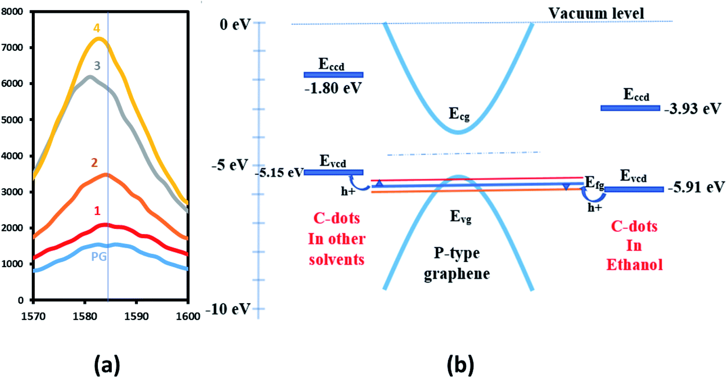 | ||
| Fig. 4 (a) Shift in G band of graphene after C-dot doping (b) band diagram. | ||
Thus, two types of doping mechanisms are observed in the C-dots–graphene system as shown in Fig. 4b. First, when C-dots act as an electron acceptor, the Fermi level of the graphene shifts down by 0.2 eV as observed with C-dots (in ethanol) graphene doping. Holes from C-dots flow into graphene increasing the p-type doping level of the graphene pushing the Fermi level to −5.7 eV from −5.5 eV. Secondly, when the C-dots act as electron donors, the Fermi level pulled up by 0.2 eV as observed in the other doping cases. For C-dots dissolved in other solvents than ethanol, the electrons flow into the graphene reducing the p-type doping level of the graphene pulling the Fermi level of graphene to −5.3 eV from −5.5 eV. The functional groups attached to C-dots might be playing a crucial role in such an up and down shift of Fermi level while doping. This information can be useful in tuning the graphene energy level for applications such as photodetectors, solar cells, gas sensors, etc.
We have also collected data on sheet resistance and mobility for the period of 30 days and the graph shows that the electronic properties of graphene remain stable up to 30 days (Fig S1†).
Researchers have attempted various growth techniques to improve the graphene mobility of transfer-free graphene. Table 3 above shows that graphene mobility of plasma CVD graphene has been increasing over the years and this work presents the highest graphene mobility for graphene grown directly on semiconducting substrate using microwave plasma CVD. The researchers have used substrates other than silicon to grow graphene, whereas graphene grown directly on silicon can be useful in many ways as reported in this work. Also, the use of C-dots for metal-free the doping of graphene can be advantageous in various applications demanding absence of metal contaminations.
4. Conclusion
Carbon dots play a crucial role in improving the mobility of graphene by shifting the Fermi level of graphene up or down by 0.2 eV depending on the functional group attached to their surfaces offering either electron or hole transfer. Change in Fermi level was calculated using G-peak shift in Raman spectra of doped graphene. Carbon dot doping also increases the 2D/G peak ratio. The highest mobility was found to be 398 cm2 V−1 s−1 stable up to 30 days at normal atmospheric conditions. Carbon dot doped graphene could lead to transfer-free, metal-free, high-mobility graphene synthesized at low temperatures using plasma CVD. Carbon dot doping can surely be used for graphene Fermi level tuning. Therefore, it could lead to desired graphene synthesis depending on the end application.Conflicts of interest
There are no conflicts to declare.Acknowledgements
The authors would like to thank The New Energy and Industrial Technology Development Organization (NEDO) Japan for partial financial support.References
- K. S. Novoselov, A. K. Geim, S. V Morozov, D. Jiang, Y. Zhang, S. V Dubonos, I. V Grigorieva and A. A. Firsov, Science, 2004, 306, 666–669 CrossRef CAS PubMed
.
- G. P. Veronese, M. Allegrezza, M. Canino, E. Centurioni, L. Ortolani, R. Rizzoli, V. Morandi and C. Summonte, Sol. Energy Mater. Sol. Cells, 2015, 138, 35–40 CrossRef CAS
- Z.-S. Wu, W. Ren, L. Gao, J. Zhao, Z. Chen, B. Liu, D. Tang, B. Yu, C. Jiang and H.-M. Cheng, ACS Nano, 2009, 3, 411–417 CrossRef CAS PubMed
- M. Pirmoradian, E. Torkan, N. Abdali, M. Hashemian and D. Toghraie, Mech. Mater., 2020, 141, 103248 CrossRef
- K. I. Bolotin, Graphene nanocomposites: A review on processes, properties, and applications, ed. V. Skákalová and A. B. B. T.-G. Kaiser, Woodhead Publishing, 2014, pp. 199–227 Search PubMed
- Y.-J. Yu, Y. Zhao, S. Ryu, L. E. Brus, K. S. Kim and P. Kim, Nano Lett., 2009, 9, 3430–3434 CrossRef CAS PubMed
- G. Anagnostopoulos, P.-N. Pappas, Z. Li, I. A. Kinloch, R. J. Young, K. S. Novoselov, C. Y. Lu, N. Pugno, J. Parthenios, C. Galiotis and K. Papagelis, ACS Appl. Mater. Interfaces, 2016, 8, 22605–22614 CrossRef CAS PubMed
- H. Murata, Y. Nakajima, N. Saitoh, N. Yoshizawa, T. Suemasu and K. Toko, Sci. Rep., 2019, 9, 4068 CrossRef PubMed
- J. H. Gosling, O. Makarovsky, F. Wang, N. D. Cottam, M. T. Greenaway, A. Patanè, R. D. Wildman, C. J. Tuck, L. Turyanska and T. M. Fromhold, Commun. Phys., 2021, 4, 30 CrossRef CAS
- A. Ismach, C. Druzgalski, S. Penwell, A. Schwartzberg, M. Zheng, A. Javey, J. Bokor and Y. Zhang, Nano Lett., 2010, 10, 1542–1548 CrossRef CAS PubMed
- R. Vishwakarma, R. Zhu, A. Mewada and M. Umeno, Nanotechnology, 2021, 32, 305601 CrossRef CAS PubMed
- M. Lu, Y. Ge, J. Wang, Z. Chen, Z. Song, J. Xu and Y. Zhao, ACS Nano, 2022, 16, 6676–6686 CrossRef CAS PubMed
- Y. Ge, L. Xu, X. Lu, J. Xu, J. Liang and Y. Zhao, Small, 2018, 14, 1–8 CAS
- A. A. Abuelwafa, R. Zhu, R. Vishwakarma, S. Elnobi, S. Adhikari, T. Soga and M. Umeno, Mater. Chem. Phys., 2021, 263, 124348 CrossRef CAS
- L. Turyanska, O. Makarovsky, L. Eaves, A. Patanè and N. Mori, 2D Mater., 2017, 4, 25026 CrossRef
- H. Fei, G. Wu, W.-Y. Cheng, W. Yan, H. Xu, D. Zhang, Y. Zhao, Y. Lv, Y. Chen, L. Zhang, C. Ó Coileáin, C. Heng, C.-R. Chang and H.-C. Wu, ACS Omega, 2019, 4, 3812–3819 CrossRef CAS PubMed
- D. Wei, Y. Liu, Y. Wang, H. Zhang, L. Huang and G. Yu, Nano Lett., 2009, 9, 1752–1758 CrossRef CAS PubMed
- F. Schedin, A. K. Geim, S. V. Morozov, E. W. Hill, P. Blake, M. I. Katsnelson and K. S. Novoselov, Nat. Mater., 2007, 6, 652–655 CrossRef CAS PubMed
- D. B. Farmer, R. Golizadeh-Mojarad, V. Perebeinos, Y.-M. Lin, G. S. Tulevski, J. C. Tsang and P. Avouris, Nano Lett., 2009, 9, 388–392 CrossRef CAS PubMed
- H. Liu, Y. Liu and D. Zhu, J. Mater. Chem., 2011, 21, 3335–3345 RSC
- H. Li, Z. Kang, Y. Liu and S.-T. Lee, J. Mater. Chem., 2012, 22, 24230–24253 RSC
- A. Mewada, S. Pandey, M. Thakur, D. Jadhav and M. Sharon, J. Mater. Chem. B, 2014, 2, 698–705 RSC
- L. Cao, X. Wang, M. J. Meziani, F. Lu, H. Wang, P. G. Luo, Y. Lin, B. A. Harruff, L. M. Veca, D. Murray, S.-Y. Xie and Y.-P. Sun, J. Am. Chem. Soc., 2007, 129, 11318–11319 CrossRef CAS PubMed
- H. Li, X. He, Z. Kang, H. Huang, Y. Liu, J. Liu, S. Lian, C. H. a Tsang, X. Yang and S.-T. Lee, Angew. Chem., Int. Ed., 2010, 49, 4430–4434 CrossRef CAS PubMed
- W. Wei, C. Xu, J. Ren, B. Xu and X. Qu, Chem. Commun., 2012, 48, 1284–1286 RSC
- L. Zhou, Y. Lin, Z. Huang, J. Ren and X. Qu, Chem. Commun., 2012, 48, 1147–1149 RSC
- L. Lin, Y. Luo, P. Tsai, J. Wang and X. Chen, Trac. Trends Anal. Chem., 2018, 103, 87–101 CrossRef CAS
- R. Vishwakarma, R. Zhu, A. A. Abuelwafa, Y. Mabuchi, S. Adhikari, S. Ichimura, T. Soga and M. Umeno, ACS Omega, 2019, 4, 11263–11270 CrossRef CAS PubMed
- Z. Luo, Y. Lu, L. A. Somers and A. T. C. Johnson, J. Am. Chem. Soc., 2009, 131, 898–899 CrossRef CAS PubMed
- G. Eda, Y.-Y. Lin, C. Mattevi, H. Yamaguchi, H.-A. Chen, I.-S. Chen, C.-W. Chen and M. Chhowalla, Adv. Mater., 2010, 22, 505–509 CrossRef CAS PubMed
- X. Y. Ren, X. X. Yuan, Y. P. Wang, C. L. Liu, Y. Qin, L. P. Guo and L. H. Liu, Opt. Mater., 2016, 57, 56–62 CrossRef CAS
- A. Kurdekar, L. A. A. Chunduri, E. P. Bulagonda, M. K. Haleyurgirisetty, V. Kamisetti and I. K. Hewlett, Microfluid. Nanofluidics, 2016, 20, 99 CrossRef
- Y. Wu, P. Wei, S. Pengpumkiat, E. A. Schumacher and V. T. Remcho, Anal. Chem., 2015, 87, 8510–8516 CrossRef CAS PubMed
- H. Liu, Z. Li, Y. Sun, X. Geng, Y. Hu, H. Meng, J. Ge and L. Qu, Sci. Rep., 2018, 8, 1–8 Search PubMed
- S. Pisana, M. Lazzeri, C. Casiraghi, K. S. Novoselov, A. K. Geim, A. C. Ferrari and F. Mauri, Nat. Mater., 2007, 6, 198–201 CrossRef CAS PubMed
- A. C. Ferrari and D. M. Basko, Nat. Nanotechnol., 2013, 8, 235–246 CrossRef CAS PubMed
- A. Das, S. Pisana, B. Chakraborty, S. Piscanec, S. K. Saha, U. V. Waghmare, K. S. Novoselov, H. R. Krishnamurthy, A. K. Geim, A. C. Ferrari and A. K. Sood, Nat. Nanotechnol., 2008, 3, 210–215 CrossRef CAS PubMed
- S. Zheng, G. Zhong, X. Wu, L. D'Arsiè and J. Robertson, RSC Adv., 2017, 7, 33185–33193 RSC
- D. Wei, L. Peng, M. Li, H. Mao, T. Niu, C. Han, W. Chen and A. T. S. Wee, ACS Nano, 2015, 9, 164–171 CrossRef CAS PubMed
- R. Vishwakarma, R. Zhu, A. A. Abuelwafa, Y. Mabuchi, S. Adhikari, S. Ichimura, T. Soga and M. Umeno, ACS Omega, 2019, 4, 11263–11270 CrossRef CAS PubMed
- Y. Okigawa, K. Tsugawa, T. Yamada, M. Ishihara and M. Hasegawa, Appl. Phys. Lett., 2013, 103, 153106 CrossRef
- N. Li, Z. Zhen, Z. Xu, R. Zhang, R. Mu and L. He, Appl. Surf. Sci. Adv., 2021, 6, 100154 CrossRef
Footnote |
| † Electronic supplementary information (ESI) available. See https://doi.org/10.1039/d2ra03274k |
| This journal is © The Royal Society of Chemistry 2022 |