
 Open Access Article
 This Open Access Article is licensed under a Creative Commons Attribution-Non Commercial 3.0 Unported Licence
Dewetting of ultrathin Ag film with random vacancy defects on a SiO2 substrate: a molecular dynamics simulation†
Lei Wang *
*
College of Mathematics and Physics, Qingdao University of Science and Technology, Shandong Advanced Optoelectronic Materials and Technologies Engineering Laboratory, Qingdao 266061, China. E-mail: Phdwangl@163.com
First published on 16th September 2022
Abstract
The spinodal instability and thermal nucleation mechanisms successfully describe the dewetting of metallic thin films. The previous research mainly focuses on homogeneous and continuous films. However, less attention is paid to the effect of random vacancy defects that frequently appear in actual situations on the film dewetting. In this work, the thermally-induced dewetting of a 0.4 nm thick ultrathin Ag film with different vacancy rate (f) ranging from 0.01 to 0.5 on a SiO2 substrate is investigated by the molecular dynamics (MD) simulation. Thermal nucleation and growth of holes appear in the dewetting process. The characteristic dewetting time (t) decreases dramatically with the increase of vacancy rate (f) of the Ag film. This is possibly because the presence of vacancy defects effectively reduce the incubation period of the initial holes, which is significant even for a very small vacancy rate less than 0.05.
Introduction
Thermally induced metallic thin film dewetting1–3 provides an efficient method to obtain spatially-correlated metallic nanoparticle arrays with characteristic length (Λ) and particle size on an inertial substrate such as SiO2 and Al2O3, which has great application potentials in molecular detection, sensing, catalysis and data storage4–6 due to its great advantages in low-cost and large-area parallel nanoparticle fabrication. The spinodal dewetting theory proposed by Vrij et al. supplies a reasonable explanation to this phenomenon, where the dewetting and rupture of a liquid thin film is originated from the competition between the stabilizing surface tension and the destabilizing long-range van der Waals attractive forces within the medium-film-substrate system.7,8 According to the spinodal theory, the characteristic length (Λ) and characteristic time (τ) of dewetting depend on the film thickness (h), but the mathematical expression depends on the particular form of the molecular interactions.2 Owusu-Ansah et al. experimentally investigated the dewetting of Pt film (3.2 nm < h < 8.9 nm) on a Ta substrate and found that L = 5.13h2.04.9 D. Schebarchov et al. used molecular dynamics to simulate the rupture of nanometre-thick liquid Au films on nanoporous substrates and found that an array of non-wettable pores can be filled by dewetting of sufficiently thin films, in which spinodal dewetting was also observed.10 In addition to the spinodal instability, the thermal nucleation is also an important mechanism to understand the film dewetting, where the hole-like patterns commonly appear in this case. J. Bischof et al. observed heterogeneous nucleation of dry circular patches in the dewetting of liquid metal film after melting with a Q-switched laser pulse, which grew in diameter during the melting period.11 T. D. Nguyen et al. performed a large-scale molecular dynamics simulations and observed the features characteristic of both spinodal instability and thermal nucleation in the spontaneously dewetting films, and they showed that these two macroscopic mechanisms share a common origin at molecular levels.12In previous studies, the author noted that the as-deposited Ag, Ni, and In metallic films on SiO2 substrates with thickness below several nanometers generally contain random vacancy defects, such as nano-sized holes and nano-islands,13,14 which is fairly common due to the well-known island growth mode.15 The vacancy defects in the film have nonnegligible effects on the dewetting process. On the one hand, the van der Waals potential between interfaces in spinodal instability is difficult to be described by a concise analytic expression in the presence of vast vacancy defects. On the other hand, the vacancy defects in the film might affect the thermal nucleation process and change the triggering condition of dewetting. Therefore, it is necessary to detailedly study the dewetting behaviour of a thin metallic film with vacancy defects on a nonwetting substrate.
In this work, dewetting of an ultrathin Ag film with random vacancy defects on a SiO2 substrate is investigated by the molecular dynamics (MD) simulation. The number of vacancy defects appearing in the film is defined and regulated by the vacancy rate (f) that is in the range of 0.01–0.5 herein. The characteristic dewetting time (t) is systematacially analysed for different f by using a Minkowski measurement. It is found that, the characteristic dewetting time (t) of the Ag film decreases dramatically with the increase of vacancy rate (f). This is possibly because the presence of vacancy defects effectively reduce the incubation period of the initial holes and thus accelerate the dewetting. This kind of dewetting acceleration effect is significant even for a very small vacancy rate less than 0.05.
Simulation method
Initial atomic model of a continuous ultrathin Ag film on SiO2 was built by Materials Studio and Large-scale Atomic/Molecular Massively Parallel Simulator (LAMMPS).16 All the following calculations were performed by LAMMPS and the complete code can be found in ESI.† The thickness of the Ag film and the SiO2 substrate was 0.4 nm and 1.6 nm, respectively. The Ag film contains 3 layers of atoms. The bottom of SiO2 substrate was fixed. The length and width of the film were both 15 nm. The size of simulation box was 15 nm × 15 nm × 10 nm, and the periodic boundary condition was adopted in three dimensions. The Tersoff potential17 and embedded-atom (EAM) potential18 were adopted to describe the Si–O and Ag–Ag interactions, respectively. The Ag–O and Ag–Si interactions were described by the Leonard Jones potential parameterized by a distance (ε) and the energy (σ) as follow,Herein, σAg–Si = 0.329 nm, εAg–Si = 0.006 eV, σAg–O = 0.278 nm, and εAg–O = 0.03 eV, referring to A. C. Ngandjong's optimized DFT calculation results.19 These parameters have been tested in this paper by comparing the contact angle of Ag on SiO2 between the simulation and the experimental data in literatures.20 Random vacancy effects were created by randomly removing small cylinders with 0.4 nm in height and 0.2 nm in radius from the 0.4 nm thick Ag film by using a LAMMPS code. The vacancy rate (f) is defined as the number ratio of the surviving Ag atoms to the initial Ag atoms, which is tailored in the range from 0.01 to 0.5. The energy minimization of the system was implemented with LAMMPS by using the conjugate gradient method to achieve stable structures, where the stopping tolerance for energy was 10−10 and the stopping tolerance for force was 10−10 eV Å−1.
The initial temperature of the simulation is 300 K. The whole system was firstly heated from 300 K to 1500 K within 10 ps in NVT ensemble. Then, the heat preservation was implemented for 1 ns at 1500 K in NVT ensemble. The time step in simulation is 1 fs. The Nose–Hoover thermostat was adopted and the temperature damping parameter (Δt) was 0.1 ps (namely 100 timesteps) that was recommended by LAMMPS. Besides, the effect of temperature damping parameters (0.01 ps, 0.1 ps, and 1 ps) on the film dewetting time was inapparent (Fig. S1†). The film-substrate system with no atomic vacancy contains 37![[thin space (1/6-em)]](https://www.rsc.org/images/entities/char_2009.gif) 906 atoms, where the SiO2 substrate contains 27540 atoms. The dewetting patterns over time were displayed with OVITO. By using the image processing software ImageJ, the top-view dewetting patterns were transformed into 8 bit greyscale images. Then, the area ratio (St) of the dewetted Ag to the initial Ag film was calculated at each moment using ImageJ to quantificationally estimate the dewetting evolution, which is a simplified Minkowski measure method.21 As for the final stable dewetted patterns at 300 ps, the area ratio is S′. Herein, the characteristic dewetting time (t) was defined as the earliest moment when∣(St − S′)/S′| < 10% is satisfied.
906 atoms, where the SiO2 substrate contains 27540 atoms. The dewetting patterns over time were displayed with OVITO. By using the image processing software ImageJ, the top-view dewetting patterns were transformed into 8 bit greyscale images. Then, the area ratio (St) of the dewetted Ag to the initial Ag film was calculated at each moment using ImageJ to quantificationally estimate the dewetting evolution, which is a simplified Minkowski measure method.21 As for the final stable dewetted patterns at 300 ps, the area ratio is S′. Herein, the characteristic dewetting time (t) was defined as the earliest moment when∣(St − S′)/S′| < 10% is satisfied.
Results and discussion
Fig. 1a shows the model of a 0.4 nm thick Ag film without defects on the SiO2 substrate after energy minimization in LAMMPS. After a temperature rise from 300 K to 1500 K in 10 ps and the following heat preservation for 1 ns at 1500 K above its melting point, a single Ag particle was formed in consideration of the periodic boundary condition adopted (Fig. 1b). In the side view of the dewetted Ag particle on SiO2 (Fig. 1c), a contact angle of 136° is observed that is close to experimental data ∼140° reported in literatures.20 Therefore, the adopted potential functions and simulation methods are reasonable in this paper.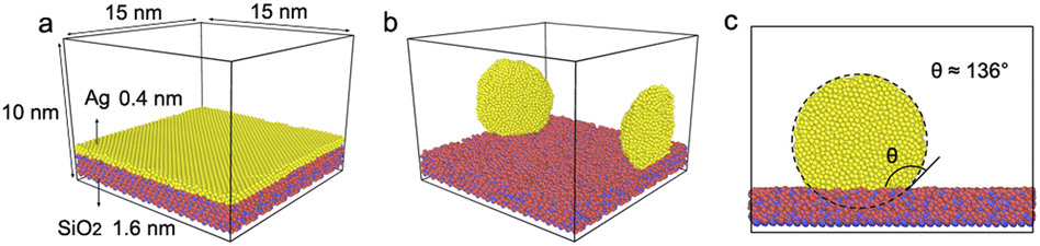 | ||
| Fig. 1 (a) Simulation model of the 0.4 nm thick Ag film without vacancy defects on SiO2 before heating; (b) dewetted pattern of the Ag film after heating for 1 ns at 1500 K; (c) side view of the dewetted pattern and the contact angle is shown. | ||
Fig. 2a–i show the time-dependent dewetting evolution of the Ag thin film without vacancy defects within 300 ps. The Ag thin film is rapidly liquefied and becomes disordered through heating. In this process, some atomic vacancy defects arise (circle A in Fig. 2b) and also disappear randomly, and a few vacancy defects can form small initial holes (circle B in Fig. 2c). Such an initial hole will rapidly grow (circle C in Fig. 2d) and finally rupture the film. Thermal nucleation and growth of holes are clearly shown in the above film dewetting process. In order to quantitatively describe this process, 8 bit greyscale images at each moments were obtained as shown in Fig. 2j as an example, and then the area ratio (St) of the dewetted Ag to the initial Ag film was calculated from 0 ps to 300 ps (Fig. 2k). As shown in Fig. 2k, St firstly presents a plateau and secondly shows a dramatic decrease, and finally achieves a stable value. In fact, the variation of St completely describe the film dewetting. The plateau of St corresponds to the incubation period (τ0) of an initial hole, which is about 100 ps (Fig. 2k) for the perfect Ag film (Fig. 2a). The dramatic decrease stage of St corresponds to the hole growth and film rupture process from 110 ps (Fig. 2d) to 240 ps (Fig. 2h). After t = 240 ps, the variation of dewetting patterns is unconspicuous and the stable pattern is achieved at 300 ps, namely S′ = 19.0 (Fig. 2k). Because the error between St (240 ps) and S′ is less than 10%, the characteristic dewetting time (t) of the Ag film without vacancy defects is 240 s according to the definition stated in the section of Simulation method.
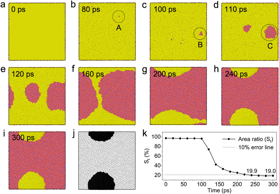 | ||
| Fig. 2 (a–i) Time-dependent dewetting patterns of the Ag film without vacancy defects from 0 ps to 300 ps; (j) the 8-bit grayscale image corresponding to (i); (k) the function of area ratio St versus time. | ||
As shown in Fig. 3a, the vacancy defects were introduced into the initial Ag thin film by randomly removing small cylinders with 0.2 nm in radius from the film, where the distances between adjacent removed cylinders are totally random. The vacancy rate (f) is defined as the number ratio of the surviving Ag atoms to the initial Ag atoms. It should be noted that the heights of the film and the cylinder are both 0.4 nm containing 3 layers of Ag atoms, which can be proved by the film morphologies as shown in panel I of Fig. 3b–e before the procedure of energy minimization. After the energy minimization in LAMMPS, stable film structures with different f are obtained, where some vacancy defects vanish and some grow in volume. As shown in panel II of Fig. 3b–d with f ≤ 0.5, the stable Ag film is connected inside. This kind of film structure is very common in real metallic nano-films prepared by magnetron sputtering, electronic beam evaporation and other techniques, which will rupture in film dewetting. This kind of film is the focus of this paper. Besides, when f > 0.5, as shown in panel II of Fig. 3e, the film gradually becomes island shaped. This kind of island-shaped film generally presents also an aggregation behaviour in addition to rupture in film dewetting, thus it is not the focus of this paper. As for the Ag film with f ≤ 0.5 after energy minimization, the atom number density along the thickness direction is calculated (Fig. 3f). The decrease of atom number density for 0.01 ≤ f ≤ 0.5 is mainly due to the existence of vacancy defects. The height of top layer is about 5.5 nm and its atom number density shows a monotone decrease with an increase in f. By comparing the three peaks of the atom density, the atoms on top layer are more easily to migrate from their initial positions. In this work, the film after energy minimization with LAMMPS shown in panel II of Fig. 3 was considered as the initial stage in film dewetting. It should be noted that, this initial pattern may not be universal since the distribution of vacancies may have some spatial bias during the real fabrication by different techniques although the actual process leads to the same overall vacancy rate of the random distribution in panel I, which the author defines as the number ratio of the surviving Ag atoms to the initial Ag atoms.
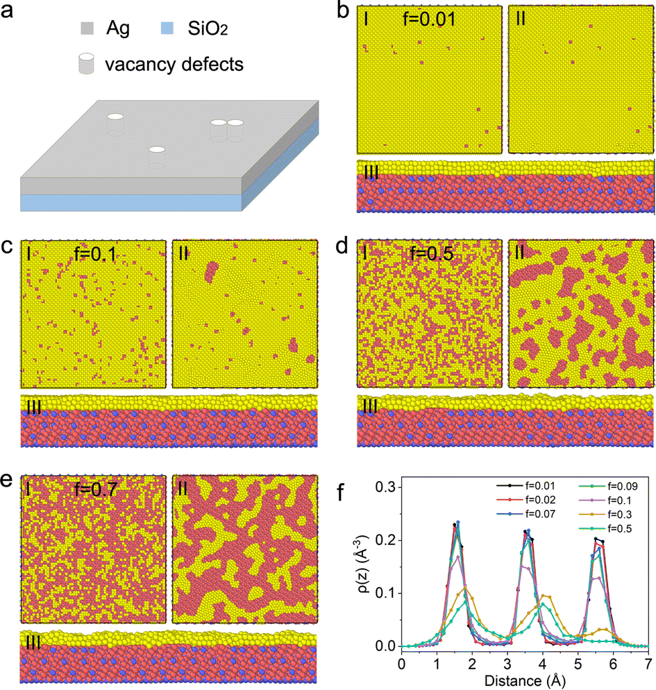 | ||
| Fig. 3 (a) Schematic diagram of the Ag film with random vacancy defects; (b–e) simulation models of the Ag films with f = 0.01, 0.1, 0.5 and 0.7, respectively. Panel I is the initial film structure with vacancy defects without energy minimization, panel II is the stable film structure with vacancy defects after energy minimization with LAMMPS, and panel III is the side view of panel II; (f) The atom number density of Ag along the thickness direction, and the zero point refers to the bottom of a Ag film. | ||
Fig. 4 detailedly display the time-dependent film dewetting evolution for different f. The case of f = 0 has been analysed above. As shown in Fig. 4b, for f = 0.01, the vacancy defects disappear within 40 ps (Fig. 4b(II)) rather than directly form a hole. As shown in Fig. 4b(IV), the incubation period (τ0) of its initial hole is less than 100 ps that is shorter than the case of f = 0 by comparing Fig. 4a(IV) and b(IV). For f = 0.02, the vacancy defects also disappear within 40 ps, but the incubation period (τ0) of its initial hole further reduces to less than 80 ps. For f > 0.04, the area of vacancy defects is large, in which case, the initial hole is directly formed with a negligible τ0 and fast film rupture happens. Obviously, the characteristic dewetting time (t) shows a significant decrease when f increases from 0 to 0.5 (Fig. 4a–g).
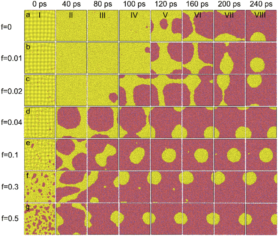 | ||
| Fig. 4 The dewetting pattern evolution over time of the Ag film with different f of 0 (a), 0.01 (b), 0.02 (c), 0.04 (d), 0.1 (e), 0.3 (f) and 0.5 (g). | ||
Similar to Fig. 2k, the functions of area ratio (St) versus time are also obtained for different f ranging from 0 to 0.5. As shown in Fig. 5a, when f increases from 0 to 0.1, the plateau of the plot becomes shorter and in other words the incubation period (τ0) of its initial hole gradually shortens. The decrease of τ0 dramatically accelerate the film dewetting process, which is also clearly revealed in Fig. 4. As shown in Fig. 5b, the characteristic dewetting time (t) rapidly decreases from 240 ps down to 120 ps for 0 < f< 0.1. For f = 0.4 and f = 0.5, the characteristic dewetting time (t) is only about 80 ps.
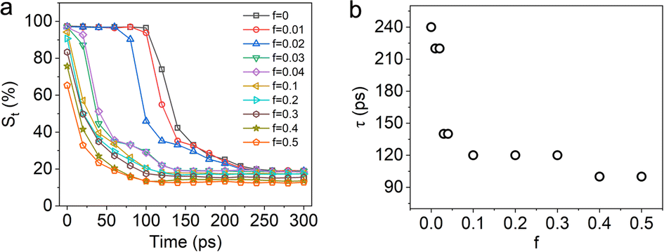 | ||
| Fig. 5 (a) The function of area ratio St versus time with different f; (b) the characteristic dewetting time (t) of the 0.4 nm thick Ag film with different f. | ||
In this simulation work, the spatially-correlated particle array was not observed in the film dewetting process. The interaction between the Ag film and the SiO2 substrate is relatively weak compared with the surface tension within the Ag film, in which case, the characteristic length (or the particle distance) in film dewetting tends to be a large value. This might be able to explain the formation of final single drop for all cases in the simulation using a small model with a transverse size of 15 nm. The author speculates that a spatially-correlated particle array will be observed if a larger model is adopted in the simulation. Previous experimental and theoretical researches indicate that the characteristic dewetting time (t) depends on the film thickness. This work further shows that vacancy defects contained in the film also have significant effect on τ, even if the vacancy rate (f) is less than 0.05. Actually, vacancy defects exist widely in a real thin metallic film system and this effect might describe a more realistic dewetting process thus has practical significances. The simulation indicates that the incubation period of an initial hole reduces dramatically with an increase in f, which might be a key point that speeds up the film dewetting. This result also confirms the importance of thermal nucleation of holes in a film dewetting process. Besides, the nanosecond laser pulse is generally regarded as a necessity to trigger metallic film dewetting.2,22 However, this simulation indicates that a picosecond laser pulse might be also an possible heating tool to achieve thin film dewetting in the presence of vast vacancy effects.
Conclusions
This work investigates the effect of vacancy defects on the thermal-induced dewetting process of a 0.4 nm thick Ag film on a SiO2 substrate by MD simulations with LAMMPS. The variation of vacancy rate (f) is in the range from 0.01 to 0.5. The dewetting process is quantitatively described by the function of the dewetting pattern area versus time, which is a Minkowski measure. The simulation indicates a significant reduction of the characteristic dewetting time (t) with an increase in vacancy rate. This effect might be originated from the reduction of the incubation period of initial holes in the presence of vacancy defects. This simulation describes a more realistic dewetting process of a thin metallic film with widely existed vacancy defects, which has practical guiding significances.Conflicts of interest
There are no conflicts to declare.Acknowledgements
The work was supported by the Natural Science Foundation of Shandong Province, grant number ZR2021QF003, and the research start-up fund of QUST, grant number 1203043003591.References
- J. Ye, D. Zuev and S. Makarov, Int. Mater. Rev., 2018, 64, 439–477 CrossRef.
- L. Kondic, A. G. González, J. A. Diez, J. D. Fowlkes and P. Rack, Annu. Rev. Fluid. Mech., 2019, 52, 235–262 CrossRef.
- D. Gentili, G. Foschi, F. Valle, M. Cavallini and F. Biscarini, Chem. Soc. Rev., 2012, 41, 4430–4443 RSC.
- S. Hsu, A. L. Rodarte, M. Som, G. Arya and A. R. Tao, Chem. Rev., 2018, 118, 3100–3120 CrossRef CAS PubMed.
- C. Zong, M. Xu, L. Xu, T. Wei, X. Ma, X. Zheng, R. Hu and B. Ren, Chem. Rev., 2018, 118, 4946–4980 CrossRef CAS PubMed.
- J. Yang, Y. Chen, T. Huang, H. Duan, N. Thiyagarajah, H. Hui, S. H. Leong and V. Ng, Nanotechnology, 2011, 22, 385301 CrossRef PubMed.
- A. Vrij, Discuss. Faraday Soc., 1966, 42, 23–33 RSC.
- R. Xie, A. Karim, J. F. Douglas, C. C. Han and R. A. Weiss, Phys. Rev. Lett., 1998, 5, 1251–1254 CrossRef.
- E. Owusu-Ansah, V. I. Birss and Y. Shi, J. Phys. Chem. C, 2020, 124, 23387–23393 CrossRef CAS.
- D. Schebarchov, B. Lefèvre, W. R. C. Somervillea and S. C. Hendy, Nanoscale, 2013, 5, 1949 RSC.
- J. Bischof, D. Scherer, S. Herminghaus and P. Leiderer, Phys. Rev. Lett., 1996, 77, 1536–1539 CrossRef CAS PubMed.
- T. D. Nguyen, M. Fuentes-Cabrera, J. D. Fowlkes and P. D. Rack, Phys. Rev. E, 2014, 89, 032403 CrossRef PubMed.
- L. Wang, X. Wang, X. Wang and Q. Liu, Appl. Surf. Sci., 2020, 527, 146771 CrossRef CAS.
- L. Wang, X. Chi, X. Wang, Q. Liu and L. Sun, Appl. Surf. Sci., 2020, 506, 144705 CrossRef CAS.
- N. Kalfagiannis, A. Siozios, D. V. Bellas, D. Toliopoulos, L. Bowen, N. Pliatsikas, W. M. Cranton, C. Kosmidis, D. C. Koutsogeorgis, E. Lidorikisb and P. Patsalas, Nanoscale, 2016, 8, 8236 RSC.
- S. Plimpton, J. Comput. Phys., 1995, 117, 1–19 CrossRef CAS.
- S. Munetoh, T. Motooka, K. Moriguchi and A. Shintani, Comput. Mater. Sci., 2007, 39, 334–339 CrossRef CAS.
- P. L. Williams, Y. Mishin and J. C. Hamilton, Model. Simul. Mater. Sci., 2006, 14, 817–833 CrossRef CAS.
- A. C. Ngandjong, C. Mottet and J. Puibasset, J. Phys. Chem. C, 2016, 120, 8323–8332 CrossRef CAS.
- N. Eustathopoulos, B. Drevet and M. L. Muolo, Mater. Sci. Eng. A, 2001, 300, 34–40 CrossRef.
- K. Jacobs and S. Herminghaus, Langmuir, 1998, 14, 965–969 CrossRef CAS.
- D. Qi, S. Huang, L. Wang, M. Shi, S. Chen and C. P. Grigoropoulos, Mater. Lett., 2018, 211, 250–253 CrossRef CAS.
Footnote |
| † Electronic supplementary information (ESI) available. See https://doi.org/10.1039/d2ra03137j |
| This journal is © The Royal Society of Chemistry 2022 |