DOI:
10.1039/D2RA03053E
(Paper)
RSC Adv., 2022,
12, 22188-22196
First-principles investigation on the electronic structures of CdSexS1−x and simulation of CdTe solar cell with a CdSexS1−x window layer by SCAPS†
Received
14th May 2022
, Accepted 3rd July 2022
First published on 10th August 2022
Abstract
The short-circuit current density (JSC) of CdTe solar cells both in the short and long wavelength regions can be effectively enhanced by using CdS/CdSe as the composite window layer. CdS/CdSe composite layers would interdiffuse to form the CdSexS1−x ternary layer during the high temperature deposition process of CdTe films. In this paper, the electronic properties of CdSexS1−x (0 ≤ x ≤ 1) ternary alloys are investigated by first-principles calculation based on the density functional theory (DFT) and the performance of CdS/CdSe/CdTe devices are modeled by SCAPS to reveal why CdS/CdSe complex layers have good effects. The calculation results show that the position of the valence band of CdSexS1−x moves towards the vacuum level as the doping concentration of Se increases and the band gap becomes narrow. According to device modeling, the highest conversion efficiency of 20.34% could be achieved through adjusting the conduction band offset (CBO) of theCdSexS1−x/CdTe interface to about 0.11 eV while the Se concentration x approaches 0.75. Further investigations suggest a 50–120 nm thickness of CdSexS1−x (x = 0.75) would obtain better device performance. It means that solar cells with a CdSexS1−x/CdTe structure need a suitable Se content and thickness of CdSexS1−x. These results can provide theoretical guidance for the design and fabrication of high efficiency CdTe solar cells.
1. Introduction
Cadmium telluride (CdTe) solar cells are some of the most representative thin-film solar cells, characterized by high efficiency and low-cost. The conversion efficiency of CdTe solar cells has dramatically improved from 17.3% (2011)1 to 22.1% (2016).2 Studies show that this rapid progress has mainly resulted from enhancements in short-circuit current density (JSC), both in the short and long wavelength regions, by optimizing the window layers.3,4 Typically, CdTe solar cells use n-CdS window layers to form hetero-junctions.5 However, CdS has a band gap (Eg) of 2.4 eV, and large lattice mismatch of 11% with the CdTe layer,6 which result in a deficit in the JSC and open circuit voltage (VOC). Commonly, one way to enhance the JSC is to use wider band-gap transparent conducting oxides (TCOs) instead of CdS as the window layer or as high-resistance transparent (HRT) films. Another way is to employ compound window layers for reducing the thickness of the CdS layer. Previously, some new types of window layers with wider band gap such as CdS:O, Zn1−xMgxO (ZMO), and Cd1−xZnxS have been applied in CdTe solar cells to enhance the short-wavelength quantum efficiency (QE).7,8 In our prior work,9 using the SCAPS program, we demonstrated higher JSC in a ZMO window layer than in CdS due to its wide band gap, which was consistent with the experimental results.10 Despite the impressive ZMO/CdTe solar cell improvement compared with CdS/CdTe, the conversion efficiency is still only ∼18%.
CdSe is a classic semiconductor with a direct band gap of 1.69 eV which has little size mismatch with CdTe and therefore has a high solubility in CdTe.11,12 In recent years, using CdSe as the window layer in CdTe solar cells has been reported. Paudel et al.3 reported that the spectral response can be enhanced in short wavelength regions by using CdSe film instead of CdS as the CdTe solar cell window layer. The JSC was improved by about 2 mA cm−2 compared with the CdS control. However, the open-circuit voltage (VOC) decreased by about 40 mV. We fabricated CdSe films by sputtering at various temperatures and applied them in CdTe solar cell.13 The results indicate that the QE of CdSe/CdTe solar cell was enhanced in the range of 300–510 nm, but the VOC is only about 725 mV, resulting in the efficiency only about 12%. The experimental results10 demonstrate that using a composite CdS/CdSe window layer is an effective method to obtain both high VOC and Jsc. In fact, CdS/CdSe layers would transform to CdSexS1−x layer by interdiffusion due to the high deposition temperature of CdTe films. So in this study, we tried to find why CdS/CdSe complex layers have good effects by calculating the electronic properties of CdSexS1−x using first-principles method based on the density functional theory (DFT) and modeling the performance of CdS/CdSe/CdTe devices by SCAPS program.
SCAPS is a one-dimensional solar cell simulation program. It is a powerful program to model the performance of the solar cells, which is developed by the Burgelman group of the University of Ghent in Belgium.14 SCAPS is widely used to simulate the device parameters of CIGS,15,16 CZTS17,18 and CdTe19,20 solar cells. Most of the simulation results are consistent with the experimental performances and provide important indications for experimental work. Here, we focused on the effects of Se contents on the band structure of CdSexS1−x and compared with the experimental results. The dependence of CdTe solar cell performances on the Se composition x and various thicknesses of CdSexS1−x are also investigated.
2. Theoretical model and calculation methods
2.1 Theoretical model
In the package, we consider a 2 × 2 × 2 supercell of a cubic zinc blende structure CdS, which contains 64 atoms (32 Cd atoms and 32 S atoms), as shown in Fig. 1. The crystal structures of CdS, CdSe are shown in Fig. S1,† while the crystal structures of CdSexS1−x (x = 0.25, 0.5, 0.75) are shown in Fig. S2.† In our current work we consider only substitutional doping with Se atoms substituting S atoms in CdS. The CdSexS1−x system corresponds with Se dopant concentration of x = 0, 0.25, 0.5, 0.75, 1, respectively. Normally, there are many equivalent substitution possibilities for a particular structure. Nevertheless, spatial symmetry exists in crystal structure, configuration of alloy substitution can be found using crystal symmetry and periodic translation feature. For the considered structures, the optimization is performed by minimizing the total energy with respect to obtain the most stable conformation. All electronic properties are calculated on the basis of the most stable structure.
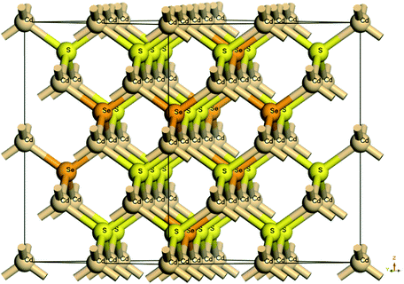 |
| | Fig. 1 Crystal structure of cubic zinc blende CdSexS1−x supercell and doping position. | |
The baseline model structure of CdTe solar cells used in the simulation consisted of SnO2![[thin space (1/6-em)]](https://www.rsc.org/images/entities/char_2009.gif) :F (FTO) layer, CdS window layer, CdTe absorb layer and ZnTe:Cu back contact. A defect density of 5 × 1016 cm−3 was chosen for the CdS layer.19 In the advanced device structure, CdSexS1−x replaces CdS film as the window layer of CdTe solar cells, as shown in Fig. 2. The layer of CdSexS1−x ternary compound, resulting from the diffusion of CdS and CdSe during the fabrication processes of heat treatment or CdCl2 treatment, formed between the CdS and CdSe layers has been reported.3 This model is a simplification of the actual cells and ignore phenomena related to polycrystallinity, such as the loss of surface reflection. Furthermore, the facts that light is absorbed in the transparent conductive film and window layer, and all the incident light passes through to the absorption layer are also neglected.
:F (FTO) layer, CdS window layer, CdTe absorb layer and ZnTe:Cu back contact. A defect density of 5 × 1016 cm−3 was chosen for the CdS layer.19 In the advanced device structure, CdSexS1−x replaces CdS film as the window layer of CdTe solar cells, as shown in Fig. 2. The layer of CdSexS1−x ternary compound, resulting from the diffusion of CdS and CdSe during the fabrication processes of heat treatment or CdCl2 treatment, formed between the CdS and CdSe layers has been reported.3 This model is a simplification of the actual cells and ignore phenomena related to polycrystallinity, such as the loss of surface reflection. Furthermore, the facts that light is absorbed in the transparent conductive film and window layer, and all the incident light passes through to the absorption layer are also neglected.
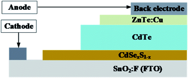 |
| | Fig. 2 Device structure of CdTe solar cell for the numerical simulation. | |
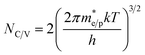
Relevant electric and optical parameters employed are summarized in Table 1 and the majority of input parameters for the simulations were mainly collected from relevant theories, the literature7,15,19,21 or estimated in a reasonable range, etc. Constrained to the more reasonable ranges of the experimental date for the typical CdTe solar cells, the defect density of 1 × 1016 cm−3 for the CdSexS1−x layer is selected.15 Properties of other layers as well as the neutral interface defects are kept from the baseline CdS/CdTe model. Density of states at the conduction band minimum (NC) and valence band maximum (NV) are calculated using eqn (1):15
| |
 | (1) |
where

are the effective masses of electrons/holes,
h is Planck's constant and
k is the Boltzmann constant. Thermal velocities for electrons (
ve) and holes (
vp) are obtained from the
eqn (2):
15| |
 | (2) |
Table 1 Simulation parameters for the baseline model of CdTe solar cellsa
| Layer properties |
FTO15 |
CdSexS1−x |
CdTe14 |
ZnTe:Cu15 |
| x = 0 (ref. 8) |
x = 0.25 |
x = 0.5 |
x = 0.75 |
x = 1 |
| ε/ε0: relative permittivity; Nc: effective density of states in conduction band; Nv: effective density of states in valence band; μn: electron mobility; μp: hole mobility; Ve: recombination velocity of electrons; Vp: recombination velocity of holes; NA: carrier concentration; n: effective carrier concentration of n-type semiconductor layers; p: effective carrier concentration of p-typed semiconductor layers. |
| Eg/eV |
3.65 |
2.42 |
2.21 |
2.02 |
1.89 |
1.73 |
1.45 |
2.26 |
| ε/ε0 |
8.9 |
9 |
9 |
9 |
9 |
9 |
10 |
10.1 |
| Nc/cm−3 |
5.2 × 10¹⁸ |
2.2 × 10¹⁸ |
1 × 10¹⁸ |
1 × 10¹⁸ |
1 × 10¹⁸ |
1 × 10¹⁸ |
9.2 × 10¹⁷ |
1.5 × 10¹⁸ |
| Nv/cm−3 |
1.0 × 10¹⁹ |
1.8 × 10¹⁹ |
1.5 × 10¹⁹ |
1.5 × 10¹⁹ |
1.5 × 10¹⁹ |
1.5 × 10¹⁹ |
5.2 × 10¹⁸ |
1.16 × 10¹⁹ |
| μn/cm2 v−1 s−1 |
100 |
340 |
300 |
300 |
300 |
300 |
400 |
400 |
| μp/cm2 v−1 s−1 |
25 |
50 |
50 |
50 |
50 |
50 |
60 |
50 |
| Ve/cm s−1 |
1.0 × 10⁷ |
3.1 × 10⁷ |
3.1 × 10⁷ |
3.1 × 10⁷ |
3.1 × 10⁷ |
3.1 × 10⁷ |
3.1 × 10⁷ |
1.0 × 10⁷ |
| Vp/cm s−1 |
1.0 × 10⁷ |
1.6 × 10⁷ |
1.6 × 10⁷ |
1.6 × 10⁷ |
1.6 × 10⁷ |
1.6 × 10⁷ |
1.6 × 10⁷ |
1.0 × 10⁷ |
| Carrier density/cm−3 |
n: 1 × 10²⁰ |
n: 1 × 10¹⁷ |
n: 9 × 10¹⁷ |
n: 1 × 10¹⁸ |
n: 1 × 10¹⁸ |
n: 1 × 10¹⁸ |
p: 5 × 10¹⁴ |
p: 1.5 × 10²⁰ |
| Thickness/nm |
3.5 × 10² |
100 |
100 |
100 |
100 |
100 |
5 × 10³ |
1 × 10² |
We can get the values on the effective masses of electron and hole of the CdSexS1−x layers by the first-principle, and the other layers are drawn from literature.7,9,19,21 The simulated CdS/CdTe solar cell efficiency is close to the results that calculated by using the SCAPS software.19
2.2 Computational method
The crystal structure and electronic properties of the CdSexS1−x (0 ≤ x ≤ 1) ternary mixed crystals are performed using the Cambridge serial total energy package (CASTEP) code,22 which is based on DFT using ultrasoft pseudopotentials method. The exchange-correlation potential is described by the Perdew–Burke–Ernzerhof (PBE) scheme in the GGA. The self-consistent field (SCF) tolerance and energy cutoff are 1.0 × 10⁻⁶ eV per atom and 300 eV, respectively. For the k-point, a 2 × 2 × 2 Monkhorst–Pack scheme has been used. It is well known that the DFT-GGA underestimates the band-gap of semiconductors.23 To modify the Coulomb occupation potential between electrons, the U values obtained are: Ud,Cd = 5 eV and Up,S = 4 eV.23
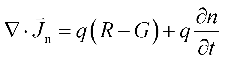
The basic principle of SCAPS software is to solve the Poisson and the continuous equations of current under these constraints according to the structural of solar cell and the input material parameters, as shown in the follow three eqn (3)–(5).
| | |
∇⋅ε∇φ = −q(p − n) + ND − NA
| (3) |
| |
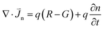 | (4) |
| |
 | (5) |
where
ε is permittivity,
φ is potential,
q is electric quantity,
p is free carrier hole concentration,
n is electron concentration,
ND is donor concentration,
NA is acceptor density,

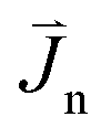
is electron current density,

is hole current density,
R and
G represent the recombination and generation rate of electron hole pairs, respectively. By setting the parameters of material and the corresponding boundary conditions, SCAPS solves the above equations by numerical calculation, and obtains the related characteristics of the solar cells.
3. Results and discussion
3.1 Structural and electronic properties of CdSexS1−x films
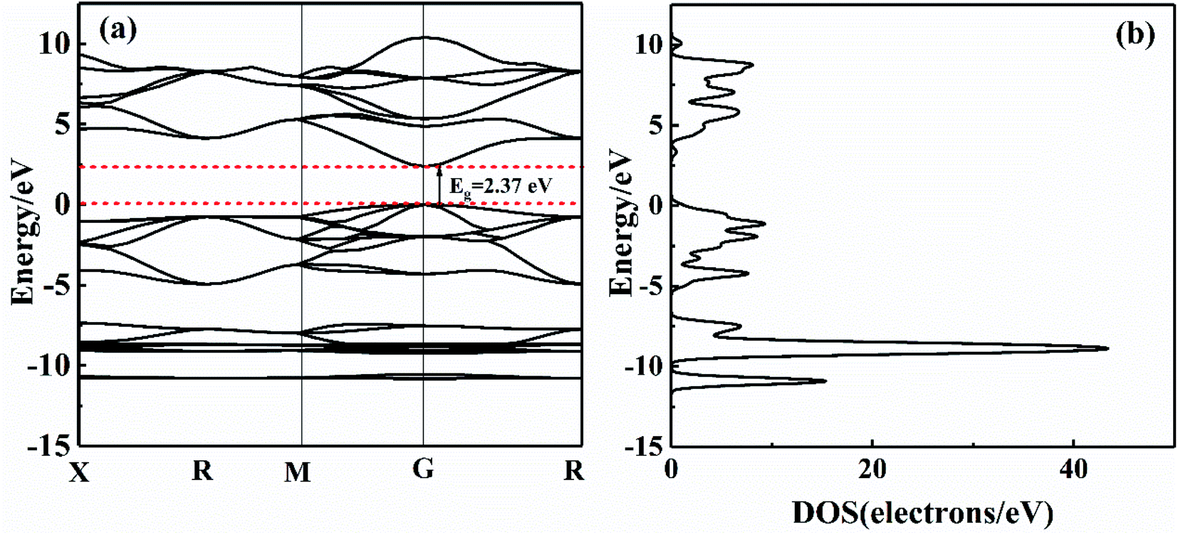
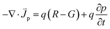
The band gap (Eg) and total state density (TDOS) of zinc blende structure CdS are shown in Fig. 3. The calculation result indicates that the direct band gap is about 2.37 eV at the highly symmetric G point, which is close to the experimental value of 2.4 eV.13 Meanwhile, as listed in Table 3, the calculated lattice parameters are almost the same as the experimental results, and it indicates that the GGA + U calculation applied in this work can explain the properties of CdS to some extent. It is clearly seen from the Fig. 3(a) that TDOS of CdS is considered of three parts of valence band and one part of conduction band, and corresponding to band gaps in Fig. 3(a), respectively. Table 2 gives CdS characteristic energy values at the conduction band minimum (ECBM) and the valence band maximum (EVBM) at each highly symmetric point in the first Brillouin zone. The width of conduction band bottom is 3.02 eV (5.39–2.37 = 3.02 eV) and the width of valence band top is 1.12 eV (1.12–0 = 1.12 eV). It indicates that non-local density of conduction band bottom of CdS is large. Therefore, the effective mass of electron is smaller than the effective mass of hole at the top of the valence band.
 |
| | Fig. 3 Calculated (a) band structure and (b) DOS of pure CdS. | |
Table 2 The values of conduction band and valence at the high symmetry points of Brillouin zone
| |
X |
R |
M |
G |
R |
| Ec/eV |
4.81 |
4.21 |
5.39 |
2.37 |
4.21 |
| Ev/eV |
−1.12 |
−0.82 |
−0.92 |
0 |
−0.82 |
Table 3 Calculated lattice parameters and band gaps of CdSexS1−x alloy
| Compounds |
x |
Lattice parameters (Å) |
Band gap energy (eV) |
| Our work |
Exp. |
Other cal. |
Our work |
Exp. |
Other cal. |
| GGA + U |
GGA |
GGA + U |
| Ref. 24 Exp. Ref. 25 LDA. |
| CdSexS1−x |
0 |
a = b = c = 5.81 |
5.82a |
5.81b |
1.36 |
2.37 |
2.55a |
1.45b |
| 0.25 |
a = b = c = 5.86 |
|
|
1.26 |
2.21 |
|
|
| 0.5 |
a = b = 5.89, c = 5.92 |
|
|
1.20 |
2.02 |
|
|
| 0.75 |
a = b = c = 5.98 |
|
|
1.16 |
1.89 |
|
|
| 1 |
a = b = c = 6.05 |
6.05a |
6.21b |
1.11 |
1.67 |
1.90a |
1.08b |
The calculated crystal structure and band gap of CdSexS1−x are listed in Table 3 (the band structures are shown in Fig. 3 and S3†). The results show that the system of alloy crystals with other rations does not change except S:Se = 1:1. The lattice constant of CdSexS1−x ternary alloy crystal forming after Se substitutes S partly or wholly presents a trend of linear increase with the increase of Se contents, from 5.81 Å (x = 0) to 6.05 Å (x = 1) due to the fact that the radius of Se (1.98 Å) is bigger than that of S (1.84 Å), which agree with experimental values24 and other theoretical results.25 The ban-gaps of CdSexS1−x calculated with GGA + U method increases gradually from 1.67 eV to 2.37 eV, which close to the experimental values.13 Although the results with GGA method are in the range of 1.11–1.36 eV, which is close to the earlier calculated results with the same methods.24,25
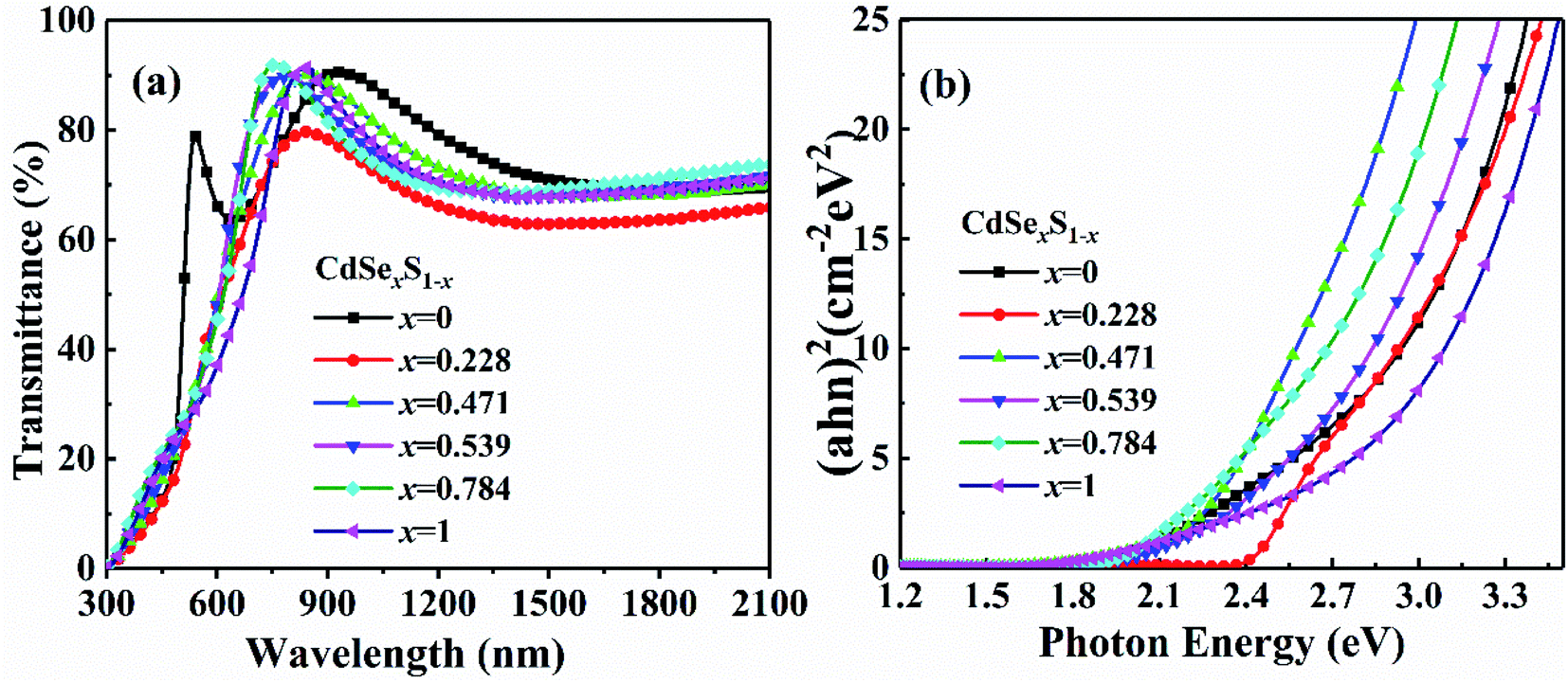
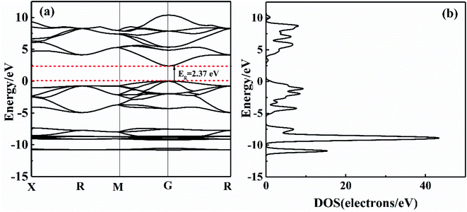
The calculated and experimental band gaps of CdSexS1−x are shown in Fig. 5. The CdSexS1−x films was fabricated by magnetron sputtering on a silica glass substrate at room temperature which was published in another work.26 The Se concentration x was measured by X-ray fluorescence spectrometer (XRF) of RIGAKU ZSX Primus model. The transmittance spectra of CdSexS1−x film was measured by the Lambda 950 spectrophotometer of PerkinElmer, as shown in Fig. 4(a). The optical energy band gap can be calculated according to Tauc formula: (αhν)2 = A(hν − Eg), where α is the absorption coefficient, h is Planck's constant, A is a constant and Eg is the band-gap, respectively. The optical band-gap can be obtained through extrapolating (αhν)2 vs. photon energy (hν). The energy band gaps of CdSexS1−x are as shown in Fig. 3(b). The Tauc plot shows that the band gap decreases, as expected, with increasing Se concentration.
 |
| | Fig. 4 (a) Optical transmittance spectra and (b) band-gap of CdSexS1−x films. | |
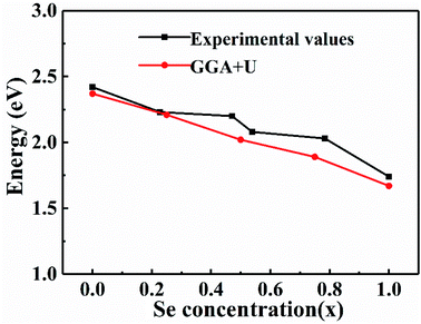 |
| | Fig. 5 The band gaps of CdSexS1−x alloy as a function of Se concentration x. | |
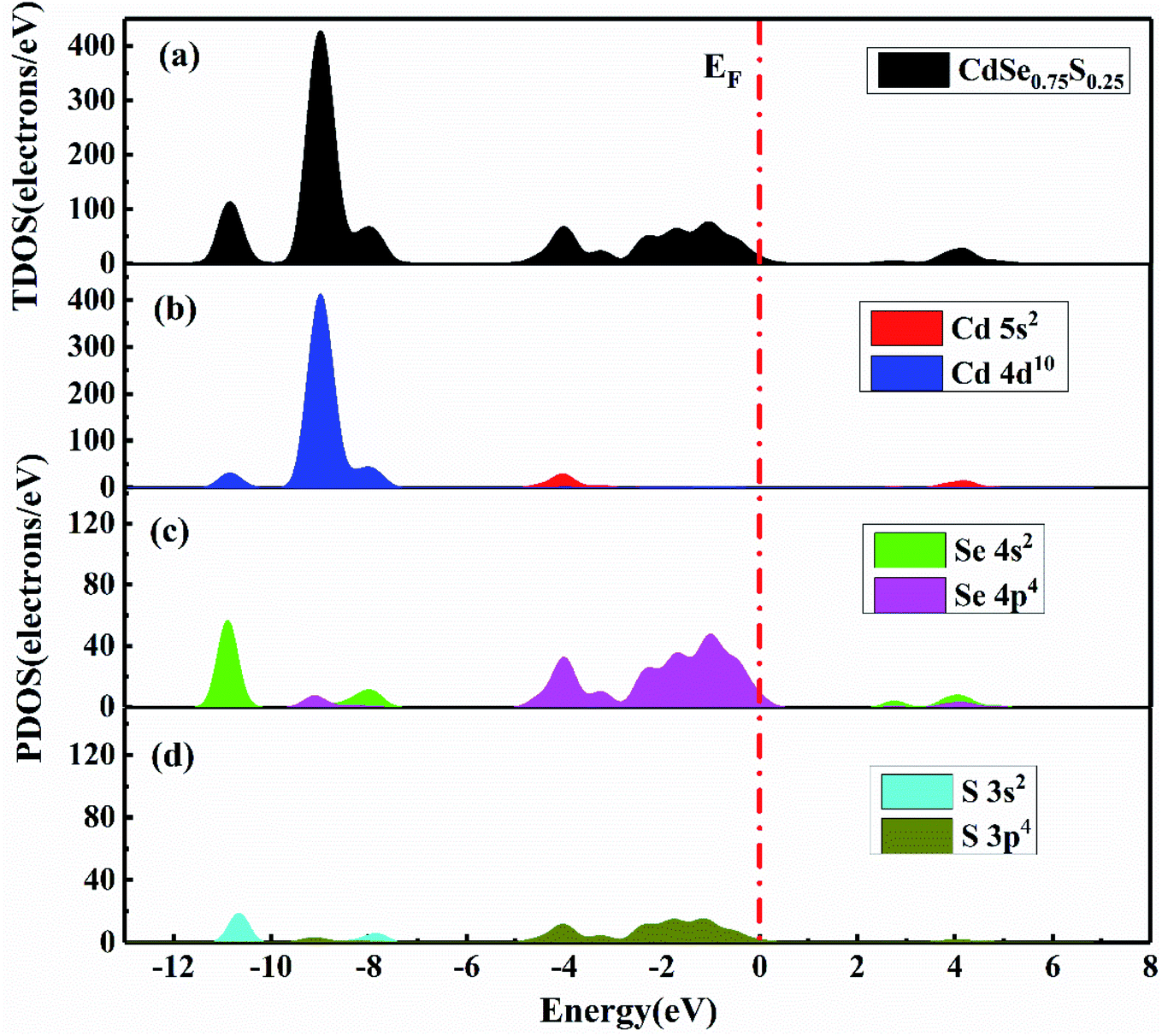
As shown in Fig. 5, both the experimental and calculation results have demonstrated that the band gaps of CdSexS1−x decrease with Se concentration among different doping cases. Fig. 6 presents the TDOS and partial density of state (PDOS) of CdSexS1−x (x = 0.75). Cd-4d105s2, S-3s23p4, Se-4s24p4 are treated as valence states. The EVBM and ECBM near the Fermi level are mainly formed by the interaction between the bonding valence band orbital of Se-4p and Se-4s. Fig. 6(c) indicates that Se-4p states tend to the direction of high energy, resulting in the decrease of CdSexS1−x band gap with the increase of Se concentration.
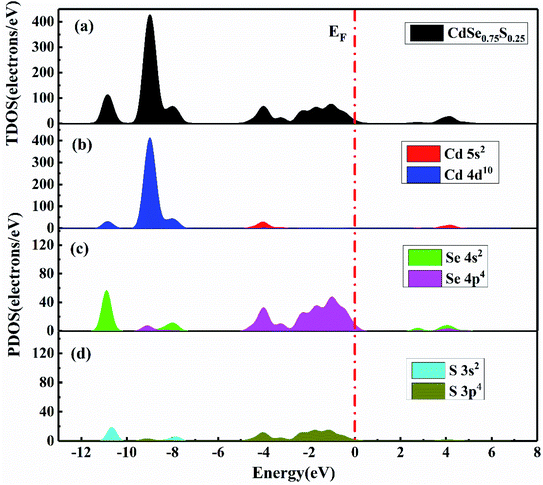 |
| | Fig. 6 Calculated (a) total and (b–d) partial densities of state of the ternary alloy CdSe0.75S0.25. | |
3.2 The performances of CdSexS1−x/CdTe solar cells
3.2.1 The performances of CdSexS1−x/CdTe solar cells. The illuminated current density–voltage and the external quantum efficiency (EQE) for CdTe solar cells with 100 nm CdSexS1−x are shown in Fig. 7(a) and (b). Here, all SCAPS simulation have been performed under standard illumination conditions, 100 mW cm−2 AM 1.5 spectrum at 300 K. Table 4 shows the detailed performance parameters of the CdTe solar cells for different Se concentrations. The shunt resistance (Rsh) and series resistance (Rs) are estimated from the J–V curves by fitting the slope of the current density near the short circuit and open circuit voltage points, respectively.27
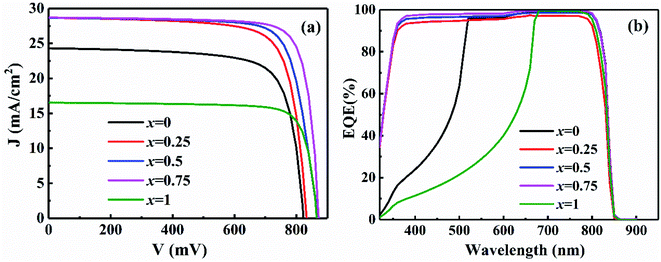 |
| | Fig. 7 (a) J–V curves and (b) external quantum efficiency of CdSexS1−x/CdTe solar cells. | |
Table 4 The performance parameters of CdSexS1−x/CdTe solar cells by SCAPS
| Parameters |
CdSexS1−x |
| x = 0 |
x = 0.25 |
x = 0.5 |
x = 0.75 |
x = 1 |
| VOC/mV |
821 |
834 |
871 |
872 |
866 |
| JSC/mA cm−2 |
24.34 |
28.22 |
28.66 |
28.69 |
16.52 |
| FF (%) |
75.38 |
76.38 |
77.09 |
81.19 |
81.15 |
| η (%) |
15.06 |
18.25 |
19.27 |
20.34 |
11.62 |
| Rs (Ω cm2) |
4.6 |
4.2 |
3.9 |
3.7 |
3.5 |
| Rsh (Ω cm2) |
812 |
1156 |
1298 |
1376 |
1331 |
The simulation efficiency achieved for baseline model CdS/CdTe control is 15.06% as shown in Table 4, which is close to the results of our recent experiment and other works.9,13,15 It is reasonable that the property parameters and defect settings for each layer are close to that in the actual device performance. Table 4 shows that the JSC of CdTe solar cells increased to the maximum value of 28.69 mA cm−2 when Se concentration x is 0.75. Furthermore, the fill factor (FF) has a substantial increase, close to the maximum of 81.19% when Se contents is 0.75. One may notice that, as shown in Table 4, with the increased concentration of Se from x = 0 to x = 1, the series resistance of device decreased from 4.6 Ω cm2 to 3.5 Ω cm2. On the contrary, the shunt resistance increased from 812 Ω cm2 to 1376 Ω cm2 with x varied from 0 to 0.75, followed by a decrease with further increased Se content.
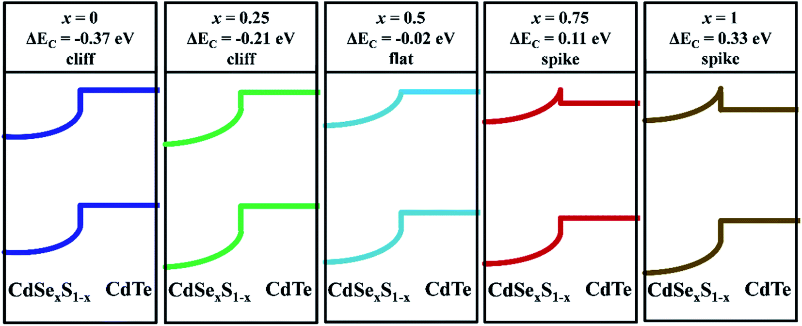
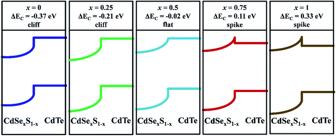
As discussed above, the main contribution of the CdTe efficiency improvement was attributed to the increase of JSC and FF. Fig. 7(b) shows that the short-wavelength EQE response of CdTe solar cells was obviously increased due to CdSexS1−x replacing CdS window layer. Furthermore, the ability of the photon absorption and carriers separation in devices is closely related to the conduction band offset (CBO) of the window/CdTe layers. The improvement of JSC can be attributed to a decrease of recombination at the CdSexS1−x/CdTe interface due to the appropriate CBO. In order to further analyze the effects of intrinsic causes and mechanisms on the CdTe device performance, the band diagrams of CdSexS1−x/CdTe layers are shown in Fig. 8.
 |
| | Fig. 8 Schematic band diagram of CdSexS1−x/CdTe solar cells under equilibrium. | |
3.2.2 The energy band alignment of CdSexS1−x/CdTe interface. Based on the energy band parameters of CdSexS1−x as labeled in Table 4 and CdTe energy band parameters9 (χCdTe = 4.5 eV, Eg = 1.5 eV), Fig. 8 shows the band diagram of CdSexS1−x and CdTe layers with different Se contents. A barrier spike (ΔEC) is formed at the CdSexS1−x/CdTe interface due to the difference of electron affinity (χ) between CdSexS1−x and CdTe layers. The specific values could be obtained from the formula ΔEC = χCdSexS1−x − χCdTe. As shown in Table 5, when the Se concentration x increases from 0 to 1, the corresponding ΔEC gradually increases from −0.37 eV (x = 0) to 0.33 eV (x = 1). It indicates that the CBO of CdSexS1−x/CdTe layers can be controlled by changing the Se contents.
Table 5 The energy band parameters of CdSexS1-x with different x contention
| x |
0 |
0.25 |
0.5 |
0.75 |
1 |
| Eg/eV |
2.37 |
2.21 |
2.02 |
1.89 |
1.67 |
| χ/eV |
4.13 |
4.29 |
4.48 |
4.61 |
4.83 |
| ΔEc/eV |
−0.37 |
−0.21 |
−0.02 |
0.11 |
0.33 |
Fig. 8(a)–(c) show the band diagrams of the CdTe solar cells when the ECBM of the window layers CdSexS1−x is below that of CdTe. A cliff is formed at the CdSexS1−x/CdTe interface because the χ of CdSexS1−x is smaller than that of CdTe. At forward bias, the cliff acts as a barrier against injected electrons from CdSexS1−x. The recombination between majority carriers via defects at the CdSexS1−x/CdTe interface thus increase drastically, resulting in a decrease of JSC.
Fig. 8(d) and (e) show band diagrams of the CdTe solar cells when the conduction band minimum of the window layers CdSexS1−x is above that of CdTe. In contrast to the band diagrams shown in Fig. 8(a)–(c), a spike is formed at the CdSexS1−x/CdTe interface. The VOC, JSC and FF all reached their peaks due to the appropriate CBO when the spike is about 0.11 eV (x = 0.75). However, if the barrier spike is too high as shown in Fig. 8(e), which acts as the barrier against photogenerated electrons in the CdTe layer and prevents the photogenerated electrons to window layer. The variation of CBO is consistent with the effect of Rs and Rsh. Therefore, an appropriate spike is necessary at the window/CdTe interface to depress the majority carrier recombination via the interface defects while not impeding electrons transportation to window layer. This is accordance with other works.28–30
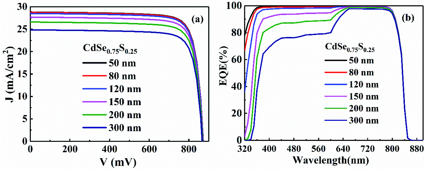
3.2.3 Effect of CdSexS1−x (x = 0.75) thickness on CdTe solar cells performances. To further optimize the window layer, the dependence of the CdTe solar cells on the thickness of CdSexS1−x (x = 0.75) film was investigated. The current–voltage (J–V) curves and the EQE of CdTe solar cells with 50–300 nm CdSe0.75S0.25 were illustrated in Fig. 9. Table 6 shows the detail performance parameters of the champion cells for CdSexS1−x (x = 0.75). The JSC decreases significantly from 28.73 mA cm−2 to 24.84 mA cm−2 while the thickness of CdSe0.75S0.25 increases from 80 nm to 300 nm. The corresponding conversion efficiency (η) of CdTe solar cells decreases from ∼20% to ∼17%. The results indicate that the window layer absorbs more short-wave photons with increasing thickness, which results in more loss of photoelectric current. Fig. 9(b) shows that the EQE at short wavelength 320–650 nm decrease drastically when the CdSe0.75S0.25 thickness greater than 120 nm, which has the same change with the JSC of CdTe solar cells. As shown in Table 6, the VOC and FF have no obvious change with the CdSe0.75S0.25 thickness, which is due to the same CBO. Furthermore, CdSe0.75S0.25 window layers with the thickness from 50 nm to 120 nm lead to the similar device performances. This result suggests that the effect of CdSe0.75S0.25 thickness is not significant in the range of <120 nm. Therefore, in the practical device fabrication, good performance could be obtained if the thickness of CdSe0.75S0.25 window layer could be controlled at 50–120 nm.
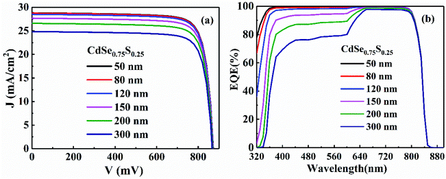 |
| | Fig. 9 (a) J–V curves and (b) external quantum efficiency of CdTe solar cell with different thickness of CdSexS1−x. | |
Table 6 Dependence of cell performance parameters on different thickness of CdSe0.75S0.25
| Thickness/nm |
50 |
80 |
120 |
150 |
200 |
300 |
| VOC/mV |
873 |
872 |
871 |
871 |
870 |
868 |
| JSC/mA cm−2 |
28.81 |
28.73 |
28.50 |
27.68 |
26.59 |
24.84 |
| FF% |
81.28 |
81.21 |
81.19 |
81.13 |
81.05 |
80.19 |
| η/% |
20.45 |
20.37 |
20.19 |
19.58 |
18.76 |
17.45 |
4. Conclusion
The crystal structure and electronic structures of the CdSexS1−x ternary have been studied by CASTEP. The band gap of CdSexS1−x decreases from 2.37 eV to 1.67 eV as the content of Se increasing. The simulation results indicate that the conversion efficiency of CdTe solar cell reaches 20.34% because the recombination decreases obviously due to the appropriate CBO about 0.11 eV at CdSexS1−x/CdTe interface and an optimal value FF when Se concentration is 0.75. The effects of CdSexS1−x thickness is mainly on the JSC of CdTe solar cells. Our insights into the device performance indicate that the performance of CdTe solar cells could be optimized by using a 50–120 nm-thick CdSexS1−x window layer with dopant concentrations for Se of 0.75. These results suggest that the positive effect of CdS/CdSe composite window layer roots in the appropriate CBO between CdSe0.75S0.25 and CdTe. These simulation results will become an integral part of the design rule for window layer and provide a theoretical guidance for the fabrication of highly efficient CdTe solar cells.
Conflicts of interest
There are no conflicts of interest to declare.
Acknowledgements
This work was supported by the National High Technology Research and Development Program of China (grant number 2015AA050610) and the Natural Science Foundation Project of Chengdu Textile College (Grant No. X18009). The authors acknowledge the use of SCAPS program developed by Prof. Burgelman's group of the University of Ghent, Belgium. In addition, the authors would like to thank National Supercomputing Center in Shenzhen for providing simulation calculation support.
References
- M. A. Green, K. Emery, Y. Hishikawa, W. Warta and E. D. Dunlop, Prog. Photovolt., 2012, 20, 606–614 CrossRef.
- M. A. Green, Y. Hishikawa, E. D. Dunlop, D. H. Levi, J. Hohl-Ebinger, M. Yoshita and A. W. Y. Ho-Baillie, Prog. Photovolt., 2019, 27, 3–12 CrossRef.
- N. R. Paudel and Y. Yan, Appl. Phys. Lett., 2014, 105(18), 183510 CrossRef.
- S. Marjani, S. Khosroabadi and M. Sabaghi, Opt. Photon. J., 2016, 06, 15–23 CrossRef CAS.
- H. Alrashidi, A. Ghosh, W. Issa, N. Sellami, T. K. Mallick and S. Sundaram, Mater. Lett., 2019, 237, 332–335 CrossRef CAS.
- S.-H. Wei, S. B. Zhang and A. Zunger, J. Appl. Phys., 2000, 87, 1304–1311 CrossRef CAS.
- J. M. Kephart, J. W. McCamy, Z. Ma, A. Ganjoo, F. M. Alamgir and W. S. Sampath, Sol. Energy Mater. Sol. Cells, 2016, 157, 266–275 CrossRef CAS.
- M. A. K. Sheikh, R. Abdur, S. Singh, J.-H. Kim, K.-S. Min, J. Kim and J. Lee, Electron. Mater. Lett., 2018, 14, 700–711 CrossRef CAS.
- H. Xu, R. Sheng-Qiang, L. Chun-Xiu, W. Li-Li, Z. Jing-Quan and D. Zheng, J. Inorg. Mater., 2018, 33, 635 CrossRef.
- T. Wang, S. Ren, C. Li, W. Li, C. Liu, J. Zhang, L. Wu, B. Li and G. Zeng, Solar Energy, 2018, 164, 180–186 CrossRef CAS.
- S. Mahato, N. Shakti and A. K. Kar, Mater. Sci. Semicond. Process., 2015, 39, 742–747 CrossRef CAS.
- T. Kacsich and K.-P. Lieb, Thin Solid Films, 1994, 245, 4–6 CrossRef CAS.
- C. Li, F. Wang, Y. Chen, L. Wu, J. Zhang, W. Li, X. He, B. Li and L. Feng, Mater. Sci. Semicond. Process., 2018, 83, 89–95 CrossRef CAS.
- M. Burgelman, P. Nollet and S. Degrave, Thin Solid Films, 2000, 361–362, 527–532 CrossRef CAS.
- J. Pettersson, C. Platzer-Björkman, U. Zimmermann and M. Edoff, Thin Solid Films, 2011, 519, 7476–7480 CrossRef CAS.
- T. Minemoto, T. Matsui, H. Takakura, Y. Hamakawa, T. Negami, Y. Hashimoto, T. Uenoyama and M. Kitagawa, Sol. Energy Mater. Sol. Cells, 2001, 67, 83–88 CrossRef CAS.
- M. Patel and A. Ray, Phys. B, 2012, 407, 4391–4397 CrossRef CAS.
- M. Olopade, O. Oyebola and B. S. Adeleke, Adv. Appl. Sci. Res., 2012, 3, 3396–3400 CAS.
- C.-H. Huang and W.-J. Chuang, Vacuum, 2015, 118, 32–37 CrossRef CAS.
- A. J. Clayton, V. Di Carlo, S. J. C. Irvine, G. Kartopu, V. Barrioz and D. A. Lamb, Mater. Res. Innovations, 2014, 18, 505–508 CrossRef CAS.
- Z. Jingquan, Study on CdTe and Related Compound Polycrystalline Thin Films as well as CdTe Solar Cell, Doctor thesis, Sichuan University, Chengdu, 2002 Search PubMed.
- S. J. Clark, M. D. Segall, C. J. Pickard, P. J. Hasnip, M. I. J. Probert, K. Refson and M. C. Payne, Z. Kristallogr. - Cryst. Mater., 2005, 220, 567–570 CrossRef CAS.
- Y. Wu, G. Chen, Y. Zhu, W.-J. Yin, Y. Yan, M. Al-Jassim and S. J. Pennycook, Comput. Mater. Sci., 2015, 98, 18–23 CrossRef CAS.
- E. Valcheva, G. Yordanov, H. Yoshimura, T. Ivanov and K. Kirilov, Colloids Surf., A, 2014, 461, 158–166 CrossRef CAS.
- J. Heyd, J. E. Peralta, G. E. Scuseria and R. L. Martin, J. Chem. Phys., 2005, 123(17), 174101 CrossRef.
- C. Li, A. Wang, L. Wu, X. He, J. Zhang, X. Hao and L. Feng, J. Mater. Sci.: Mater. Electron., 2020, 31, 21455–21466 CrossRef CAS.
- J. Han, C. Spanheimer, G. Haindl, G. Fu, V. Krishnakumar, J. Schaffner, C. Fan, K. Zhao, A. Klein and W. Jaegermann, Sol. Energy Mater. Sol. Cells, 2011, 95, 816–820 CrossRef CAS.
- T. Song, A. Kanevce and J. R. Sites, J. Appl. Phys., 2016, 119(23), 233104 CrossRef.
- J. Sites and J. Pan, Thin Solid Films, 2007, 515, 6099–6102 CrossRef CAS.
- T. Ablekim, E. Colegrove and W. K. Metzger, ACS Appl. Energy Mater., 2018, 1, 5135–5139 CAS.
|
| This journal is © The Royal Society of Chemistry 2022 |
Click here to see how this site uses Cookies. View our privacy policy here. 
 Open Access Article
 This Open Access Article is licensed under a Creative Commons Attribution-Non Commercial 3.0 Unported Licence
 d,
Jingquan Zhangb,
Lianghuan Fengb,
Peng Tang
d,
Jingquan Zhangb,
Lianghuan Fengb,
Peng Tang

 are the effective masses of electrons/holes, h is Planck's constant and k is the Boltzmann constant. Thermal velocities for electrons (ve) and holes (vp) are obtained from the eqn (2):15

 is electron current density,
 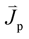 is hole current density, R and G represent the recombination and generation rate of electron hole pairs, respectively. By setting the parameters of material and the corresponding boundary conditions, SCAPS solves the above equations by numerical calculation, and obtains the related characteristics of the solar cells.