
 Open Access Article
 This Open Access Article is licensed under a Creative Commons Attribution-Non Commercial 3.0 Unported Licence
High performance of CH3NH3PbCl3 perovskite single crystal photodetector with a large active area using asymmetrical Schottky interdigital contacts†
Ji Yua,
Jie Zheng a,
Ning Tian*a,
Lin Li*b,
Yanmei Qua,
Yongtao Huanga,
Yinxian Luoa and
Wenzhu Tana
a,
Ning Tian*a,
Lin Li*b,
Yanmei Qua,
Yongtao Huanga,
Yinxian Luoa and
Wenzhu Tana
aCollege of Physics Science and Technology, Shenyang Normal University, Shenyang 110034, China. E-mail: tiann08@synu.edu.cn
bKey Laboratory for Photonic and Electronic Bandgap Materials Ministry of Education, School of Physics and Electronic Engineering, Harbin Normal University, Harbin 150025, China. E-mail: physics_lin@hotmail.com
First published on 18th August 2022
Abstract
Due to the limited electrode structure types of current CH3NH3PbCl3 perovskite single crystal photodetectors, these devices either have good performance but small active area or have large active area but poor performance, which greatly limits their applications. To realize a high performance of a CH3NH3PbCl3 perovskite single crystal photodetector with a large active area, a CH3NH3PbCl3 single crystal photodetector with asymmetrical Schottky interdigital contacts originating from planar interdigital Au–Ag electrodes was fabricated in this work. The device not only had a large active area (around 8 mm2) but also showed excellent photoelectric performance due to its built-in electric field. The responsivity of the device can reach 5.8 mA W−1 at 0 V and 0.24 A W−1 at 30 V reverse voltage. The response time of the device can reach 317 μs (rise)/6.82 ms (decay) at 0 V and 100 μs (rise)/2 ms (decay) at 30 V reverse voltage. The above results demonstrate that this study will provide an effective method for realizing high performance of a CH3NH3PbCl3 perovskite single crystal photodetector with a large active area.
Introduction
Organic–inorganic hybrid perovskites have been considered to be promising for future optoelectronic applications due to many of their excellent properties including easy preparation, low trap-state density, high carrier mobility, large light absorption coefficient, long carrier diffusion length, and tunable direct bandgap. Significant progress has been achieved in organic-inorganic hybrid perovskite based ultraviolet (UV) photodetectors.1–5 For example, Thi My Huyen Nguyen et al. reported that a photodetector based on (FAPbI3)1−x(MAPbBr3)x perovskite presented excellent performance with a fast response speed (trise = 82 ms, tfall = 64 ms) and a high detectivity of 7.21 × 10¹⁰ Jones at zero bias under 254 nm UV illumination, along with superior mechanical flexibility at various bending angles.1 Lian Ji et al. reported that a self-driven visible-blind UV photodetector based on CsPbCl3 perovskite film showed outstanding properties with a high responsivity of 118 mA W−1, a high detectivity of 6.62 × 10¹² Jones, and a fast rise/fall response time of 120/820 ns.2 Dali Shao et al. reported that Cs2SnI6/ZnO structured UV-vis dual-band photodetector exhibited good performance of a high detectivity in UV (1.39 × 10¹² jones), a fast response speed on the order of milliseconds.3 Thi My Huyen Nguyen et al. reported that a self-powered deep UV photodetector based on (FAPbI3)0.97(MAPbBr3)0.03 perovskite film showed a high responsivity of 52.68 mA W−1, a good detectivity of 4.65 × 10¹¹ Jones, and an outstanding on/off photocurrent ratio of more than 103 under 254 nm UV illumination without an external bias.4 Sheng Wang et al. reported that an UV photodetector based on BA2PbBr4 (BA = CH3CH2CH2CH2NH3+) single crystal film exhibited a detectivity of ∼1012 Jones and a fast rise/decay response time of 9.7/8.8 ms.5 Among the organic-inorganic hybrid perovskites, CH3NH3PbCl3 perovskite single crystal is regarded as an attractive candidate for UV detection due to its large direct bandgap of ∼2.85 eV.6–13 At present, some progress has been made in the research of CH3NH3PbCl3 single crystal photodetectors.8–13 For example, Hye Ri Jung et al. reported that an Ag/TiO2/MAPbCl3/TiO2/Ag structured photodetector presented a responsivity of 0.004 A W−1 and a detectivity of 1.05 × 10¹⁰ Jones at 430 nm under 2 V bias voltage.8 Jingda Zhao et al. reported that a n−–n+ photo-diodes based on CH3NH3PbCl3 single crystal exhibited a responsivity of 404.7 mA W−1, and a detectivity of 4.87 × 10¹¹ Jones at 20V.9 Giacomo Maculan et al. reported that Pt/CH3NH3PbCl3 single crystal/Ti/Au vertical structured visible-blind UV-photodetector was fabricated.10 The active area of the device was about 4 mm2. At 15 V, the responsivity of the device was about 46.9 mA W−1 under illumination with 365 nm UV light. For the response speed of the device, the rise time was 24 ms and the decay time was 62 ms. Zhishuai Yuan et al. reported that the Pt/CH3NH3PbCl3 single crystal/Pt metal–semiconductor-metal (MSM) structured photodetector was fabricated.11 The active area of the device was 0.01 mm2. At 3 V, the device showed ultra-high responsivity of 7.97A W−1, and the rise time of 1.27 ms and fall time of 1.84 ms under the illumination light of 350 nm. Zhen Cheng et al. reported that the Au/CH3NH3PbCl3 single crystal/Au MSM structured photodetector was fabricated.12 The active area of the device was 0.09 mm2. The device showed the peak responsivity of 3.73 A W−1 in the wavelength of 415 nm at 30 V and an ultrafast response speed with a rise time of 130 ns at 15 V under 365 nm pulsed laser. Yan Chen et al. reported that the tetragonal phase CH3NH3PbCl3 single crystal photodetector with the interdigital Au electrodes was fabricated.13 The active area of the device was 0.2 mm2. The responsivity of the device can reach 27.7 μA W−1 at 3 V under 395 nm. The rise time and decay time of the device were 30 ms and 0.3 s, respectively.Although some achievements have been made in the research of CH3NH3PbCl3 single crystal photodetectors, due to the limited electrode structure types of current CH3NH3PbCl3 perovskite single crystal photodetectors, these devices either have good performance but small active area or have large active area but poor performance, which greatly limits their applications. The planar asymmetrical Schottky interdigital structure is an ideal electrode structure of photodetector, which can not only ensure the large active area, but also realize the high sensitivity and fast response due to its built-in electric field.14–16 However, to our knowledge, there are no reports on the CH3NH3PbCl3 perovskite single crystal photodetectors with asymmetrical Schottky interdigital electrodes. In this work, to realize the high performance of CH3NH3PbCl3 perovskite single crystal photodetector with a large active area, a CH3NH3PbCl3 single crystal photodetector with asymmetrical Schottky interdigital contacts originated from planar interdigital Au–Ag electrodes was fabricated in this work. The device not only had a large active area (around 8 mm2) but also showed excellent photoelectric performance.
Experimental
The CH3NH3PbCl3 single crystals were prepared by the inverse temperature crystallization method, which has been reported in detail elsewhere.13 An equimolar mixture of CH3NH3Cl and PbCl2 was dissolved in DMSO-DMF (1![[thin space (1/6-em)]](https://www.rsc.org/images/entities/char_2009.gif) :1 by volume) at room temperature to get a homogenous solution. The solution was filtered using a PTFE filter with 0.45 mm pore size. The filtrate was placed in a crystallizing dish and then was kept in an oil bath heated from 45 °C to 60 °C at the rate of 0.3 °C h−1. CH3NH3PbCl3 single crystals with sizes of ∼1 cm were attained. The Au and Ag electrodes of the photodetector based on CH3NH3PbCl3 single crystal were fabricated via thermal evaporation through shadow masks. Fig. 1 shows the preparation process diagram of the Au/CH3NH3PbCl3 single crystal/Ag structured photodetector. Firstly, Au electrodes are evaporated on the surface of the single crystal through a comb-shaped shadow mask. Au electrodes have five fingers with the length of 4.45 mm and width of 50 μm, and the spacing of Au electrodes is 450 μm. Then, Ag electrodes are fabricated on the surface of the single crystal by the same method as Au electrodes. The parameters of Ag electrodes are the same as those of Au electrodes. Thus, planar interdigital Au–Ag electrodes are formed on the surface of the single crystal. The spacing of the Au–Ag interelectrode is about 200 μm. The active area of the device is around 8 mm2, which is one of the largest active area for reported CH3NH3PbCl3 single crystal photodetectors.8–13
:1 by volume) at room temperature to get a homogenous solution. The solution was filtered using a PTFE filter with 0.45 mm pore size. The filtrate was placed in a crystallizing dish and then was kept in an oil bath heated from 45 °C to 60 °C at the rate of 0.3 °C h−1. CH3NH3PbCl3 single crystals with sizes of ∼1 cm were attained. The Au and Ag electrodes of the photodetector based on CH3NH3PbCl3 single crystal were fabricated via thermal evaporation through shadow masks. Fig. 1 shows the preparation process diagram of the Au/CH3NH3PbCl3 single crystal/Ag structured photodetector. Firstly, Au electrodes are evaporated on the surface of the single crystal through a comb-shaped shadow mask. Au electrodes have five fingers with the length of 4.45 mm and width of 50 μm, and the spacing of Au electrodes is 450 μm. Then, Ag electrodes are fabricated on the surface of the single crystal by the same method as Au electrodes. The parameters of Ag electrodes are the same as those of Au electrodes. Thus, planar interdigital Au–Ag electrodes are formed on the surface of the single crystal. The spacing of the Au–Ag interelectrode is about 200 μm. The active area of the device is around 8 mm2, which is one of the largest active area for reported CH3NH3PbCl3 single crystal photodetectors.8–13
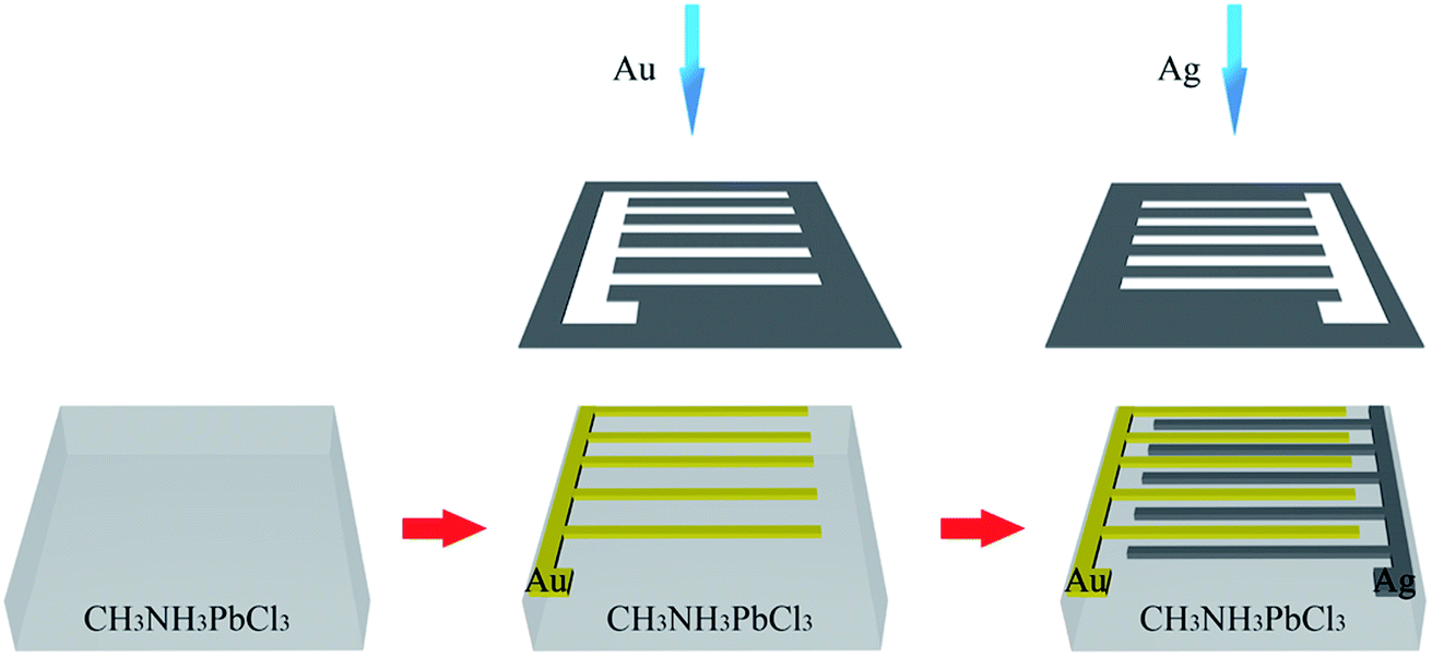 | ||
| Fig. 1 Preparation process diagram of the Au/CH3NH3PbCl3 single crystal/Ag structured photodetector. | ||
The crystal structure of the CH3NH3PbCl3 single crystal and its powder was characterized by X-ray diffraction (XRD) (Rigaku-D-Max Ra system, with Cu Ka radiation operated at 12 kW). The surface morphology of the CH3NH3PbCl3 single crystal was characterized by SU8220 scanning electron microscope (SEM). The absorption spectra of the CH3NH3PbCl3 single crystal were determined by UV-3101PC spectrophotometer. The current–voltage (I–V) curves of the photodetector were obtained from a computerized Keithley 2400 SourceMeter. The response spectra and photocurrent–time (I–t) curves of the device were measured by a lock-in amplifier, where the light source is a Xe lamp (150 W) with a monochromator and a chopper with a frequency of 500 Hz. The response time of the device was recorded by an oscilloscope under the excitation of a 355 nm pulsed laser.
Results and discussion
To study the crystal structures of CH3NH3PbCl3 single crystal and its powder, X-ray diffraction (XRD) characterization is carried out, which is shown in Fig. 2(a). Pure single phase of cubic MAPbCl3 perovskite can be noted from the XRD pattern of CH3NH3PbCl3 powder obtained by grinding single crystal. Lattice constant is obtained by Rietveld refinement of the powder XRD data, which is shown in Fig. 2(b). The lattice constant is 0.5689 nm. Because the single crystal has the characteristic of preferential growth of crystal planes, only three sharp peaks corresponding to (100), (200), and (400) crystal planes can be found in the single crystal XRD pattern, which shows that the single crystal is preferably oriented in the (100) direction. The inset of Fig. 2(c) shows the photograph of the single crystal with a cuboid shape and the dimension of 10 mm × 9 mm × 4 mm. The SEM of the single crystal is shown in Fig. 2(c). It can be noted that its surface is very flat and uniform. The absorption spectrum of the single crystal is displayed in Fig. 2(d). It can be seen that the single crystal exhibits the intense absorption in the 300–435 nm wavelength region, and has a sharp absorption edge located at 435 nm. Based on this, the bandgap of the single crystal is calculated as 2.85 eV, which is suitable for UV detection.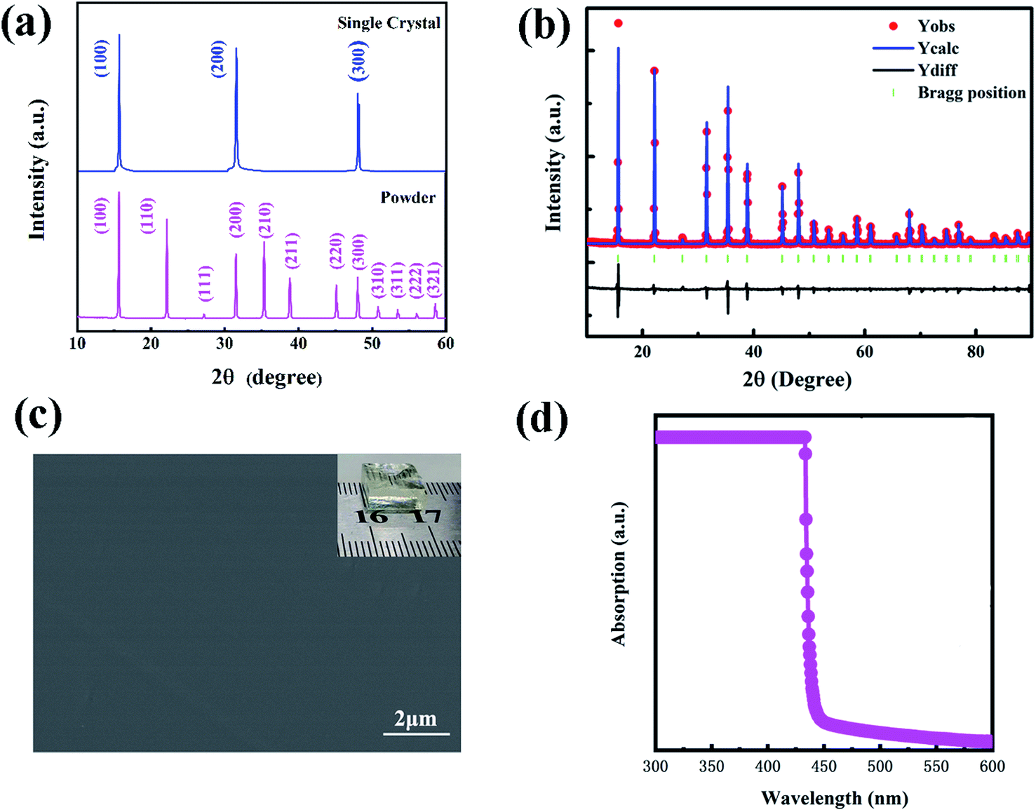 | ||
| Fig. 2 (a) X-ray diffraction patterns of CH3NH3PbCl3 single crystal and its powder. (b) Rietveld refinement of the powder XRD data. (c) SEM of the single crystal. Inset: photograph of the CH3NH3PbCl3 single crystal. (d) Absorption spectrum of CH3NH3PbCl3 single crystal. | ||
Fig. 3(a) shows the current–voltage (I–V) curve of the Au/CH3NH3PbCl3 single crystal/Ag structured photodetector measured in the dark under forward and reverse bias. Note that the reverse bias of the device refers to the Au electrode as the anode and the Ag electrode as the cathode, and the forward bias of the device refers to the Au electrode as the cathode and the Ag electrode as the anode. Obviously, the device shows the asymmetrical I–V behavior under forward and reverse bias, which is caused by the Au–Ag electrodes of the device. The I–V curve of the CH3NH3PbCl3 single crystal photodetector with symmetrical Au electrodes in dark is shown in the Fig. S1.† It can be noted that the device shows the symmetrical I–V behavior under forward and reverse bias, which is caused by the symmetrical Au electrodes of the device. Energy band diagram for the device with Au–Ag electrodes is shown in Fig. 3(b). The valence band maxima (VBM) of CH3NH3PbCl3 single crystal is reported to be −5.82 eV.10 Based on its bandgap of 2.85 eV in our case, its conduction band minimum (CBM) can be calculated to be −2.97 eV. Schottky contacts are formed at the interface between the CH3NH3PbCl3 single crystal and the metal electrodes. Schottky barrier heights are primarily determined by the work function of metals and the electron affinity of the CH3NH3PbCl3 single crystal. A high Schottky barrier is formed at the interface of Ag (the work function of −4.26 eV)17 and the single crystal, and a low Schottky barrier is formed at the interface of Au (the work function of −5.1 eV)15 and the single crystal. So the asymmetrical Schottky interdigital contacts are generated by Au–Ag electrodes of the device, which leads to the asymmetrical I–V behavior of the device under forward and reverse bias. A built-in electric field from Au to Ag is formed in the device, which allows the device to collect photogenerated carriers without any external bias. Responsivity (R) of the photodetectors is calculated by the following expression:10
 | (1) |
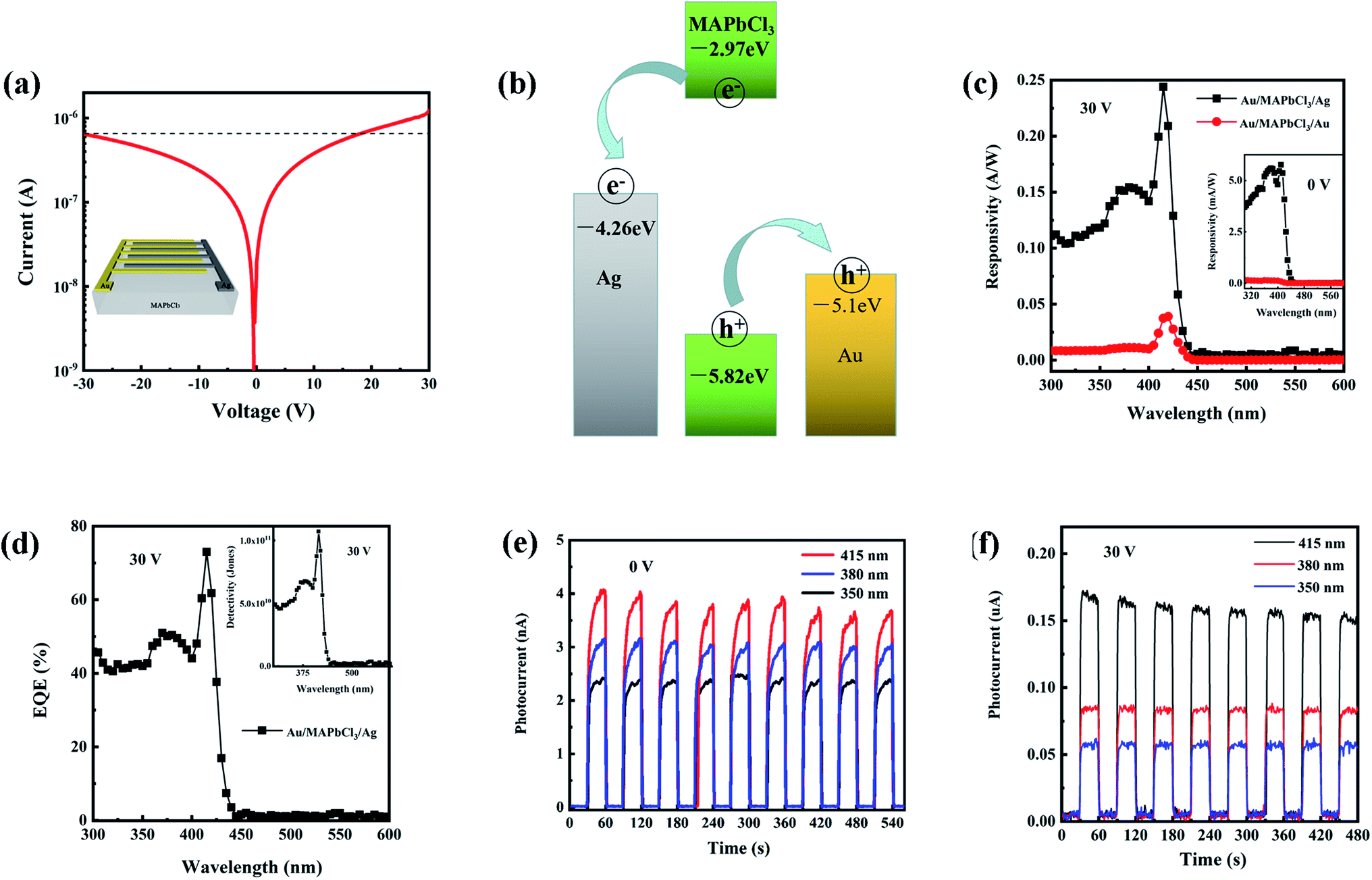 | ||
| Fig. 3 (a) Current–voltage (I–V) curve of the device measured in dark under forward and reverse bias, with the inset showing a schematic diagram of the device structure. (b) Energy band diagram for the device. (c) Photoresponse spectra of the devices with Au–Ag electrodes at 30 V reverse bias and with symmetrical Au electrodes at 30 V. Inset: the photoresponse spectra of the above two structured devices at 0 V. (d) External quantum efficiency of the device at 30 V. Inset: detectivity of the device at 30 V. Short-term stability of the device at 0 V (e) and 30 V reverse bias (f). | ||
The photoresponse spectrum of the device at 0 V is shown in the inset of Fig. 3(c). It can be noted that the device shows the maximum responsivity of 5.8 mA W−1 at 410 nm at 0 V. As a comparison, the spectral response of the CH3NH3PbCl3 single crystal photodetector with symmetrical Au electrodes is also measured. The parameters of the symmetrical interdigital Au electrodes are same as those of the asymmetrical interdigital Au–Ag electrodes. There is almost no response for the device with symmetrical Au electrodes at 0 V. The results demonstrate that the built-in electric field is the key to realize self-powered photodetector. The photoresponse spectrum of the photodetector with Au–Ag electrodes at 30 V reverse bias is shown in Fig. 3(c). The device exhibits the broad photoresponse in the 300–420 nm wavelength region, and the cutoff wavelength of the photoresponse locates at around 420 nm, which indicates that the device is very suitable for UV detection. The responsivity of the device can reach 0.24 A W−1 at 415 nm, which is 7 times that of the device with symmetrical Au electrodes under the same bias. The above results indicates that the built-in electric field can improve the sensitivity of photodetector. The external quantum efficiency (EQE) of the photodetector can be determined by the following formula:12,18
 | (2) |
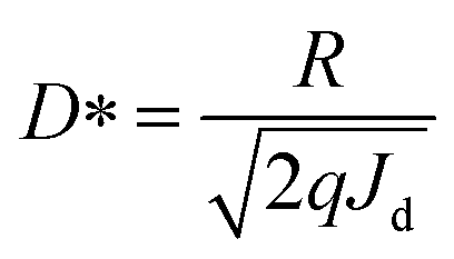 | (3) |
Response speed is an important parameter of photodetector, which can be characterized by the transient photocurrent response. Fig. 4(a) and 4(b) show the transient photocurrent response of the device with the light source of a 355 nm pulsed laser at 0 V and 30 V reverse bias, respectively. The rise and decay time is defined as the time for the photocurrent to change from 10% to 90% of its maximum value, and vice versa. The rise/decay times of the device at 0 V and 30 V reverse bias are 317 μs/6.82 ms and 100 μs/2 ms, respectively.
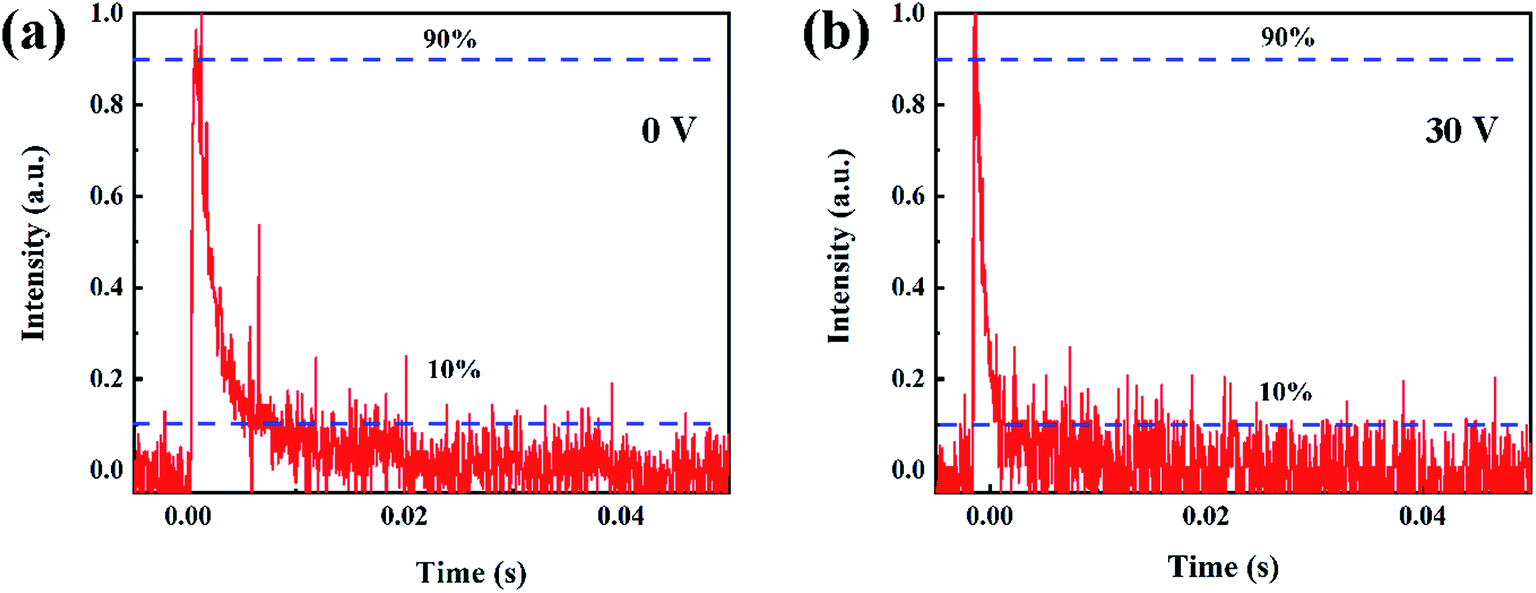 | ||
| Fig. 4 Transient photocurrent response of the device with the light source of a 355 nm pulsed laser at 0 V (a) and 30 V reverse bias (b). | ||
To evaluate the performance of the device, we compared the critical parameters of the device with the reported CH3NH3PbCl3 single crystal photodetectors, as shown in Table 1. The R, EQE, D*, response time, and active area of the device in this work are obviously better than those of ref. 10 and 13. The R, EQE, D*, and response time of the device in this work are lower than those of ref. 11 and 12. However, the area of the device in this work is larger than that of ref. 11 and 12. So high performance of CH3NH3PbCl3 perovskite single crystal photodetector with a large active area has been realized in our case.
| Photodetector structure | R (A W−1) | EQE (%) | D* (Jones) | Response time (rise time/decay time) | Active area (mm2) | Ref. |
|---|---|---|---|---|---|---|
| Pt/CH3NH3PbCl3 single crystal/Ti/Au vertical structure | 0.05 (365 nm) | NA | 1.2 × 10¹⁰ (365 nm) | 24 ms/62 ms | 4 | 10 |
| Pt/CH3NH3PbCl3 single crystal/Pt MSM structure | 7.97 (350 nm) | NA | NA | 1.27 ms/1.84 ms | 0.01 | 11 |
| Au/CH3NH3PbCl3 single crystal/Au MSM structure | 3.73 (415 nm) | 1115 (415 nm) | 9.97 × 10¹¹ (415 nm) | 130 ns/368 μs | 0.09 | 12 |
| Au/CH3NH3PbCl3 single crystal/Au planar interdigital structure | 2.77 × 10⁻⁵ (395 nm) | NA | NA | 30 ms/0.3 s | 0.2 | 13 |
| Au/CH3NH3PbCl3 single crystal/Ag planar interdigital structure | 0.24 (415 nm) | 73 (415 nm) | 1.1 ×10¹¹ (415 nm) | 100 μs/2 ms | 8 | This work |
To assess the long term stability of CH3NH3PbCl3 single crystal photodetector, the performance of the Au/CH3NH3PbCl3 single crystal/Ag structured photodetector has been tested after 6 months storage in a small round sample box under ambient conditions, which is shown in the Fig. S2.† From the Fig. S2a,† it can be noted that the responsivity of CH3NH3PbCl3 single crystal photodetector decreases significantly compared with that of the device six months ago. As can be seen from the Fig. S2b and S2c,† although the performance of the device has decreased, the device can still work stably.
Conclusions
In this work, a CH3NH3PbCl3 single crystal photodetector with asymmetrical Schottky interdigital contacts originated from planar interdigital Au–Ag electrodes was fabricated. The device not only had a large active area (around 8 mm2) but also showed excellent photoelectric performance due to its built-in electric field. The responsivity of the device can reach 5.8 mA W−1 at 0 V and 0.24 A W−1 at 30 V reverse voltage. The response time of the device can reach 317 μs (rise)/6.82 ms (decay) at 0 V and 100 μs (rise)/2 ms (decay) at 30 V. The above results indicate that high performance of CH3NH3PbCl3 perovskite single crystal photodetector with a large active area has been realized in this work.Conflicts of interest
There are no conflicts to declare.Acknowledgements
This work is supported by the National Natural Science Foundation of China (Grant no. 12074095, 11804235, 11704264), the Support Plan for Young and Middle-Aged Scientific and Technological Innovation Talents of Shenyang City (Grant no. RC200213), the Natural Science Foundation of Heilongjiang Province (Grant no. LH2019A016) and the 2020 Central Government's plan to support the Talent Training Project of the Reform and Development Fund of Local Universities (Grant no.2020YQ02).References
- T. M. H. Nguyen, S. K. Lee, S. Kim and C. W. Bark, Practical Demonstration of Deep-Ultraviolet Detection with Wearable and Self-Powered Halide Perovskite-Based Photodetector, ACS Appl. Mater. Interfaces, 2021, 13, 57609–57618 CrossRef CAS PubMed.
- L. Ji, Y. Y. Fang, Z. C. Cheng, Y. Liu, J. G. Wang, Z. H. Li, Y. C. Qian, F. Liu, W. X. Xu, Z. C. Wu, F. F. Wang, A. F. Wang, L. Wang, Y. Di, W. Huang and T. S. Qin, Ultrafast Response (<1 μs) Perovskite Ultraviolet Photodetector via Ball-Milling Pretreated Single-Source Vapor Deposition, Adv. Mater. Technol., 2022, 7, 2100392 CrossRef CAS.
- D. Shao, W. G. Zhu, G. Q. Xin, X. Q. Liu, T. M. Wang, S. F. Shi, J. Lian and S. Sawyer, High performance UV-visible dual-band photodetector based on inorganic Cs2SnI6 perovskite/ZnO heterojunction structure, J. Mater. Chem. C, 2019, 8, 1819–1825 RSC.
- T. M. H. Nguyena, S. Kima and C. W. Bark, Solution-processed and self-powered photodetector in vertical architecture using mixed-halide perovskite for highly sensitive UVC detection, J. Mater. Chem. A, 2021, 9, 1269–1276 RSC.
- S. Wang, Y. Chen, J. J. Yao, G. X. Zhao, L. Z. Li and G. F. Zou, Wafer-sized 2D perovskite single crystal thin films for UV photodetectors, J. Mater. Chem. C, 2021, 9, 6498–6506 RSC.
- Z. Zhang, L. X. Ren, H. Yan, S. J. Guo, S. H. Wang, M. Wang and K. X. Jin, Bandgap Narrowing in Bi-Doped CH3NH3PbCl3 Perovskite Single Crystals and Thin Films, J. Phys. Chem. C, 2017, 121, 17436–17441 CrossRef CAS.
- J. Liu, W. Y. Shao, Q. Xu, Y. Liu and X. P. Ouyang, Subnanosecond X(γ)-ray sensor based on CH3NH3PbCl3 perovskite single crystals, IEEE Photonics Technol. Lett., 2020, 32, 635–638 CAS.
- H. R. Jung, Y. Cho and W. Jo, UV and Visible Photodetectors of MAPbBr3 and MAPbCl3 Perovskite Single Crystals via Single Photocarrier Transport Design, Adv. Opt. Mater., 2022, 10, 2102175 CrossRef CAS.
- J. D. Zhao, X. Wang, Y. Z. Pan, Y. B. Xu, Y. W. Li, J. Chen, J. Wu, Q. Li, Z. W. Zhao, X. B. Zhang, J. Akram, B. S. Bae, H. N. Yang and W. Lei, Photo-Diodes Based on CH3NH3PbCl3 Perovskite Single Crystals by Epitaxial Growth for Ultraviolet Photo-Detection, Front. Phys., 2021, 9, 712316 CrossRef.
- G. Maculan, A. D. Sheikh, A. L. Abdelhady, M. Saidaminov, M. A. Hague, B. Murali, E. Alarousu, O. Mohammed, T. Wu and O. M. Bakr, CH3NH3PbCl3 Single Crystals: Inverse Temperature Crystallization and Visible-Blind UV-Photodetector, J. Phys. Chem. Lett., 2015, 6, 3781–3786 CrossRef CAS PubMed.
- Z. S. Yuan, W. Huang, S. T. Ma, W. Hu and W. Zhang, A High Performance Perovskite CH3NH3PbCl3 Single Crystal Photodetector: Benefiting from an Evolutionary Preparation Process, J. Mater. Chem. C, 2019, 7, 5442–5450 RSC.
- Z. Cheng, K. Liu, J. Yang, X. Chen, X. Xie, B. Li, Z. Zhang, L. Liu, C. Shan and D. Shen, High-Performance Planar-Type Ultraviolet Photodetector Based on High-Quality CH3NH3PbCl3 Perovskite Single Crystals, ACS Appl. Mater. Interfaces, 2019, 11, 34144–34150 CrossRef CAS PubMed.
- Y. Chen, X. H. Hou, S. W. Tao, X. W. Fu, H. W. Zhou, J. Yin, M. X. Wu and X. X. Z. Synthesis, Crystal Structure and Photoresponse of Tetragonal Phase CH3NH3PbCl3 Single Crystal, Chem. Commun., 2020, 56, 6404–6407 RSC.
- A. I. Nusir and M. O. Manasre, Self-Powered Near-Infrared Photodetector Based on Asymmetrical Schottky Interdigital Contacts, IEEE Electron Device Lett., 2015, 36, 1172–1175 Search PubMed.
- Z. Bai, X. Chen, X. Yan, X. Zheng, Z. Kang and Y. Zhang, Self-powered ultraviolet photodetectors based on selectively grown ZnO nanowire arrays with thermal tuning performance, Phys. Chem. Chem. Phys., 2014, 16, 9525–9529 RSC.
- H. Y. Chen, K. W. Liu, X. Chen, Z. Z. Zhang, M. M. Fan, M. M. Jiang, X. H. Xie, H. F. Zhao and D. Z. Shen, Realization of a self-powered ZnO MSM UV photodetector with high responsivity using an asymmetric pair of Au electrodes, J. Mater. Chem. C, 2014, 2, 9689–9694 RSC.
- M. Akbi, A. Bouchou and N. Zouache, Effects of vacuum heat treatment on the photoelectric work function and surface morphology of multilayered silver–metal electrical contacts, Appl. Surf. Sci., 2014, 303, 131–139 CrossRef CAS.
- L. Li, H. Chen, Z. Fang, X. Meng, C. Zuo, M. Lv, Y. Tian, Y. Fang, Z. Xiao, C. Shan, Z. Xiao, Z. Jin, G. Shen, L. Shen and L. Ding, An Electrically Modulated Single-Color/Dual-Color Imaging Photodetector, Adv. Mater., 2020, 32, 1907257 CrossRef CAS PubMed.
- J. Yu and N. Tian, High spectrum selectivity and enhanced responsivity of a ZnO ultraviolet photodetector realized by the addition of ZnO nanoparticles layer, Phys. Chem. Chem. Phys., 2016, 18, 24129–24133 RSC.
- W. Wang, D. Zhao, F. Zhang, L. Li, M. Du, C. Wang, Y. Yu, Q. Huang, M. Zhang, L. Li, J. Miao, Z. Lou, G. Shen, Y. Fang and Y. Yan, Highly Sensitive Low-Bandgap Perovskite Photodetectors with Response from Ultraviolet to the Near-Infrared Region, Adv. Funct. Mater., 2017, 27, 1703953 CrossRef.
Footnote |
| † Electronic supplementary information (ESI) available. See https://doi.org/10.1039/d2ra02976f |
| This journal is © The Royal Society of Chemistry 2022 |