DOI:
10.1039/D2RA02875A
(Paper)
RSC Adv., 2022,
12, 19936-19945
Optimization of thermal field of 150 mm SiC crystal growth by PVT method
Received
6th May 2022
, Accepted 9th June 2022
First published on 8th July 2022
Abstract
The excellent physical properties of SiC as an electronic material determine its important application prospects, especially in the new-energy industry, but the preparation of large-sized materials with high quality is not easy. Therefore, the physical fields in the growth process were modeled and studied with the help of the numerical simulation software Virtual Reactor, and its accuracy was verified by the agreement between morphology of the experimental crystal and the simulation. Additionally, the effects of thermal insulation adjustment of crystal growth thermal fields, application of seed crystals with different diameters, and shelter structure on the crystal growth process were also studied. By optimizing the crystal growth conditions, a nearly flat and slightly convex crystal growth interface was obtained successfully in our lab. Crystal quality was significantly improved, and a 6-inch SiC crystal with single polytype, high quality and low defects was successfully prepared.
1. Introduction
Silicon carbide (SiC) is a representative wide-bandgap semiconductor material.1 For conductive SiC, epitaxial layers are grown on a substrate and applied to power devices, which are widely used in electric vehicles, charging piles, photovoltaics, rail transit, smart grids, and so on. Due to its characteristics of low consumption, high efficiency and high power, SiC is expected to revolutionize the power electronics industry. With the attention on carbon neutrality, the application of SiC in the field of new energy has attracted the attention of researchers.2
The high manufacturing cost of SiC material limits its popularization and application.3,4 Its preparation is faced with the dilemma of low monocrystalline yield, especially when the size reaches 6 inches and above. For large crystal preparations, polycrystals, polytypes, and cracks are easily appear, and micro defects such as crystal micropipes and dislocations are also produced rapidly,5,6 which greatly restrict the performance of power devices.4 During the monocrystalline growth process, the temperature distribution of thermal fields plays a decisive role,7,8 and optimizing thermal conditions in the growth cavity is an effective way to improve crystal quality.9 However, due to the inability to directly observe the process parameters at high temperatures, we use numerical simulation methods to simulate the physical field, producing reliable results quickly and greatly reducing the experimental cost.10 In this paper, the STR software Virtual Reactor (VR) was used to study the process of crystal growth.
In this work, a physical model of induction heating 6-inch crystal growth was established, and distribution characteristics of the main parameters based on growth time were obtained. Compared with the experimental parameters, the growth interface was optimized in the process of crystal growth, and regulation methods for interface shape were also revealed. Finally, experimental results show that high-quality single crystals with low defects can be obtained under optimized conditions.
2. Modeling and experiment
Physical vapor transport (PVT) method is the main process used to manufacture SiC crystals,11 which are divided into induction heating type and resistance heating type. In this work, we used induction heating, and the basic design of the thermal field's physical structure is shown in Fig. 1a. The crucible is in the center position, surrounded by insulation modules, and it contains the seed holder, seed, growth cell, and SiC sources from top to bottom. For insulation module material, MFA (rigid felt) and GFA (soft felt) from SGL Group were respectively used in the bottom module and in other places. The crucible, made of SGL graphite R6510, also functions as a heater, and its physical parameters are shown in Table 1. The basic principle of the PVT method is that the SiC source in a high-temperature zone sublimates and then is transported to the surface of the seed as a condensation zone, where it becomes saturated vapor, nucleates, and becomes a crystal.12–14 To measure temperatures inside the crucible, two viewports on the upper and lower sides, respectively, were prepared.
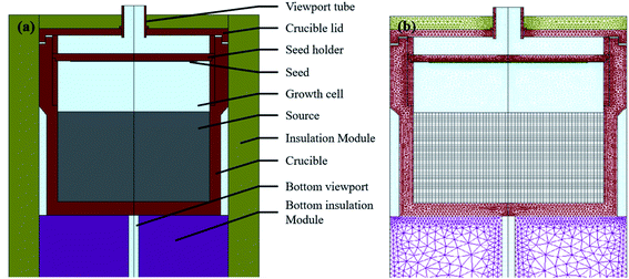 |
| | Fig. 1 (a) Structure of hot zone and (b) mesh of model. | |
Table 1 Properties of crucible materials
| Parameter |
Value |
| Bulk density/g cm−3 |
1.83 |
| Resistivity/μ Ωm |
13 |
| Dynamic modulus of elasticity/MPa |
11.5 × 10³ |
| Thermal expansion (20–200 °C)/(K−1) |
4.2 × 10⁻⁶ |
| Thermal conductivity (20 °C)/(W m−1 K−1) |
105 |
SiC crystals grow slowly under high temperature at about 2500 K with suitable temperature gradient and a low vapor pressure of 100–4000 Pa, and usually, 5–10 days are needed to obtain a 15–30 mm thick crystal. In this simulation, we used 700 μm production grade (micropipe density no more than 0.5/cm−2), 6-inch 4H type polished wafer as seed material with 4° off-orientation angle. The temperature control point was placed at the center of the seed holder's upper surface and set to 2523.15 K. Vapor pressure in the growth cell was set to 2000 Pa with 90% argon and 10% nitrogen. Frequency of induction heating was set to 10 kHz, and heating power was calculated according to the temperature and thermal properties of the entire structure. To get crystal profiles at different growth stages, we created a step every 10 hours, and the overall growth time was set to 100 hours in the initial model.
Basic mathematical models of the heat transfer process, mass transfer processes and evolution of a gas–solid crystal interface in Virtual Reactor have been described in published papers.15,16 2D axisymmetric geometry was built, and all blocks were assigned to specific materials according to real thermal field by the VR software shown in Fig. 1a. Computational grids were constructed as shown in Fig. 1b, and a total of 30![[thin space (1/6-em)]](https://www.rsc.org/images/entities/char_2009.gif) 232 mesh cells were generated. We used different density grids with different types of mesh elements (triangular and quadrilateral) for different regions to balance calculation speed and accuracy. The Navier–Stokes model was used to calculate flow dynamics, and Gebhart factors were considered to solve radiative exchange problems. In this calculation, ambient temperature was set to a constant 300 K, and we assume that the surface participates solely in radiative heat exchange. For heat transfer, residuals for RF heating and temperature are set to 1 × 10⁻⁷ and 1 × 10⁻⁶, respectively, to obtain stable convergence results.
232 mesh cells were generated. We used different density grids with different types of mesh elements (triangular and quadrilateral) for different regions to balance calculation speed and accuracy. The Navier–Stokes model was used to calculate flow dynamics, and Gebhart factors were considered to solve radiative exchange problems. In this calculation, ambient temperature was set to a constant 300 K, and we assume that the surface participates solely in radiative heat exchange. For heat transfer, residuals for RF heating and temperature are set to 1 × 10⁻⁷ and 1 × 10⁻⁶, respectively, to obtain stable convergence results.
There are more than 200 kinds of homogeneous isomers of SiC single crystal with little difference in physical properties, which makes it difficult to prepare single-structure crystals.17 4H–SiC and 6H–SiC crystals are two different polytypes that can grow stably at present, and Table 2 shows their physical properties at 300 K. 4H–SiC has a wider band gap and better thermal conductivity than 6H–SiC, showing its advantages in manufacturing power devices.
Table 2 Properties of main polytypes18,19
| Parameter |
4H–SiC |
6H–SiC |
| Crystal structure |
Wurtzite type structure |
Cubic β-ZnS structure |
| Lattice parameters/Å |
a |
3.073 |
3.073 |
| b |
10.053 |
15.118 |
| Band gap/eV |
3.230 |
3.000 |
| Melting point/°C |
2830 |
2830 |
| Thermal conductivity/(W m−1 K−1) |
480 |
360 |
| Electron mobility/(cm2 V−1 s−1) |
900 |
400 |
| Hole mobility/(cm2 V−1 s−1) |
120 |
90 |
| Breakdown field strength V cm−1 |
2 × 10⁶ |
2.1 × 10⁶ |
| Infrared refractive index |
2.55 (⊥c) |
2.55 (⊥c) |
| 2.59 (∥c) |
2.59 (∥c) |
3. Results and discussion
3.1 Physics field distribution in the crucible
3.1.1 Morphology of SiC crystal. During SiC crystal growth, flat surface shape with a little convex is crucial to avoid polytype formation and decrease internal stress, which is fatal for crystal quality. After iterative computations, profiles of SiC crystal under different growth times were obtained, as shown in Fig. 2 together with the actual crystal for comparison. The crystal growth interface shows an obvious “M” shape with polycrystal surrounding the monocrystal part (Fig. 2a). As the SiC crystal grows thicker, the “M” shape becomes more obvious, and the polycrystal (area D) grows even faster, which compresses the space of the monocrystal. The diameter of the center monocrystal portion is less than 130 mm (around area C) after 100 hours, and its maximum thickness (area A) is 20 mm with 200 μm h−1 growth rate, while the thinnest part (area B), with 9 mm thickness, is 110 mm in diameter. Unfortunately, greater convexity always implies greater internal stress.20 Meanwhile, we obtained 150 mm crystal in the lab with a convex and smooth surface within 130 mm in diameter, but polycrystal in the surrounding 130–140 mm area after the rounding treatment (Fig. 2b), which shows the consistency between experiment and simulation in shapes and profiles. This result suggests disadvantages of this hot zone in both interface shape and polycrystal propagation.
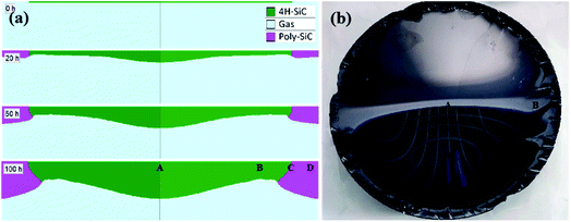 |
| | Fig. 2 (a) Crystal shape predicted at different growth times, (b) actual crystal. | |
Growth rates in different stages also illustrate this conclusion, as shown in Fig. 3. The difference along the seed is large since the initial stage. The parameter is about 320 μm h−1 at the beginning in area A and decreases rapidly to below 130 μm h−1 in the range greater than 70 diameters, while it shows an abnormal behavior in area C between 130 mm to 150 mm diameters. As the crystal grows, growth rate in the center of the seed decreases to 190 μm h−1, 160 μm h−1 and 100 μm h−1 after 20 h, 50 h and 100 h. Meanwhile, the growth rate along the radial direction becomes relatively smooth, with fluctuations evident especially in the crystal edge, which suggests that the growth conditions are not unstable, and will be discussed later.
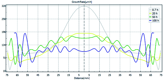 |
| | Fig. 3 Crystal growth rates in different positions at different growth times. | |
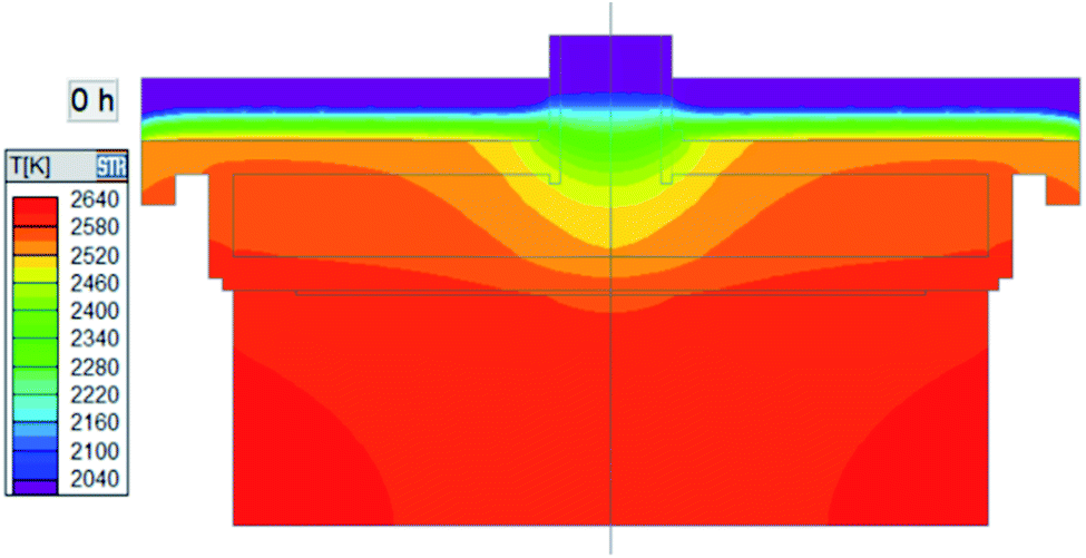
3.1.2 Temperature distribution in growth cell. Temperature has a direct influence on crystal growth, since temperature is the driving force for gas phase species transfer and deposition on crystal seed. For a general view, the initial temperature distribution of the hot zone's top part was obtained and is shown in Fig. 4. In the growth cell, the lowest value appears in center of the seed under the seed holder due to the existence of the viewport, which provides supercooling and shows a great influence on the crystal growth area in the growth cell.
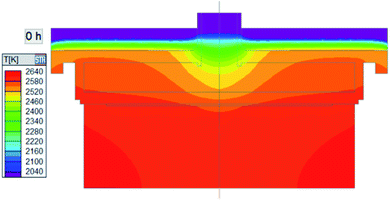 |
| | Fig. 4 Temperature distribution in the top of the crucible at initial stage. | |
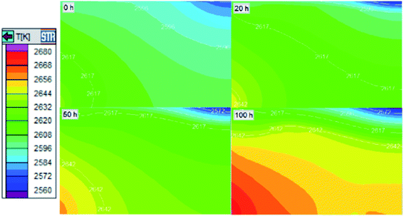
The growth cell is the chamber where gas species flow and deposition happens. The temperature distribution here at different growth stages was also obtained, as shown in Fig. 5. The highest temperature appears in SiC powder near the crucible wall, and the lowest temperature appears in the center of the SiC seed, ranging from 2560 K to 2680 K. Following the white isotherms at different times, we can find that the high-temperature zone becomes closer to the crystal as the crystal grows, which is easy to understand, as both crystal and source play important roles. When the crystal gets thicker, the thermal resistance of powder source in different parts changes simultaneously. The center of the source surface starts recrystallization, and the part close to the crucible wall undergoes graphitization. Meanwhile, the process is affected by a certain crystal thickness because the growing crystal changes heat transfer, resulting in slight “M”-shaped isotherms, just like the crystal. In other words, the temperature becomes higher, then lower, and higher again from the center to the side in a horizontal direction, which increases temperature gradients in area A and decreases temperature gradients in area B.
 |
| | Fig. 5 Temperature distribution in the growth cell at different growth times. | |
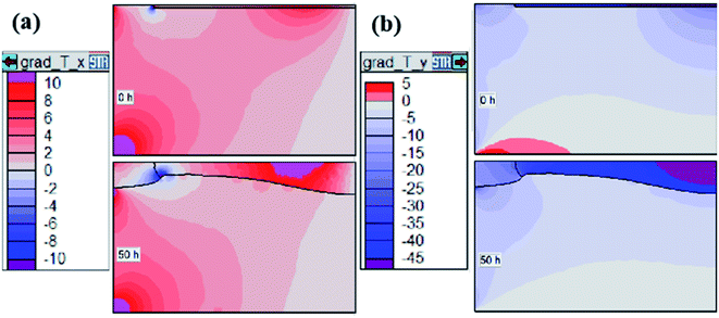
To obtain the details of temperature distribution, Fig. 6 was generated by postprocessing to show temperature gradients along the axial and radial directions. Red and blue, respectively, suggest positive and negative parameters. From powder to crystal surface, the temperature gradient along the axial direction is about 0 K cm−1 to −15 K cm−1 around the crystal, and −30 K cm−1 to −45 K cm−1 inside the crystal (Fig. 6b). The top part without SiC seed (area D in Fig. 2) has a similar temperature gradient of about −25 K cm−1, which provided a greater driving force for crystal growth with seed or polycrystal without seed. Temperature gradients along the radial direction can also explain the poor crystal interface shape (Fig. 6a). The gradient increased to above 4 K cm−1 from the center part to the side of the seed, creating a 100 mm to 120 mm diameter seed (area B) with the highest temperature and lowest temperature gradients along the axial direction. As the crystal grows, the side of the seed or the junction point of crystal, polycrystal and gas phase (area C) change violently in temperature distribution, which exacerbates the crystal edge growth state and causes small-diameter crystals with small effective thickness.
 |
| | Fig. 6 Temperature gradient distribution in the growth cell at different growth times: (a) along radial direction, (b) along axial direction. | |
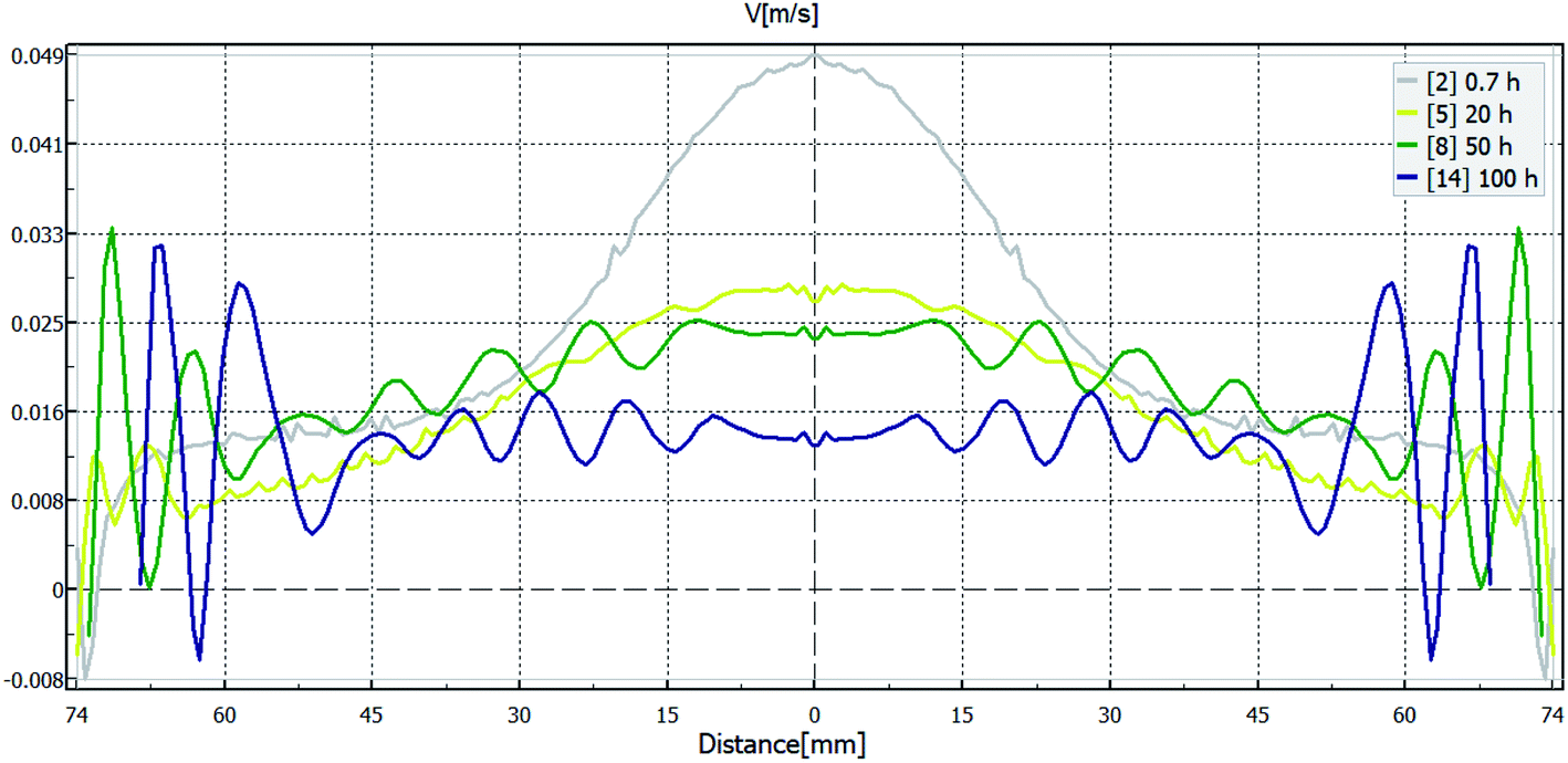
3.1.3 Flow field and velocity distribution. Guo21 put forward the field-coordination theory and pointed out that reducing the angle between velocity vector and temperature gradient is beneficial to enhance convective heat transfer and also mass transfer. Fig. 7a shows gas phase flow velocity distribution in the growth cell, with arrows in different lengths indicating the value, and Fig. 7c and d show velocity in axial direction. Since the crucible functions as the heater and the powder source locates in the high-temperature zone, gas phases such as Si, Si2C and SiC2 formed mostly in the powder side and flow to seed with low temperature. As a result, red color appears around the junction point (area C), and dark blue near the crucible wall close to the powder source surface. Meanwhile, velocity streamlines around the center of seed are perpendicular to the growth surface (Fig. 7b). What is similar to Fig. 6 is that the areas around the junction point (area C) and center of crystal (area A) have greater parameters before 50 hours, and the former velocity even reaches above 0.03 m s−1. In contrast, velocity is no more than 0.02 m s−1 in other areas of seed surface. This suggests that the temperature gradient along axial direction deeply impacts species transfer, and the crystal growth here is suppressed due to the lack of coordination between velocity and heat flow field.
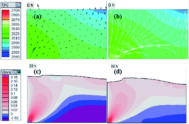 |
| | Fig. 7 (a) Temperature distribution with velocity vectors, (b) temperature distribution with velocity streamlines, (c) gas velocity distribution at 20 h, (d) gas velocity distribution at 50 h. | |
Gas flow velocity in the axial direction along the crystal diameter is shown as Fig. 8. Similar to the growth rate distribution in Fig. 3, the curve shows an inverted V-shape in beginning, and maximal value reaches 0.05 m s−1 in the center of seed. As the crystal grows thicker, velocity in the center decreases quickly and maintains at about 0.025 m s−1 due to recrystallization in the center of the SiC source surface. The law of values change matches well with growth rate in different stages, which again proves the field-coordination theory and provides an effective way to optimize crystal growth condition considering both temperature field and flow field. To understand why the velocity curve looks uneven while the crystal growth interface is relatively smooth, we compared the changes of temperature gradient and flow velocity in the early stage. At 0 h, seed temperature distribution is strongly influenced by the whole environment (Fig. 4), but the junction of seed and polycrystalline growth surface (area C) have a special condition. Seed edge grows slowly and even decomposes, while outside the edge there is a very large temperature gradient beyond −25 K cm−1, which results in the formation of an inverted V-shape outline, with the bottom of the “V” on the seed side. For the plane where the seed crystal is located, the outline becomes M-shaped, like wave lines. Because the temperature and flow velocity are affected directly by crystal shape, isotherms and contours are like two non-coincident wavy lines (Fig. 5 and 6), resulting in evident velocity fluctuation (from the junction to inside). Even if the figure shows a transient growth rate and changes gradually, we still can find residual traces (Fig. 2a).
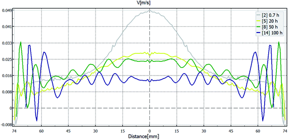 |
| | Fig. 8 Gas flow velocity around the seed in axial direction. | |
3.2 Comparison of different optimization methods
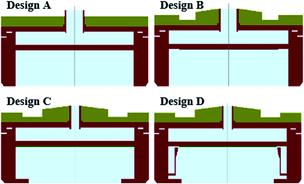
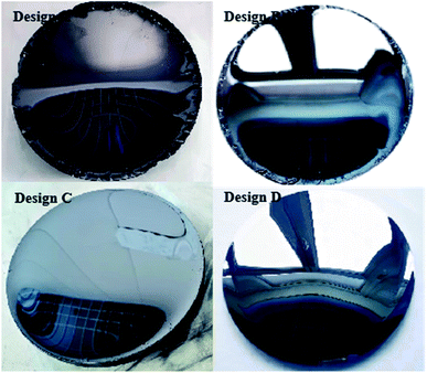
3.2.1 Temperature distribution. Focusing on temperature distribution in the growth cell and flow field distribution around the crystal, three different designs are put forward to handle the “M” surface and side polycrystal, as shown in Fig. 9. Compared with the basic design (design A), design B has different top insulation to enhance thermal insulation performance around the viewport, and designs C and D are based on design B, but have a wider groove on top, small-diameter viewport and graphite ring on the powder surface, while design C uses full-size 180 mm diameter seed, and design D uses a shelter structure where the polycrystal forms. All growth conditions are the same for these designs during the simulation and experiment, except the height of coils in design C, which is raised by 40 mm.
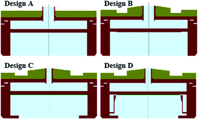 |
| | Fig. 9 Structures of different designs. | |
Temperature distributions during crystal growth were obtained and are shown in Fig. 10a. Both designs A and B have greater temperature difference, with twisting isotherms along the seed especially in the center and edge of seed, and slight blue can be found outside the edge of the seed. Compared with the former, design B shows smaller temperature change along the seed, but the isotherm still has a conspicuous “M” shape. In contrast, design C and design D have smoother isotherms especially around the crystal, which present flat, with slightly convex shape. Meanwhile, it should be pointed out that designs C and D have lower temperature, about 40 K, than design A because that small viewport makes heating power smaller in the condition where we fixed the temperature parameter in the monitor point. Besides the heating condition change, graphite ring and shelter structure play an important role in helping transfer heat to the center and influence temperature distribution both in the center and side of seed.
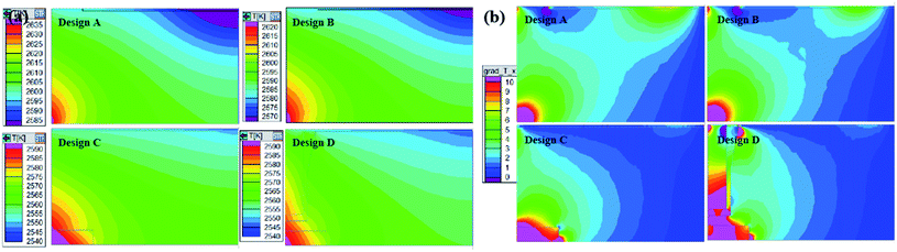 |
| | Fig. 10 (a) Temperature distribution, (b) temperature gradient distribution of different designs. | |
Fig. 10b provides a clear view of the temperature gradient along the radial direction. Blue color in the crystal means temperature along the radial direction changes a little, while red color suggests a violent increase. Unlike design A and B with about 6 K cm−1 around the seed, parameters in design C and design D in the whole crystal remain at about 1 K cm−1, which will reduce inconsistency in different areas of crystal. Around the seed edge (area C), designs A and B have negative values leading to the lowest temperature, and design D has a positive value close to the structure, which means the temperature gradient in axial direction here is negative and harmful to crystal growth. Meanwhile, greater value changes around the graphite structure show great potential to influence crystal growth conditions by changing the structure inside the crucible.
3.2.2 Flow field distribution and crystal shape. To study the angle between velocity vector and temperature gradient, the temperature and velocity streamline in the growth cell were obtained and are shown in Fig. 11. Values of velocity are presented by different colors. In area A, designs C and D have similar velocity vectors, nearly perpendicular to the temperature gradient. In areas B and C, velocity streamlines in designs C and D appear in a more vertical direction, which would carry more species to the growth interface and enhance crystal growth here. Different from designs A and B, the polycrystal in area D will no longer grow in designs C and D, because the former ones use full-size seed and the latter cannot even supply the gas species needed, limited by the shelter structure. It should be pointed out that due to lack of shelter structure guiding gas transfer, the flow velocity in design C around the seed edge has a smaller angle than in design D.
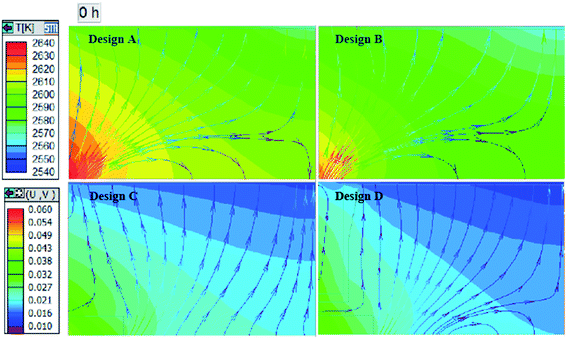 |
| | Fig. 11 Distribution of flow field of different designs. | |
Subsequent simulation calculation predicts different thickness of crystals with different deposition uniformities under the same process conditions. The profiles of crystals and crystal thickness along the radius were obtained and are shown in Fig. 12. Compared with design A, design B has a slower growth rate, about 160 μm h−1 in the center of crystal, and the difference between the thickest part and thinnest part is 6.5 mm, while it is about 11 mm in the former one. It goes without saying that we get a more uniform growth condition along the seed by changing the top insulation. As result, the polycrystal in design B is also thinner. Designs C and D show real nearly flat interface; their convexity is much smaller than both designs A and B after two process times. As expected, design C prepared a 180 mm diameter crystal with little “M” shape; there are some polytype cracks and even polycrystals produced around the seed edge near the crucible wall. Design D has 14.8 mm in the center and 9 mm in the thinnest part, showing the best profile of the four designs, benefitting from the best conditions.
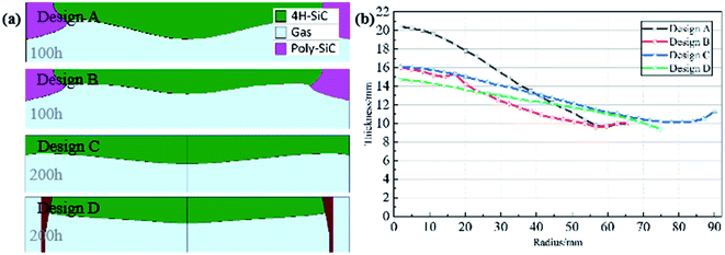 |
| | Fig. 12 (a) Profiles of SiC crystals, (b) thickness of SiC crystals. | |
3.3 Experimental crystals and test results
Under different hot-zone conditions, four crystals were prepared as shown in Fig. 13. In designs C and D, a lower gas pressure of 500 Pa was used to increase the growth rate, and the growth time was set to 150 hours. A 170 mm diameter seed obtained by expanding diameter method was used in design C, and the crucible wall thickness was slightly adjusted to adapt to the size of the seed. It is a pity that we got a crystal with edge cracks using design C, which is 15 mm in length, and the effective diameter of the crystal is about 160 mm. However, this crystal with smooth surface still shows the advantages of optimized thermal field. Design D has the best crystal shape and appearance with 16 mm effective thickness and 21 mm maximum thickness, and its growth rate increases to about 100–140 μm h−1, almost twice as much as predicted by simulation due to different vapor pressures. Anyway, these results show good consistency in crystal surface convexity and edge morphology since we focus more on trends than thickness.
 |
| | Fig. 13 Crystals of different designs. | |
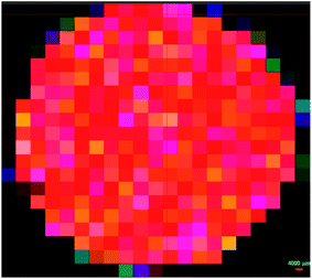
Considering that crystals A to C have polycrystals near the edge, increasing the crack risk in the process is a major concern. After multiple procedures, substrates from crystal D were obtained after chemical mechanical polishing (CMP), and the middle ones were further tested. Different SiC polytypes have different structures, so the phonon Raman spectra show obvious differences between the two polytypes. Raman spectrum scanning was used, and the mapping shows that the 4H polytype proportion of this substrate is 100% (Fig. 14), suggesting an optimized design with better field coordination plays an important role in providing stable crystal growth conditions.
 |
| | Fig. 14 Raman mapping of substrate. | |
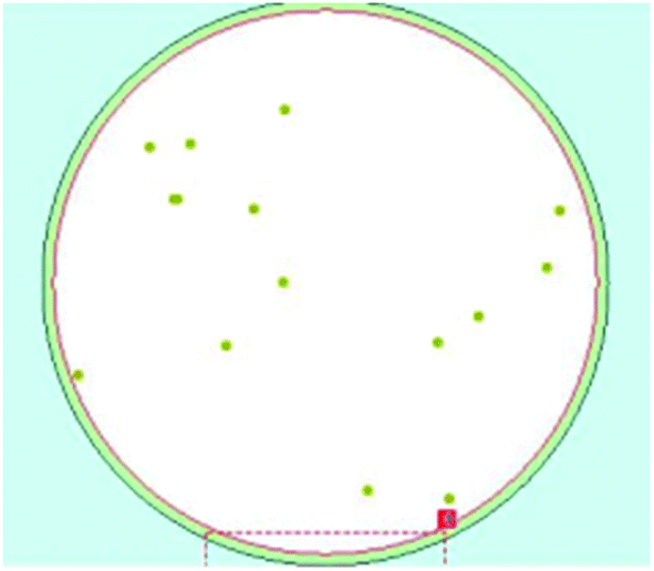
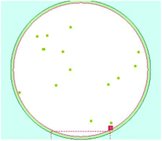
Micropipes are the main factor leading to the performance failure of SiC power devices. We used SICA88 to measure the distribution of micropipes as shown in Fig. 15, which is a common method used without any damage to the wafer. Results show a low micropipe density of about 0.09/cm−2 in this substrate, which is far better than the production grade of the industry standard. These results indicate that maintaining stable step flow growth is conducive to healing micropipe defects. Since the formation of micropipes is related to the growth conditions and seed crystal, the research proved the feasibility of zero micropipe crystal preparation using low-grade seed, which requires more work to do.
 |
| | Fig. 15 Micropipe distribution of substrate. | |
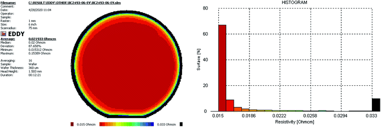
Conductivity is a key indicator of conductive crystals. We use a noncontact and nondestructive eddy current method to test its resistivity, as shown in Fig. 16. Results show that the average resistivity is 0.022 Ohm cm, meeting the industry requirements of 0.015–0.025 Ohm cm. 80% of surfaces have resistivity no more than 0.017 Ohm cm, and large values appear only at the edge of the wafer, about several millimeters, showing great distribution uniformity.
 |
| | Fig. 16 Resistivity distribution of substrate. | |
Geometric parameters of the wafer reflect both the post-processing technology and internal stresses of the crystal. Surface geometric parameters were measured using the Tropel FlatMaster, as shown in Fig. 17. The wafer has small values for the bow and warp parameters, 1.8 μm and 10.9 μm, respectively. Meanwhile, it has good surface flatness too, with a total thickness deviation of 2.6 μm and maximum local thickness deviation of 1.5 μm. This result clearly suggests a high quality of this crystal with a nearly flat and slightly convex interface.
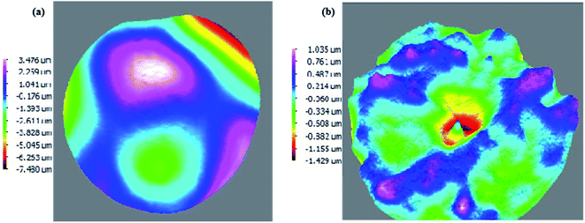 |
| | Fig. 17 Surface characterization of substrate: (a) bow/warp @3700×, (b) flatness @17000×. | |
4. Conclusion
We have established a model of the growth process of large-size silicon carbide crystals using a numerical approach. The crystal morphology predicted by the simulation matches well with the experimental crystals. After studying the changes in the growth interface and the distribution of physical fields during the growth process, distributions of thermal field and flow field are optimized to meet field-coordination effects, and a nearly flat and slightly convex growth interface was obtained. A high-quality 150 mm single crystal with a center thickness of 21 mm was prepared using the optimized thermal field, with micropipes less than 0.1 cm−2 and a uniform resistivity distribution. Our work introduces the variation characteristics of temperature fields and so on during the growth of silicon carbide crystals, and provides a simple and feasible method to improve the quality of large-sized single crystals using the PVT method.
Conflicts of interest
The authors declare that they have no known competing financial interests or personal relationships that could have influenced the work reported in this paper.
Acknowledgements
This work was supported by National Key Research and Development Program of China (No. 2021YFB3401602), Major Scientific and Technological Achievements Transformation Projects of Heilongjiang Province of China (No. CG20A008) and Natural Science Foundation of Heilongjiang Province (Grant No. JQ2019E003). We thank Soft-Impact China (Harbin), Ltd, for its support in simulation content.
References
- R. Kirschman, Status of Silicon Carbide (SiC) as a WideBandgap Semiconductor for High Temperature Applications: A Review, Wiley-IEEE Press, 2009 Search PubMed.
- J. B. Casady and R. W. Johnson, Status of Silicon Carbide (SiC) as a Wide-Bandgap Semiconductor for High-Temperature Applications: A Review, Solid-State Electron., 1996, 39(10), 1409–1422 CrossRef.
- T. Kato, T. Miura and I. Nagai, et al. Enlargement Growth of Large 4H-SiC Bulk Single Crystal, Mater. Sci. Forum, 2011, 679–680, 3–7 CAS.
- J. Quast, D. Hansen and M. Loboda, et al. High Quality 150 Mm 4H SiC Wafers for Power Device Production, Mater. Sci. Forum, 2015, 821–823, 56–59 Search PubMed.
- P. T. B. Shaffer, A Review of the Structure of Silicon Carbide, Acta Crystallogr., 2010, B25(3), 477–488 Search PubMed.
- M. Nakabayashi, T. Fujimoto and M. Katsuno, et al. Growth of Crack-Free 100mm-Diameter 4H-SiC Crystals with Low Micropipe Densities, Mater. Sci. Forum, 2008, 600–603, 3–6 Search PubMed.
- Z. G. Herro, B. M. Epelbaum and M. Bickermann, et al. Effective Increase of Single-Crystalline Yield During PVT Growth of SiC by Tailoring of Temperature Gradient, J. Cryst. Growth, 2004, 262(1–4), 105–112 CrossRef CAS.
- A. Arora, A. Pandey and A. Patel, et al. Polytype Switching Identification in 4H-SiC Single Crystal Grown by PVT, J. Mater. Sci.: Mater. Electron., 2020, 31(19), 16343–16351 CrossRef CAS.
- Y. Goldberg, M. E. Levinshtein and S. L. Rumyantsev, Properties of Advanced Semiconductor Materials: GaN, AIN, InN, BN, SiC, SiGe, John Wiley, 2001 Search PubMed.
- R. H. Ma, Q. S. Chen and H. Zhang, et al. Modeling of Silicon Carbide Crystal Growth by Physical Vapor Transport Method, J. Cryst. Growth, 2000, 211(1/4), 352–359 CrossRef CAS.
- T. Wejrzanowski, J. Dagiel and M. Grybczuk, Modeling of Growth Kinetics of SiC Single Crystal in PVT Process, 17th International Conference on Crystal Growth and Epitaxy, 2013 Search PubMed.
- R.-H. Ma, H. Zhang, S. Ha and M. Skowronski, et al., Integrated Process Modeling and Experimental Validation of Silicon Carbide Sublimation Growth, J. Cryst. Growth, 2003, 252(4), 523–537 CrossRef CAS.
- Y. Tawada, K. Tsuge and M. Kondo, Properties and Structure of a-SiC:H for High-Efficiency a-Si Solar Cell, J. Appl. Phys., 1982, 53(7), 5273–5281 CrossRef CAS.
- A. A. Lebedev, Deep Level Centers in Silicon Carbide: A Review, Semiconductors, 1999, 33(2), 107–130 CrossRef CAS.
- M. V. Bogdanov, A. Galyukov and S. Y. Karpov, Virtual Reactor: A New Tool for SiC Bulk Crystal Growth Study and Optimization, Materials Science Forum, 2001 Search PubMed.
- C. Yang, G. Liu, C. Chen, Y. Hou, M. Xu and Y. Zhang, Numerical Simulation of Temperature Fields in a Three-Dimensional SiC Crystal Growth Furnace with Axisymmetric and Spiral Coils, Appl. Sci., 2018, 8(5), 705 CrossRef.
- P. Gao, J. Xin and X. Liu, et al. Control of 4H Polytype of SiC Crystals by Moving Up the Crucible to Adjust the Temperature Field of the Growth Interface, CrystEngComm, 2019, 21(12), 6964–6968 RSC.
- G. Dhanaraj, X. R. Huang, M. Dudley, et al., Silicon Carbide Crystals——Part I: Growth and Characterization–ScienceDirect, Crystal Growth Technology, 2003, 181–232 Search PubMed.
- I. A. Zhmakin, A. V. Kulik and S. Y. Karpov, et al. Evolution of Thermoelastic Strain and Dislocation Density During Sublimation Growth of Silicon Carbide, Diamond Relat. Mater., 2000, 9(3–6), 446–451 CrossRef CAS.
- J. W. Choi, J. G. Kim, B. K. Jang, et al., Modified Hot-Zone Design for Large Diameter 4H-SiC Single Crystal Growth: European Conference on Silicon Carbide and Related Materials, 2019 Search PubMed.
- G. Zengyuan, Mechanism and Control of Convective Heat Transfer, Chinese Science Bulletin, 2001 Search PubMed.
|
| This journal is © The Royal Society of Chemistry 2022 |
Click here to see how this site uses Cookies. View our privacy policy here. 
 Open Access Article
 This Open Access Article is licensed under a Creative Commons Attribution-Non Commercial 3.0 Unported Licence
 a,
Guofeng Fanb,
Tie Lic and
Lili Zhao*a
a,
Guofeng Fanb,
Tie Lic and
Lili Zhao*a