DOI:
10.1039/D2RA02868A
(Paper)
RSC Adv., 2022,
12, 19695-19702
Polyimide-derived graphite barrier layer adhered to seed crystals to improve the quality of grown silicon carbide†
Received
6th May 2022
, Accepted 26th June 2022
First published on 6th July 2022
Abstract
A facial method was developed to in situ fabricate a graphite layer on a SiC seed crystal to reduce the formation of defects during the growth of SiC ingots. The formulated PI matrix combined with an appropriate coupling agent could strongly adhere to SiC and be transformed into protective layers for SiC seed crystals during SiC growth. The thermally conductive graphite layers on SiC effectively reduce the backside diffusion of Si, inhibit the loss of Si from seed crystals during high-temperature growing process, and consequently lead to fewer defects formed in the SiC ingot. The graphitization degree, chemical state, roughness and morphology of films were investigated in this work.
Introduction
A wide band gap semiconductor, such as silicon carbide (SiC), has been considered a potential candidate material for modern electronic devices, where high efficiency and low loss for high-frequency and high-speed power conversion are required.1,2 In addition, the demand for SiC has increased in high-speed computing and high-power applications due to its higher thermal conductivity and higher breakdown electric field strength than traditional Si-based materials.3,4
The fabrication of high quality SiC is difficult and the physical vapor transport (PVT) growth is the most successful method to obtain large-scale SiC crystals.3–5 As illustrated in Scheme 1, SiC source powders sublime at an extremely high temperature from the bottom of a graphite crucible and the vapor species gradually deposit on a SiC seed holding at the top of the graphite crucible.3 Unfortunately, cavities are commonly formed in seed crystals during SiC growth process due to the thermal decomposition and the backside diffusion of Si-contained species from the seed under temperature gradients. The cavities of the seed then lead to the formation of defects in the grown SiC ingots.6,7 To prevent the existence of gaps or voids between the seed crystal and the seed holder in the graphite crucible, the backside of the SiC seed crystal could be covered with a thin carbon-based layer, organic glues, or resin mixing with graphite powders before attaching to the seed holder.5,8–10
As the presence of a diffusion barrier on the backside of the seed crystal is a promising approach to the formation of high-quality SiC ingot, we tried to develop a thermally conductive barrier layer on the backside of SiC seed substrate to maintain the condition of seed crystal and consequently improve the quality of grown SiC ingots.
Aromatic PI has been a potential precursor for the fabrication of graphite films due to its low coefficient of thermal expansion, high carbon yield and easy graphitization.11–13 It has been reported that the dimension of PI-derived graphite film remains and the formation of hexagonal honeycomb lattice of layer-by-layer graphite structure without cracking can be achieved via catalyst- or filler-added carbonization and graphitization.12–22
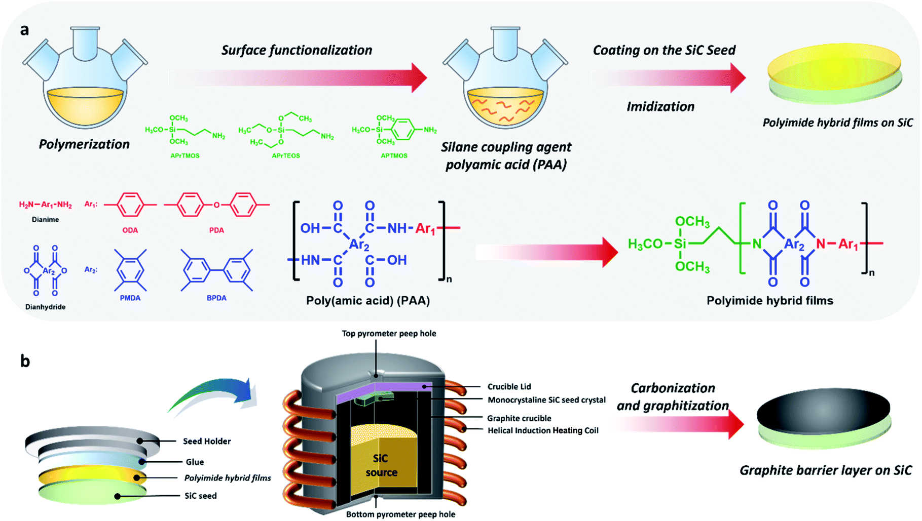
In this work, we formulated the precursor of PI and then directly coated on a SiC substrate, which is the SiC seed crystal for the growing of SiC. Four types of PI films with different dianhydrides and diamines were synthesized, and their properties were compared. To increase the adhesion strength between PI film and SiC seed substrate, three kinds of silane coupling agents were introduced to the PI matrix and resultant performance were compared. Without the addition of other promotors, a designated carbonization and graphitization process was applied to the coated PI-silane hybrid film on SiC attaching to a graphite seed holder. The characteristics of resultant graphite films on SiC substrate and the formulation of PI precursor were investigated. The improved barrier property of PI-derived graphite films reduced the formation of defects in SiC seed during the growth of SiC ingots and thus the quality of SiC ingots could be enhanced. The coating and graphitizing PI precursor on SiC also demonstrated its potential for scale production of high-quality SiC crystals.
Experimental
Materials
Two dianhydride monomers, pyromellitic dianhydride (PMDA, 97%) and 3,3′-biphenyltetracarboxylic dianhydride (BPDA, 97%) were purchased from SIGMA-ALDRICH. They were recrystallized by acetic anhydride and vacuum dried at 120 °C for 24 h before usage. The two diamine monomers, 4,4′-oxydianiline (ODA, 97%) and p-phenylenediamine (PDA, 99%) from SIGMA-ALDRICH were used as-received. The solvent, 1-methyl-2-pyrrolidone (NMP, 99.5%) was purchased from TEDIA. The coupling agents, 3-aminopropyl-trimethoxysilane (APrTMOS, 97%) and 3-aminopropyl- triethoxysilane (APrTEOS, 99%), were purchased from SIGMA-ALDRICH, and p-aminophenyl-trimethoxysilane (APTMOS, 90%) was obtained from GELEST. The silicon carbide (SiC) wafer was provided from National Chung-Shan Institute of Science & Technology (NCSIST).
Fabrication of PI-silane hybrid films on SiC wafer
The polyamic acid (PAA) solution was first synthesized by dissolving 1.11 mol of diamine (ODA or PDA) in suitable amounts of NMP and then gradually mixing with 1 mol of dianhydride (PMDA or BPDA). After continuously stirring at room temperature for 2 h under nitrogen, the PAA solution was ready for the addition of a coupling agent. The following sample films derived from the PAA solution containing PMDA and ODA were denoted PM-O. Similarly, the BP-P indicated the components of BPDA and PDA in PI matrix.
Fixed amounts (0.2275 mol) of silane coupling agents (APrTMOS, APrTEOS, or APTMOS) were diluted by NMP and then mixed with the above PAA solution at room temperature under nitrogen for 2 h to obtain the PAA-silane solution with a solid content of 15 wt% for the following spin-coating on SiC. The two-step spin coating process, 1000 rpm (10 s) and 4000 rpm (10 s), was applied to homogeneously coat pure PAA or PAA-silane wet films on SiC. The following curing process was performed in an air-circulating oven maintaining at each temperature (80 °C, 100 °C, 210 °C, 250 °C, and 300 °C) for 1 h to complete the imidization process of pure PI or PI-silane hybrid films. The PI-silane hybrid films were denoted by adding the notation of SiCH3, SiC2H5, or SiPh (for APrTMOS, APrTEOS, or APTMOS) after the abbreviated monomers. For example, the PI-silane hybrid film named PM-O–SiCH3 indicated the selection of dianhydride PMDA, diamine ODA, and coupling agent APrTMOS.
Carbonization and graphitization process of PI-silane films on SiC
The surface of the SiC-supported PI-silane hybrid film was fully covered with an artificial graphite plate and then placed in a quartz tubular furnace to carbonize hybrid films under argon. The carbonization procedure was set as follows: (1) heating from room temperature (about 28 °C) to 550 °C at a heating rate of 3 °C min; (2) heating from 550 °C to 800 °C at a heating rate of 0.5 °C min; (3) heating from 800 °C to 1000 °C at a heating rate of 1 °C min; (4) heating at 1000 °C for 1 h; (5) cooling from 1000 °C to 300 °C at a cooling rate of 10°C min; (6) natural cooling from 300 °C to room temperature. The carbonized film was named by adding the letter C to the original name of the film, e.g. PM-O–SiCH3-C, and BP-P–SiCH3-C. For the final graphitization process, the carbonized film was also covered with an artificial graphite plate and then using a graphite furnace to graphitize film. The heating procedure was as follows: (1) heating from room temperature (about 28 °C) to 1150 °C at a heating rate of 5 °C min−1 under the vacuum of 8 × 10⁻⁵ torr; (2) heating at 1150 °C for 30 min under the vacuum of 8 × 10⁻⁵ torr; (3) purging argon and controlling the pressure at 600 torr at 1150 °C ; (4) heating from 1150 °C to 2200 °C at a heating rate of 3°C min−1 under the vacuum of 10 torr; (5) heating at 2200 °C for 2 h under the 10 torr; (6) natural cooling from 2200 °C to room temperature. The graphitized film was named by adding the letter G to the original name of the film, e.g. PM-O–SiCH3-G, and BP-P–SiCH3-G.
Characterization
The morphology of the surface and cross-section of the films were observed by a scanning electron microscope (SEM, JEOL, JSM-7100F) and a white light interference (WLI) microscope (ZYGO, NEWVIEW 8300). The average roughness (Sa) and root mean square roughness (Sq) of each coating on SiC were measured from its WLI image. The Fourier transform infrared (FTIR) spectra of samples were recorded by an infrared spectrophotometer (JASCO, FTIR-4600) using the resolution of 4 cm−1 and the scan number of 64 scans. An X-ray photoelectron spectrometer (XPS, ULVAC, PHI 5000) was utilized to identify the chemical structures on films. The thermal mechanical analyzer (TMA, TA Instruments, Q400) was performed at a tensile force of 0.1 N and a heating rate of 10 °C min−1 from 30 to 400 °C to obtain the coefficient of thermal expansion (CTE) of each film in the temperature range of 55 to 250 °C. The thermogravimetric analyzer (TGA, TA Instruments, Q500) was conducted at a heating rate of 20 °C min−1 from 30 to 800 °C under nitrogen (or air) to determine the char yield and the thermal degradation temperature (Td) at 5% weight loss. A Raman micro spectroscopy system (Tokyo Instruments, Nanofinder 30) with a He–Ne Laser (632.8 nm) was used to investigate the degree of defects of each film under the scanning range of 1200 to 2800 cm−1. An X-ray diffractometer (Malvern Panalytical, X'Pert3 Powder) was used to examine the crystalline structure of films.
Results and discussion
Formulation of PI matrix for a proper graphite barrier layer on SiC
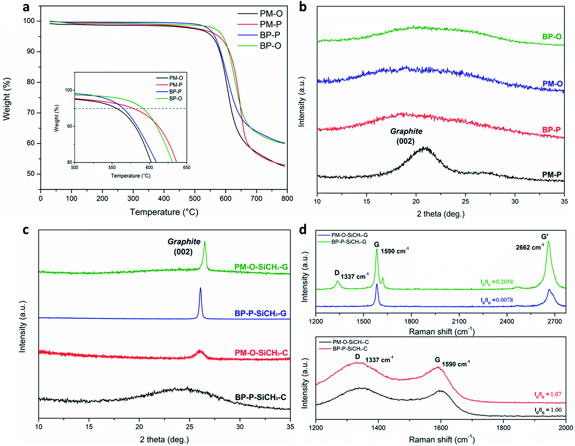
In this work, four kinds of PI films with various monomers were synthesized and then graphitized into graphite films under the same parameters. Therefore, the theoretical carbon contents and char yields of PI precursor are critical factors affecting the quality of the derived graphite films.12,14 As listed in Table 1, the theoretical carbon contents of each PI matrix were ranging from 72 to 76% and the residual weight percentage at 800 °C (RW800) from the TGA curve (Fig. 1(a)) of each film was higher than 53%. The results suggested the selected PI matrix could potentially maintain shape and structure during the conversion to graphite structure.12–14 On the other hand, the planarity of the repeating unit and film-forming property (formability) of PI films were also indicators for the quality of resultant graphite films.14 The absence of etheric oxygen within PM-P matrix made it the most rigid PI matrix and highest planar repeating units among others, however, exhibiting very poor film-forming property. Moreover, consistent results were obtained from XRD patterns shown in Fig. 1(b). The rigid benzene rings made PM-P exhibit the highest crystallinity among. Cracks appeared after imidization of PM-P matrix that it was not a qualified candidate precursor as a protection barrier layer on SiC.
Table 1 Characteristics of PI filmsa
| Sample |
Formability |
Theoretical carbon content (%) |
RW800 (%) |
CTE (ppm °C−1) |
Tg (°C) |
Roughness (μm) |
| Sa |
Sq |
| +: the film showed good film-forming property. −: the film showed poor film-forming property. n/a: didn't conduct the measurement due to poor film-forming property. |
| PM-O |
+ |
71.75 |
53.14 |
33 |
353 |
0.005 |
0.007 |
| PM-P |
− |
76.43 |
53.45 |
n/a |
n/a |
0.005 |
0.013 |
| BP-O |
+ |
76.44 |
60.18 |
55 |
263 |
0.006 |
0.037 |
| BP-P |
+ |
74.89 |
60.17 |
3 |
283 |
0.006 |
0.017 |
 |
| | Fig. 1 (a) TGA curves and (b) XRD patterns of a series of PI films derived from different monomers. (c) XRD patterns and (d) Raman spectra of carbonized or graphitized PI hybrid films. | |
The adhesion strength between PI coatings on SiC was evaluated by the cross-cut method. As shown in Fig. S1 in the ESI,† a classification of 0B was assigned to all PI coatings on SiC due to a significant removal ratio (>65%) was obtained from all coatings. As evidenced from WLI images, very low surface roughness was obtained from all PI films and consequently led to poor adhesion of PI on SiC substrates. Therefore, the silane coupling agents were introduced into the PI matrix to improve the adhesion strength. The cross-cut testing results (Fig. S2†) showed that none of the cross-cut areas was removed, which is the classification of 5B, from all PI-silane hybrid films coated on SiC. However, the addition of the soft segments of silane within a relatively rigid PI matrix led to an increase in CTE values. The TMA results (Fig. 2) indicated the estimated value of CTE of pure PI film ranking from low to high was BP-P, PM-O, and then BP-O. Although BP-O possessed higher theoretical carbon contents and char yields, the highest CTE value (55 ppm K−1) made it not a suitable matrix as a protective barrier layer on SiC. In summary, only PM-O and BP-P series were chosen for the following carbonization and graphitization processing.
 |
| | Fig. 2 TMA curves of PI films and PI-silane hybrid films. Insets: the dimension changes of films in the temperature range of 50 to 250 °C. | |
Effects of coupling reagents on the stability of carbonized coatings on SiC
For the energy-saving concern, the manufacturer initially carbonizes the barrier coatings on SiC seed substrates and then simultaneously graphitizes them into the protective layers during the growth of SiC crystals. Therefore, the stability of carbonized PI-hybrid films on SiC under storage at ambient conditions was evaluated. Fig. 3 shows the images of 3 kinds of silane-contained BP-P films after carbonization and changes between different storage periods (0 ∼ 49 days) at room temperature. The wrinkles from the edges of BP-P-SiC2H5–C and BP-P-SiPh-C appeared after 3 days. In contrast, a smooth surface throughout the film even after 49 days storage was revealed from BP-P–SiCH3-C. The results suggested that the adhesion of SiC to the film containing -SiCH3 was relatively stable.
 |
| | Fig. 3 The images of (a) BP-P–SiCH3-C, (b) BP-P-SiC2H5–C (c) BP-P-SiPh-C films on SiC at different storage time: (a–c) 0 day (as-prepared), (d–f) 7 days, and (g–i) 49 days. | |
Graphitization degree of coatings on SiC
The XRD patterns of PM-O–SiCH3 and BP-P–SiCH3 after carbonization and graphitization were shown in Fig. 1c. The diffraction peak at around 26.5° is considered as the ideal (002) graphite crystalline with the d spacing of 0.3354 nm, according to Bragg's equation.10,20,23,24 Broad peaks were observed from PM-O–SiCH3-C and BP-P–SiCH3-C films as amorphous carbon structures still existed in the carbonized films. In contrast, the diffraction peak of (002) facets turned narrow from both 2200 °C-graphitized films PM-O–SiCH3-G and BP-P–SiCH3-G. The position of the diffraction peak of (002) and the value of interlayer spacing at (002) (d002) of each film were compared and listed in Table 2. For PM-O–SiCH3-G, the graphite peak (002) was at 2θ = 26.48°, corresponding to the d-spacing of 0.3365 nm. On the other hand, the d-spacing was 0.3419 nm for BP-P–SiCH3-G. The decrease in d-spacing indicated the increase in graphitization degree.17,20,23–27 The degree of graphitization was further estimated, according to the following empirical formula.16,23,25,28
Table 2 Characteristics of PI-silane coatings on SiC after carbonization or graphitizationa
| Sample |
Formability |
R (ID/IG) |
2θ (°) |
d002 (nm) |
Degree of graphitization (%) |
Roughness (μm) |
| Sa |
Sq |
| +: the film showed good film-forming property. −: the film showed poor film-forming property. n/a: didn't conduct the measurement. The value was beyond the scope of the formula. |
| PM-O–SiCH3-C |
+ |
1.00 |
25.94 |
0.3434 |
6.9 |
0.005 |
0.007 |
| PM-O–SiCH3-G |
+ |
0.0078 |
26.48 |
0.3365 |
87.2 |
0.900 |
1.453 |
| BP-P–SiCH3-C |
+ |
1.07 |
24.78 |
0.3592 |
0b |
0.001 |
0.003 |
| BP-P–SiCH3-G |
− |
0.2058 |
26.06 |
0.3419 |
24.4 |
2.575 |
3.213 |
As summarized in Table 2, a graphitization degree of 87% was achieved from PM-O–SiCH3-G and 24% from BP-P–SiCH3-G. Notably, the graphitization degree of in situ graphitized graphite film PM-O–SiCH3-G without the addition of promotors or catalysts was relatively higher than most literature values.17,20,24 The quality of graphite structure on SiC was also examined by Raman spectra (Fig. 1d). The presence of D band indicated the existence of defects or disorder structures within films. On the other hand, G band was attributed to the stretching of all sp2 bonding atoms from hexagonal rings of graphite structure.25 The ratio in the intensity of D band to G band (R = ID/IG) was an indicator of quality of graphite matrix. As listed in Table 2, the R values for carbonized films PM-O–SiH3-C and BP-P-SiH3-C were larger than 1, and then reduced to around 0.5 after graphitization. The PM-O–SiCH3-G exhibited a lower R value (0.0078) than BP-P–SiCH3-G (0.2058), which is consistent to the above ranking of graphitization degree calculated from d-spacing. Although the sheet resistance of coatings depended on thickness, these values of PM-O–SiCH3-G and BP-P–SiCH3-G were also provided in Table 2. The coating of high-quality graphite film (PM-O–SiCH3-G) on SiC showed the potential to prevent backside diffusion of Si from SiC substrates during the high-temperature SiC-growing process.
Surface elements of PI coatings on SiC before and after graphitization
The elemental changes on SiC substrate during four stages were monitored via XPS analysis. As shown in Fig. 4, the signals of C, Si, and O elements were intense from SiC substrates and then the intensity of Si significantly decreased from 23.9 atomic% to 2.5 atomic% after the coating of PM-O–SiCH3 on SiC. After carbonization or graphitization, the reduction in the amounts of N and O was observed due to the escaping of N- and O- contained gaseous species from PI matrix. The atomic ratio of N on PM-O–SiCH3 was 5.6% and reduced to 0.8% and less than 0.1% for PM-O–SiCH3-C and PM-O–SiCH3-G, respectively. The content of O on PM-O–SiCH3-G was only 3.7 atomic%, comparing to 12.7% and 17.9% for PM-O–SiH3-C and PM-O–SiH3, respectively. The content of C on PM-O–SiCH3-G was as high as 94.3 atomic%, which is 10% larger than the value obtained from PM-O–SiCH3-C. The elemental analysis on coatings again confirmed the successful graphitization of formulated PI films and coverage on SiC.
 |
| | Fig. 4 XPS survey spectra of SiC substrate, PI hybrid film (PM-O–SiCH3), carbonized and graphitized films (PM-O–SiCH3-C and PM-O–SiCH3-G). | |
The high resolution XPS spectra in C1s, N1s and O2p regions together with the deconvolution results for the PM-O–SiCH3, PM-O–SiCH3-C and PM-O–SiCH3-G on SiC were provided in Fig. S3.† The XPS C1s spectra of PM-O–SiCH3 could be deconvoluted into three peaks, C![[double bond, length as m-dash]](https://www.rsc.org/images/entities/char_e001.gif) C, C–C, and N–CO.16,29 After graphitization, the sp2-and sp3-carbon (CC/C–C) ratio on PM-O–SiCH3-G increased, which is consistent to Raman results. Moreover, Π-Π interaction at 290.8 eV revealed and N–CO signal disappeared from PM-O–SiCH3-G. The N1s signals were barely detected from the graphitized sample PM-O–SiCH3-G because of the high degree of graphitization. In contrast, three N-containing groups were revealed from PM-O–SiCH3-C due to the residue of PI matrix after carbonization.30 The Si–O–Si and CO groups were deconvoluted from XPS O1s spectra of PM-O–SiCH3. With the following carbonization and graphitization process, significant decrease in CO and increase in Si–O–Si were observed. Similarly, the Si–O groups were revealed from Si2p spectra of PM-O–SiCH3 due to the presence of silane coupling reagents in PI matrix. Notably, the presence of Si–O–C groups on carbonized PI-hybrid films indicated the improvement in adhesion strength of coatings on SiC.31
C, C–C, and N–CO.16,29 After graphitization, the sp2-and sp3-carbon (CC/C–C) ratio on PM-O–SiCH3-G increased, which is consistent to Raman results. Moreover, Π-Π interaction at 290.8 eV revealed and N–CO signal disappeared from PM-O–SiCH3-G. The N1s signals were barely detected from the graphitized sample PM-O–SiCH3-G because of the high degree of graphitization. In contrast, three N-containing groups were revealed from PM-O–SiCH3-C due to the residue of PI matrix after carbonization.30 The Si–O–Si and CO groups were deconvoluted from XPS O1s spectra of PM-O–SiCH3. With the following carbonization and graphitization process, significant decrease in CO and increase in Si–O–Si were observed. Similarly, the Si–O groups were revealed from Si2p spectra of PM-O–SiCH3 due to the presence of silane coupling reagents in PI matrix. Notably, the presence of Si–O–C groups on carbonized PI-hybrid films indicated the improvement in adhesion strength of coatings on SiC.31
Morphology of PI coatings on SiC after carbonization and graphitization
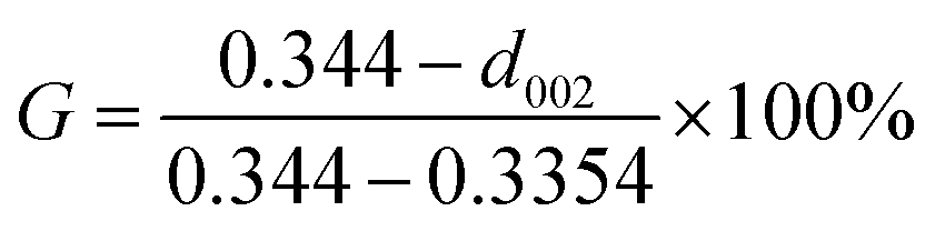
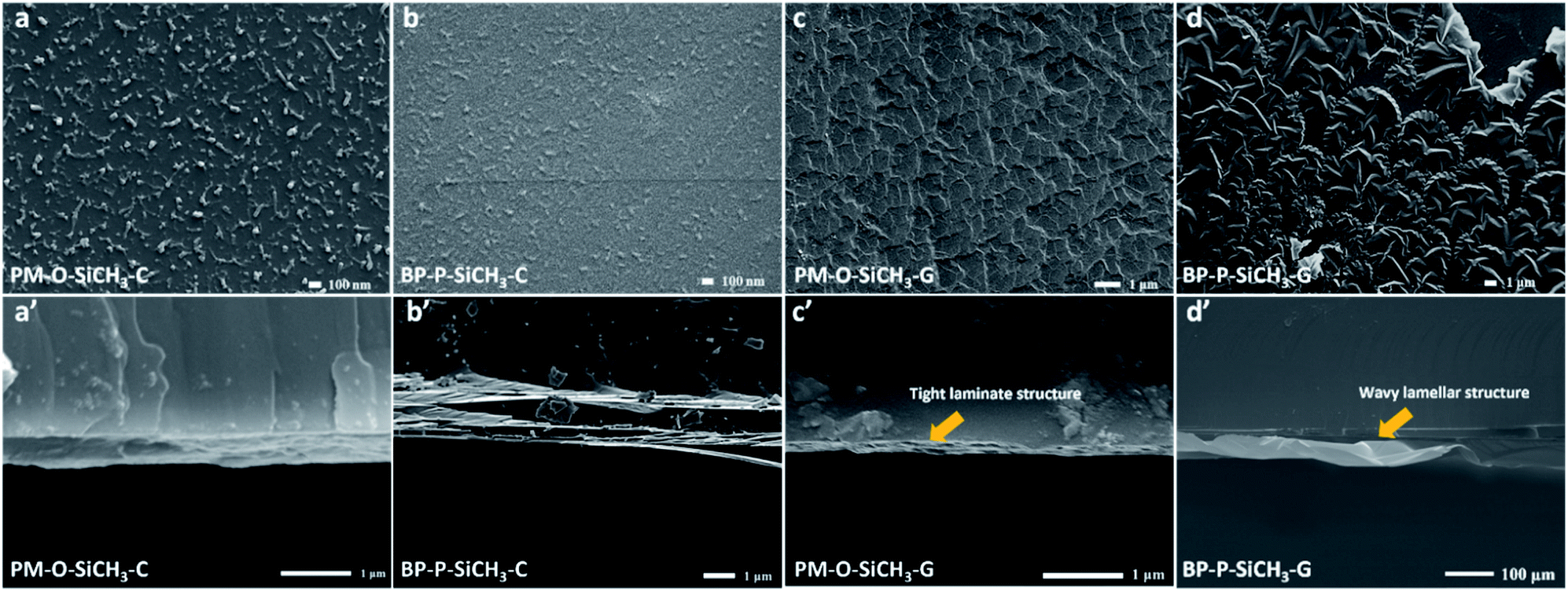
The morphology of each PI hybrid coating on SiC substrate was revealed from the SEM images shown in Fig. 5. During the carbonization process, PI matrix undergoes pyrolytic reformation to produce large numbers of gas molecules thus causing surface bulges and defects.23,32 Therefore, as shown in Fig. 5(a and b), a lot of stripes and white granular objects appeared on PM-O–SiCH3-C and BP-P–SiCH3-C. The corresponding cross-sectional images shown in Fig. 5(aʹ and bʹ) presented looser layered structure from PM-O–SiCH3-C, while more compact layers were obtained from BP-P–SiCH3-C. However, the delamination of BP-P–SiCH3-C from SiC substrate was observed Fig. 5(bʹ). During graphitization process, the amorphous carbon started to form basic structural units with 10 to 20 planar rings and then reformed into two-dimensional ordered layers.33,34 The change in the morphology after graphitization was observed from Fig. 5(c and cʹ), where the surface of PM-O–SiCH3-G was replaced by well stacked lamellar structure. On the other hand, substantial wave-like undulations and cracks appeared from BP-P–SiCH3-G (Fig. 5(d and dʹ)). The comparison of the morphology of those coatings on SiC suggested that PM-O–SiCH3-G could completely cover the surface of SiC to serve as an efficient protective layer for Si diffusion. The 3D profiles shown in Fig. 6 are the surface height for samples with a specific scanning area. The surface roughness (Sa or Sq) of each coating on SiC was calculated from the variation of surface height.35 As shown in Table 1, the difference in the surface roughness of PI coatings derived from various monomers was negligible. An average roughness of 0.0005 to 0.0006 μm was obtained from all PI coatings on SiC. After graphitization, the surface roughness of PM-O–SiCH3-G and BP-P–SiCH3-G significantly increased to 0.9 and 2.575 μm, respectively (Table 2). The increase in roughness facilitated the adhesion of graphitized film to SiC.
 |
| | Fig. 5 Top-view SEM images of coatings (a) PM-O–SiCH3-C, (b) BP-P–SiCH3-C, (c) PM-O–SiCH3-G, (d) BP-P–SiCH3-G on SiC substrates. The corresponding cross-sectional SEM images of each coating are shown in (a'), (b'), (c'), (d'). | |
 |
| | Fig. 6 WLI images of (a) PM-O–SiCH3-C, (b) BP-P–SiCH3-C, (c) PM-O–SiCH3-G, (d) BP-P–SiCH3-G, (e) PM-O, (f) PM-P, (g) BP-O, (h) BP-P films on SiC. | |
The barrier property of PM-O–SiCH3-G and BP-P–SiCH3-G on SiC
To evaluate the barrier property of PM-O–SiCH3-G and BP-P–SiCH3-G coatings on SiC, each graphite layer-coated SiC seed substrate was held at the top of the graphite crucible to complete the SiC growing process designed by NCSIST (Scheme 1). As shown in Fig. 7(a), the perfect graphite layer remained on SiC seed after SiC growing indicating successful prevention of backside diffusion of Si by the PM-O–SiCH3-G film on SiC seed substrate. In contrast, a relatively rough surface and desilication cavities were observed from the SiC seed coating with BP-P–SiCH3-G (Fig. 7(b)). After the crystal growth process, the thermal decomposition and disintegration of the SiC seed could be effectively inhibited as well as the Si diffusion rate could be reduced by coating a thermally conductive graphite layer derived from a PI coating with the formulation of PM-O–SiCH3.
 |
| | Scheme 1 (a) Formulation and fabrication of PI hybrid films on SiC seed substrates. (b) Schematic diagram of carbonization and graphitization of PI hybrid films on SiC in a graphite crucible. | |
 |
| | Fig. 7 Photos of the backside of SiC seed substrates coating with (a) PM-O–SiCH3-G and (b) BP-P–SiCH3-G after completing the SiC growing process. | |
Conclusions
PI films were successfully formulated and graphitized to form effective barrier layers on the backside of SiC seed substrates for high-quality SiC growth without the addition of catalysts or promotors. The graphitized film, PM-O–SiCH3-G, derived from the PI matrix of PMDA and ODA and grafted with the silane coupling agent of APrTMOS exhibited high graphitization degree and sufficient adhesion to SiC seed. Consequently, the protective layer prevented the thermal diffusion of Si from SiC seed and reduced the formation of defects on the growth of SiC crystals. The facile procedure for the fabrication of barrier layers from coating and graphitizing PI precursors on SiC also demonstrated the potential for scale production of high-quality SiC crystals.
Conflicts of interest
There are no conflicts to declare.
Acknowledgements
The authors would like to acknowledge the financial supports from National Chung-Shan Institute of Science & Technology (NCSIST) under the grant number of NCSIST-0497-V403, and from the Ministry of Science and Technology of Taiwan under the grant numbers of MOST 110-2221-E-167-001, MOST 110-2622-E-167-006 and MOST 109-2221-E-035-019-MY3.
References
- F. M. Shah, H. M. Xiao, R. Li, M. Awais, G. Zhou, G. T. Bitew, IEEE 12th Int. Conf. Compatibility, Power Electronics and Power Engineering (CPE-POWERENG 2018), Doha, Qatar, 2018, pp. 1–7 Search PubMed.
- Q. Xun, B. Xun, Z. Li, P. Wang and Z. Cai, Renewable Sustainable Energy Rev., 2017, 70, 1336–1342 CrossRef CAS.
- K. Ariyawong, C. Chatillon, E. Blanquet, J.-M. Dedulle and D. Chaussende, CrystEngComm, 2016, 18, 2119–2124 RSC.
- T. Kimoto, Prog. Cryst. Growth Charact. Mater., 2016, 62, 329–351 CrossRef CAS.
- J. H. Park, B. K. Jang, J. W. Choi, E. Yang, J. G. Kim, S. K. Ko, M. O. Kyun, K. R. Ku, D. S. Kim and W. J. Lee, Mater. Sci. Forum, 2020, 1004, 26–31 Search PubMed.
- E. K. Sanchez, T. Kuhr, V. D. Heydemann, D. W. Snyder, G. S. Rohrer and M. Skowronski, J. Electron. Mater., 2000, 29, 347–352 CrossRef CAS.
- M. Anikin, K. Chourou, O. Chaix, J. Bluet, R. Madar, M. Pons and V. Lauer, Mater. Sci. Forum, 1998, 264–268, 45 CAS.
- E. Tymicki, K. Grasza, R. Diduszko, R. Bożek and M. Gała, Cryst. Res. Technol., 2007, 42(12), 1232–1236 CrossRef CAS.
- G. Dhanaraj, F. Liu, M. Dudley, H. Zhang and V. Prasad, MRS Online Proc. Libr., 2004, 815 Search PubMed.
- J. W. Choi, J. H. Park, J. D. Seo, J. G. Kim, M. O. Kyun, K. R. Ku, H. J. Kim, D. H. Lee, Y. S. Jang and W. J. Lee, Mater. Sci. Forum, 2017, 897, 11–14 Search PubMed.
- Y. Jung, Y. Yang, S. Kim, H.-S. Kim, T.-g. Park and B. W. Yoo, Eur. Polym. J., 2013, 49, 3642–3650 CrossRef CAS.
- M. Sun, X. Wang, Z. Ye, X. Chen, Y. Xue and G. Yang, Nanomaterials, 2022, 12, 367 CrossRef CAS PubMed.
- H. Huang, L. Peng, W. Fang, S. Cai, X. Chu, Y. Liu, W. Gao, Z. Xu and C. Gao, Nanoscale, 2020, 12, 11971–11978 RSC.
- M. Inagaki, N. Ohta and Y. Hishiyama, Carbon, 2013, 61, 1–21 CrossRef CAS.
- W. Bai, J. Xu, M. Guan, Y. He, Y. Xu and J. Lin, J. Taiwan Inst. Chem. Eng., 2019, 95, 71–77 CrossRef CAS.
- T. Kato, Y. Yamada, Y. Nishikawa, H. Ishikawa and S. Sato, Carbon, 2021, 178, 58–80 CrossRef CAS.
- M. Weng, L. Jian, X. Feng, X. Luo, J. Hu, J. Zhang, Y. Liu and Y. Min, Ceram. Int., 2021, 47, 24519–24526 CrossRef CAS.
- V. Smirnova, I. Gofman, T. Maritcheva, V. Yudin, K. Eto, T. Takeichi, Y. Kaburagi and Y. Hishiyama, Carbon, 2007, 45, 839–846 CrossRef CAS.
- M. Xiao, N. Li, Z. Ma, H. Song, K. Lu, A. Li, Y. Meng, D. Wang and X. Yan, RSC Adv., 2017, 7, 56602–56610 RSC.
- Y. Niu, X. Zhang, J. Wu, J. Zhao, X. Yan and Y. Li, RSC Adv., 2014, 4, 42569–42576 RSC.
- X. Wu, H. Li, K. Cheng, H. Qiu and J. Yang, Nanoscale, 2019, 11, 8219–8225 RSC.
- Y. Niu, X. Zhang, J. Zhao, Y. Tian, Y. Li and X. Yan, RSC Adv., 2014, 4, 28456–28462 RSC.
- F. A. Ferreira, L. C. Battirola, J. P. Lewicki, M. A. Worsley, M. A. Pereira-da-Silva, T. Amaral, C. M. Lepienski and U. P. Rodrigues-Filho, Polym. Degrad. Stab., 2016, 129, 399–407 CrossRef CAS.
- Y. Niu, Q. Fang, X. Zhang, J. Zhao and Y. Li, Composites, Part B, 2018, 134, 127–132 CrossRef CAS.
- S. Li, Z. Zheng, S. Liu, Z. Chi, X. Chen, Y. Zhang and J. Xu, Chem. Eng. J., 2022, 430, 132530 CrossRef CAS.
- L. Ma, Y. Wang, X. Xu, Y. Wang and C. Wang, Ceram. Int., 2021, 47, 1076–1085 CrossRef CAS.
- M. Weng, X. Luo, L. Jian, J. Liang, J. Hu, Y. Liu, J. Zhang, X. Feng and Y. Min, Appl. Surf. Sci., 2022, 578, 152029 CrossRef CAS.
- D. Hou, K. Li, R. Ma and Q. Liu, J. Materiomics, 2020, 6, 628–641 CrossRef.
- S.-K. Jerng, D. Seong Yu, J. Hong Lee, C. Kim, S. Yoon and S.-H. Chun, Nanoscale Res. Lett., 2011, 6, 565 CrossRef PubMed.
- C. Yuan, X. Liu, M. Jia, Z. Luo and J. Yao, J. Mater. Chem. A, 2015, 3, 3409–3415 RSC.
- J. Abenojar, J. C. del Real, M. A. Martinez and M. C. de Santayana, J. Adhes., 2009, 85, 287–301 CrossRef CAS.
- S. Venkatachalam, D. Bertin, G. Ducournau, J. Lampin and D. Hourlier, Carbon, 2016, 100, 158–164 CrossRef CAS.
- P. Ouzilleau, A. E. Gheribi and P. Chartrand, Carbon, 2016, 109, 896–908 CrossRef CAS.
- S. Y. Cho, Y. S. Yun, D. Jang, J. W. Jeon, B. H. Kim, S. Lee and H.-J. Jin, Nat. Commun., 2017, 8, 1–7 CrossRef CAS PubMed.
- H. Williams, Phys. Educ., 2021, 57, 015001 CrossRef.
|
| This journal is © The Royal Society of Chemistry 2022 |
Click here to see how this site uses Cookies. View our privacy policy here. 
 Open Access Article
 This Open Access Article is licensed under a Creative Commons Attribution-Non Commercial 3.0 Unported Licence
 *a,
Yan-Lin Wangab,
I.-Hsiang Tseng
*a,
Yan-Lin Wangab,
I.-Hsiang Tseng