
 Open Access Article
 This Open Access Article is licensed under a Creative Commons Attribution-Non Commercial 3.0 Unported Licence
Titanium oxide-based optoelectronic synapses with visual memory synergistically adjusted by internal emotions and ambient illumination†
Yan-bo Guoa,
Yu-lin Liub,
Qi-lai Chen*c and
Gang Liu *a
*a
aDepartment of Micro/Nano Electronics, School of Electronic Information and Electrical Engineering, Shanghai Jiao Tong University, Shanghai, 200240, China. E-mail: gang.liu@sjtu.edu.cn
bSchool of Materials Science and Engineering, Xiangtan University, Xiangtan 411105, China
cSchool of Materials, Sun Yat-sen University, Shenzhen, 518107, China. E-mail: chenqlai@mail.sysu.edu.cn
First published on 26th September 2022
Abstract
Brain-inspired neuromorphic computing has become one of the critical technologies to overcome the bottleneck of von Neumann architecture. It is a vital step to construct a brain-like neuromorphic computing system at the hardware level by utilizing artificial synaptic devices. Compared with electronic synaptic devices, optoelectronic synaptic devices have the advantages of low power consumption, low crosstalk, and high bandwidth. Artificial optoelectronic synapses, analogous to retinal structure, can directly respond to and process light signal information to mimic the neuromorphic visual system. As high-level nerve impulses, both generated and regulated, emotions affect the strength and persistence of memory. Ambient illumination can provide visual perception to distinguish the size, color, and other characteristics of objects as well as affect the nonvisual functions of individuals, such as emotional states, thereby affecting learning and memory function. Herein, an artificial optoelectronic synapse composed of ITO/TiO2−x/p-Si was proposed. A variety of biologically dependent synaptic plasticity relating to learning and memory, including short-term synaptic plasticity, long-term synaptic plasticity, and learning-forgetting-relearning multifunctional advanced synaptic activity, was successfully simulated. A 3 × 3 artificial optoelectronic synapse array based on 9 devices was constructed to mimic the functions of visual learning and memory affected by internal emotion and ambient illumination. The proposed artificial optoelectronic synapse will exhibit great potential in visual and image information perception and memory.
1. Introduction
With the rapid development of artificial intelligence (AI) technology, the breakthrough of advanced intelligent electronic devices is urgently needed in the fields of bionic perception systems, human–computer interaction and intelligent robots.1,2 The neural network based on the traditional von Neumann architecture has the separation bottleneck of the memory and processing units, which leads to insufficient bandwidth and enormous energy.3,4 The computing method in the human brain has high parallelism, high efficiency, and low power consumption.5 It is an important step in the hardware construction of brain-like computing systems and artificial intelligence systems to simulate human brain neuromorphic systems by electronic devices.6,7 Human beings can perceive and respond to external stimuli (like light,8 pressure,9 and chemicals10). A variety of biological synaptic behaviors have been simulated. In particular, 80% of the detected information is perceived through the visual system.11,12 Perceptual neurons in the retina and the visual system can perceive and preprocess complex light signals.13 Therefore, the artificial neuromorphic vision system established by simulating the biological structure and function of the human retina can realize a more efficient artificial vision system, which has application prospects in the fields of intelligent robots, human–computer interaction, and military target detection.14 Nowadays, unstructured tasks including image recognition15 and adaptive detection16 have been implemented on optoelectronic neuromorphic devices. Taking advantage of the advantages of metal oxides such as visible light transparency,17 high electron mobility,18 and intrinsic stability,19 we fabricated titanium dioxide-based two-terminal optoelectronic synaptic devices that are highly compatible with high-density cross-array structures to simulate visual perception and visual memory functions.The factors that affect biological visual perception and memory are diverse and complex. Here, we discuss two influencing factors, intrinsic and extrinsic. Emotion as an intrinsic factor is a characteristic mental activity of higher-grade animals, which belongs to the nerve impulses projected by nerve nuclei such as cingulate gyrus and amygdala to the various higher cortex.20,21 The main function of the amygdala is to generate emotions corresponding to various external information transmitted to the neocortex of the brain. Information about emotions can affect the activity state of the higher cortex to complete multi-component intricate functions such as perception, complex movement, learning, and memory.22 Memory relies heavily on emotions and is consistent with internal emotions. Events that trigger strong emotional responses leave long-term memory.23 Furthermore, ambient illumination as an intrinsic factor produces visual effects by stimulating the rod photoreceptor cells and cone photoreceptor cells in the retina, which provides a visual perception guarantee for distinguishing the size, color, and spatial orientation of objects, and simultaneously participates in learning, memory, and emotion regulation through various ways.24,25 Most studies have shown that the physiological characteristics and neuronal activity of the nucleus reuniens (Re) of the midline thalamus can be affected by bright light and contribute to the regulation of neuronal activity and spatial memory in the hippocampus (HPC), thereby affecting synaptic plasticity and playing a prominent role in learning and memory processing.26 For instance, phototherapy can significantly improve neurodegeneration in Alzheimer's disease, which enhances synaptic function.27 Interestingly, ambient illumination as well as has direct or indirect effects on the physical and mental states of emotional cognition and physiological rhythm through non-visual forming system due to the presence of intrinsic light-sensitive ganglion cells (ipRGCs) in the retina.28,29 Emotion changes further have an impact on memory and learning behavior. Phototherapy is also used to treat many mental health problems, including seasonal affective disorder and chronic depressive disorder.30 That is, the internal emotional state and ambient illumination interact to regulate and affect the individual visual perception, memory, and behavior. Here, the effects of emotion and ambient illumination on visual perception and memory are discussed for the first time based on optoelectronic synaptic devices.
In this paper, light-stimulated synaptic devices (optoelectronic synapses) based on ITO/TiO2−x/p-Si all-metal oxides were successfully fabricated. The adaptive optics information detection and excellent visual memory capability were exhibited on a single optoelectronic synaptic device combining the perception and synaptic function. Several critical biological synaptic behaviors were simulated by perceiving the different amplitude, duration, and quantity information of light signals, realizing the conversion of short-term synaptic plasticity (STP) to long-term synaptic plasticity (LTP) and multi-learning advanced synaptic behaviors of learning-forgetting and relearning. Most importantly, based on such visual memory properties, a 3 × 3 synapse array was developed to emulate internal emotions and ambient illumination effects, which are mapped into image “H”. This more realistically simulates the human visual perception and visual memory based on the artificial optoelectronic synaptic system, which illustrated the potential application prospects in the visual information processing and construction of advanced machine vision memory systems.
2. Experimental methods
Firstly, A p-Si substrate was successively put into acetone, alcohol, and water for ultrasonic cleaning for 10 minutes and then dried for use. After that, the titanium oxide films were deposited by radio frequency (RF) magnetron sputtering from a ceramic Ti2O3 target (99.99% purity) in a pure argon atmosphere. The base pressure of the vacuum chamber is about 10−4 Pa, the sputtering working pressure is 1.0 Pa and the RF power is 100 W. Finally, as the top electrode, a ∼68 nm thick indium tin oxide (ITO) layer was deposited on the titanium oxide layer by RF sputtering. The sputtering was conducted using a ceramic ITO target (mass ratio: In2O3![[thin space (1/6-em)]](https://www.rsc.org/images/entities/char_2009.gif) :SnO2 = 90:10 wt%) with working pressure of 0.5 Pa, Ar flow rate of 14.0 sccm, and RF power of 100 W. The size of the patterned ITO is 150 μm × 150 μm. The top-view and cross-sectional image of TiO2−x film grown on p-Si substrate were taken using scanning electron microscope (SEM, RISE-MAGNA). The surface morphology and step height of TiO2−x film was measured using atomic force microscope (AFM, MFP-3D). X-ray photoelectron spectroscopy (XPS, AXIS Ultra DLD) was carried out to confirm the oxygen-binding states of the TiO2−x films. Phase identification and crystal structures of the as-deposited films were performed by X-ray diffraction (XRD, D8 Advance) with Cu Kα radiation, which was used over a 2θ range of 10–75 and a 0.02-step. The optical absorption of the TiO2−x thin film was tested with an ultraviolet-visible spectrophotometer. For the measurement of the electrical characteristics and light-induced synaptic properties, a semiconductor parameter analyzer was used (Keithley 4200A). The LEDs of 365 nm, 465 nm, and 525 nm wavelength illumination with different intensities were used to import light signal information and light of ambient illumination. All tests were performed at room temperature.
:SnO2 = 90:10 wt%) with working pressure of 0.5 Pa, Ar flow rate of 14.0 sccm, and RF power of 100 W. The size of the patterned ITO is 150 μm × 150 μm. The top-view and cross-sectional image of TiO2−x film grown on p-Si substrate were taken using scanning electron microscope (SEM, RISE-MAGNA). The surface morphology and step height of TiO2−x film was measured using atomic force microscope (AFM, MFP-3D). X-ray photoelectron spectroscopy (XPS, AXIS Ultra DLD) was carried out to confirm the oxygen-binding states of the TiO2−x films. Phase identification and crystal structures of the as-deposited films were performed by X-ray diffraction (XRD, D8 Advance) with Cu Kα radiation, which was used over a 2θ range of 10–75 and a 0.02-step. The optical absorption of the TiO2−x thin film was tested with an ultraviolet-visible spectrophotometer. For the measurement of the electrical characteristics and light-induced synaptic properties, a semiconductor parameter analyzer was used (Keithley 4200A). The LEDs of 365 nm, 465 nm, and 525 nm wavelength illumination with different intensities were used to import light signal information and light of ambient illumination. All tests were performed at room temperature.
3. Results and discussion
Herein, we constructed a simple sandwich-structured photodetector for bio-synaptic performance. The TiO2−x was chosen for photosensitive layer because the Ti element has a strong ability to absorb oxygen.31,32 TiO2−x is widely used in photosensitive devices due to its fluorite crystalline structure with abundant defect energy levels in the bandgap.33,34 ITO was chosen as the top electrode because of its outstanding transparent conducting feature and rich surface defects. The band gap of TiO2−x is estimated to be 3.56 eV (Fig. S1†), while ITO has a large work function (∼4.5 eV). A Schottky barrier naturally exists at the ITO/TiO2−x interface.35 The necessary charge-trapping interface is formed between the two conductive oxide layers. The detailed optoelectronic working mechanism is described in Fig. 1a. Under dark and unbiased conditions, most of the oxygen vacancies in the TiO2−x layer are in the neutral state (VO0), and it can be considered that the oxygen vacancies are uniformly distributed in the TiO2−x layer.36 When exposed to visible light and under positive Vbias, some parts of the neutral oxygen vacancies are ionized (VO+ or VO2+), providing excess electrons to the bulk TiO2−x layer.37 When positive Vbias is applied to the ITO electrode, the positively charged ionized oxygen vacancies will tend to migrate to the ITO/TiO2−x interface and be trapped by the interface trap sites. The energy barrier near the interface will be lowered to increase the probability of electron tunneling, manifesting as an increase in photogenerated current. When the light is off, partially ionized oxygen vacancies still exist at the ITO/TiO2−x interface due to the relatively high activation energy for neutralizing ionized oxygen vacancies, resulting in a slow decrease of the photogenerated current.38,39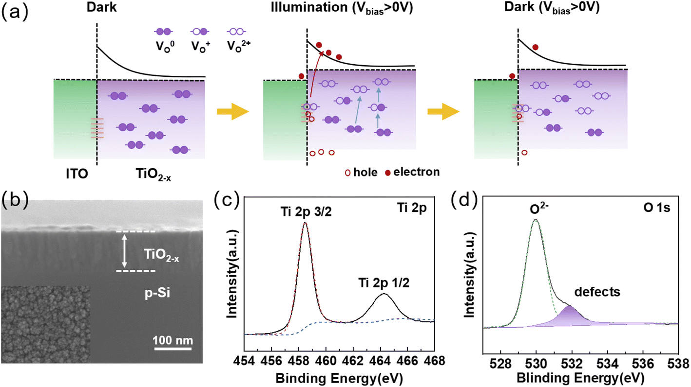 | ||
| Fig. 1 (a) Schematic operation mechanism of TiO2−x artificial optoelectronic synapse under dark and illumination conditions. (b) Cross-sectional and surface morphology image of TiO2−x films grown on p-Si substrate. (c) Ti 2p core level and (d) O 1s core level XPS spectrum of TiO2−x film. | ||
The surface topography information and cross-sectional of the TiO2−x thin films were examined by scanning electron microscope (SEM) (Fig. 1b). It can be seen from the surface topography that the grain size is small and the grains will form clusters. The thickness of the as-prepared TiO2−x film is ∼95 nm from the cross-sectional image, which is consistent with that measured in step-height image of AFM (Fig. S2a†). The roughness of ∼0.7 nm shown in the three-dimensional morphology (Fig. S2b†) illustrates the smoothness of the film surface. The XPS survey spectrum shown in Fig. S3† reveals that the samples mainly contain Ti, O, and C element. Fig. 1c shows the XPS spectra of Ti 2p. The Ti 2p peaks at 464.22 eV and 458.42 eV can be attributed to Ti 2p 1/2 and Ti 2p 3/2, respectively, which is consistent with the previous reports.40,41 The O1 peak can generally be decomposed into two sub-peaks at binding energy of 529.92 eV and 531.82 eV corresponding to lattice oxygen and non-lattice oxygen, respectively (Fig. 1d).42,43 The lower binding energy peak is attributed to Ti–O bonds, while the higher binding energy peak is associated with oxygen vacancies (defects). These defects play an important role in fabricated optoelectronic synaptic devices. Moreover, the XRD analysis images (Fig. S4†) also illustrate that the sample films have many defect states.
Humans acquire external information mainly through vision, so simulating the human visual system is crucial for the development of artificial intelligence. The synaptic transmission properties were mimicked on the proposed two-terminal optoelectronic synaptic devices more approximate to biological synapse structure.44,45 The TiO2−x optoelectronic synaptic devices were fabricated on a p-Si substrate, and top and bottom electrodes can be treated as the presynaptic and postsynaptic neurons, which are shown in Fig. 2a. Fig. 2b illustrated a typical light-induced excitatory postsynaptic current (EPSC) of the optoelectronic synaptic device under 1 V read voltage. The wavelength of the light pulse is 365 nm, and the intensity is 3.0 mW cm−2. More specifically, the value of EPSC is increased to 1.75 nA with an obvious current amplitude of ∼0.6 nA when the light is turned on for 3 s. The gradual decay property in EPSC (the fitted curve shown in Fig. S5†) indicates that short-term plasticity (STP) plays a central role in the realization of visual learning and memory.46 Paired-pulse facilitation (PPF) as a typical characteristic of STP reflects the capability of biological synapses for encoding temporal information in auditory and visual signals.47 The optoelectronic synaptic device exhibits an obvious PPF phenomenon as stimulated by two successive 365 nm light pulses with an interval time (Δt) of 2 s, which is shown in Fig. 2c. The amplitude of the EPSC inspired by the second pulse (A2) is significantly larger than the first one (A1). Furthermore, the PPF index is defined as 100% × (A2 − A1)/A1. Fig. 2d illustrates that the PPF index decreases with increasing pulse interval time, implying a gradual weakening of the effect between consecutive pulses. PPF index reaches a maximum of nearly 137% with an interval time of 2 s. The functional relationship of PPF index and interval time can be fitted with a biexponential function:48
| PPF = C1 exp(−t/τ1) + C2 exp(−t/τ2) | (1) |
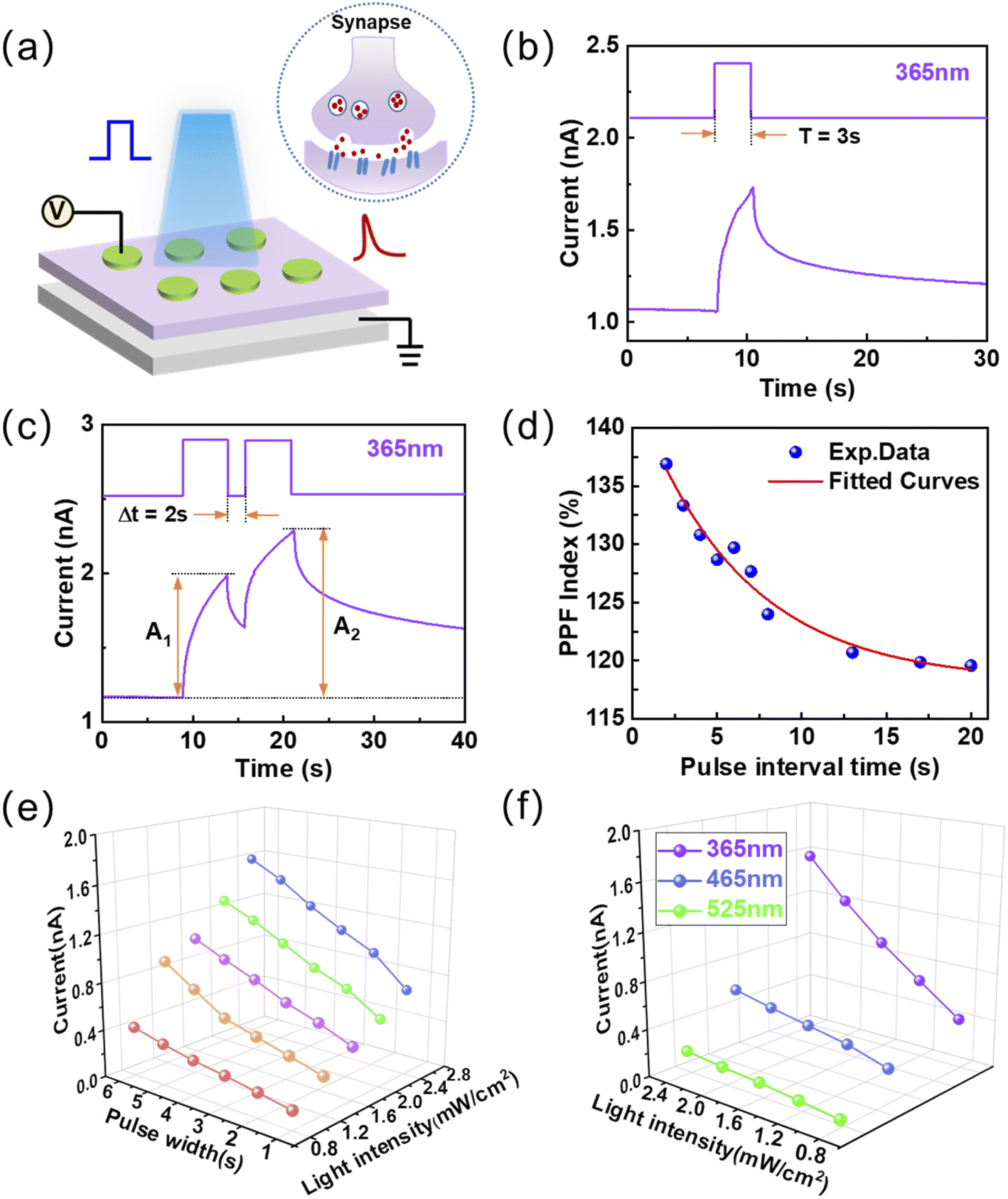 | ||
| Fig. 2 The basic short-term visual memory properties. (a) Schematic diagram of the prepared ITO/TiO2−x/p-Si devices and synapse structure. (b) EPSC triggered by a single light pulse of 365 nm with the intensity of 3.0 mW cm−2 (c) EPSCs triggered by two continuous light pulses with an interval time of 2 s. (d) PPF index varies with pulse interval time. (e) Current as a function of light intensity and light pulse width. (f) Current variation with light intensity and wavelength. | ||
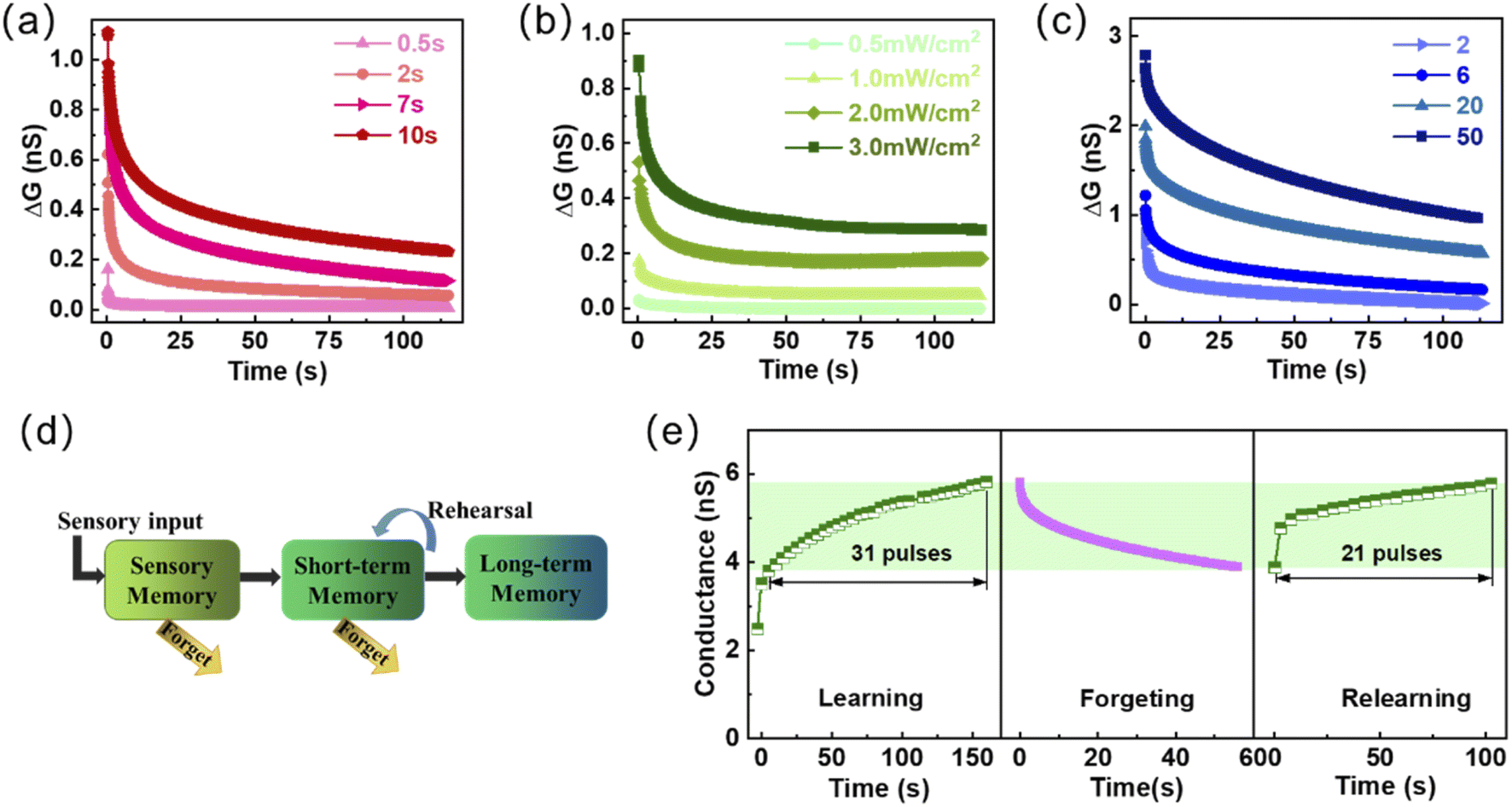
The important information in short-term memory (STM) is easily forgotten over time. While long-term memory (LTM) through continuous practice and stimulation is a state in which synaptic efficiency can be maintained for a long time, which is the basis for enhancing learning and memory ability.49,50 Fig. 3a shows the gradual increase in the level and the retention time of memory as the light width of the light pulse increases. The value of ΔG (ΔG = Glight − Gresting, Glight corresponds to the maximum conductance under light pulse and Gresting is the resting conductance in the dark state before the light pulse) increases from ∼0.18 nS to ∼1.5 nS when the optical pulse width increases from 0.5 s to 10 s. It is worth noting that the transition from STP to LTP can also be turned by modulating the light intensity and the number of light pulses, as shown in Fig. 3b and c, which can significantly enhance and consolidate visual learning and memory. Fig. 3d is a schematic diagram showing the biological multiple memory model in the human brain. The memory can be strengthened by enhancing or continuously repeating the input of external information stimulation, turning SM (Sensory memory) into STM and further into LTM.51 When learning new events, partial memory information will be gradually forgotten over time, as shown in Fig. 3e. The 31 light pulses were required to reach the conductance level of ∼5.8 nS from the conductance level of ∼3.8 nS, and this process takes 150 s. While, it only takes 21 light pulses to achieve the same conductance level when relearning from the same conductance lever of ∼3.8 nS, and the required time is reduced to 100 s. This phenomenon of conductance change illustrates the realization of the learning-forgetting-relearning process for external information on the proposed devices. This process is consistent with the Ebbinghaus forgetting curve, which describes the discipline of the human brain for forgetting new things.52
 | ||
| Fig. 3 Long-term memory simulated based on TiO2−x optoelectronic synaptic device by modulating the width (a), optical power density (b), and the number (c) of the light pulses. (d) The schematic diagram of the human brain “multiple memory”. (e) The “learning-forgetting-relearning” process mimicked on TiO2−x optoelectronic synaptic device. | ||
Human memory can be regulated and influenced by internal emotions and ambient illumination. Changes in memory are consistent with internal emotions. The higher the internal emotion, the higher the level of memory. The same goes for memory retention time. Furthermore, the brightness of the ambient illumination can also affect learning and memory ability. In this work, the memory levels and retention characteristics (response conductance) of the same event (input optical pulses information) under different internal emotion states (different bias voltages) and ambient illumination (different brightness) are mapped to images “H” identification (predefined into a 3 × 3 array). Seven optoelectronic synaptic devices were stimulated with light pulses to obtain response current. The other two optoelectronic synaptic devices were tested for response current without light stimulation. The detailed setting methods are shown in Fig. S6 and S10.† The fabricated optoelectronic devices exhibit excellent sensitivity to the event memory under different emotional states and different ambient illumination, which more realistically simulate the memory properties of human visual information.
The light intensity of the input optical pulse (event) information is 3.0 mW cm−2, the pulse width is 2 s, the pulse interval is 2 s, and the number of pulses is 8. The different internal emotion states are triggered by different biases, which are set to 0.5 V, 0.7 V, and 1.0 V, respectively. As shown in Fig. 4, the fabricated optoelectronic synaptic devices exhibit the behavior of internal emotions modulating visual memory. The visual memory based on relatively low emotion (resting conductance of ∼0.12 nS) at 0.5 V (Fig. 4a) was insufficient for “H” image recognition. The memory of the image almost disappears as the decay time increases to 200 s. The detailed current response curves were shown in Fig. S7.† As the bias voltage increases to 0.7 V, the value of the resting response conductance increases to ∼0.54 nS, indicating the raise of internal emotion (Fig. S8†). At the initial time, the image “H” can be recognized (Fig. 4d), but the image cannot be recognized as the decay time increases to 200 s (Fig. 4f). It is illustrated that insufficient emotional promotion has a weak effect on memory retention. While the response current can clearly identify the image “H” under relatively higher internal emotion with 1.0 V bias (Fig. 4g). The resting response conductance increases to ∼1.47 nS under 1.0 V bias (Fig. S9†). And memory similarly decays slowly as decay time increases. The response current still had an image-recognizable level at a decay time of 200 s under higher internal emotion (Fig. 4i). This phenomenon verifies the regulatory effect of internal emotion on visual memory.
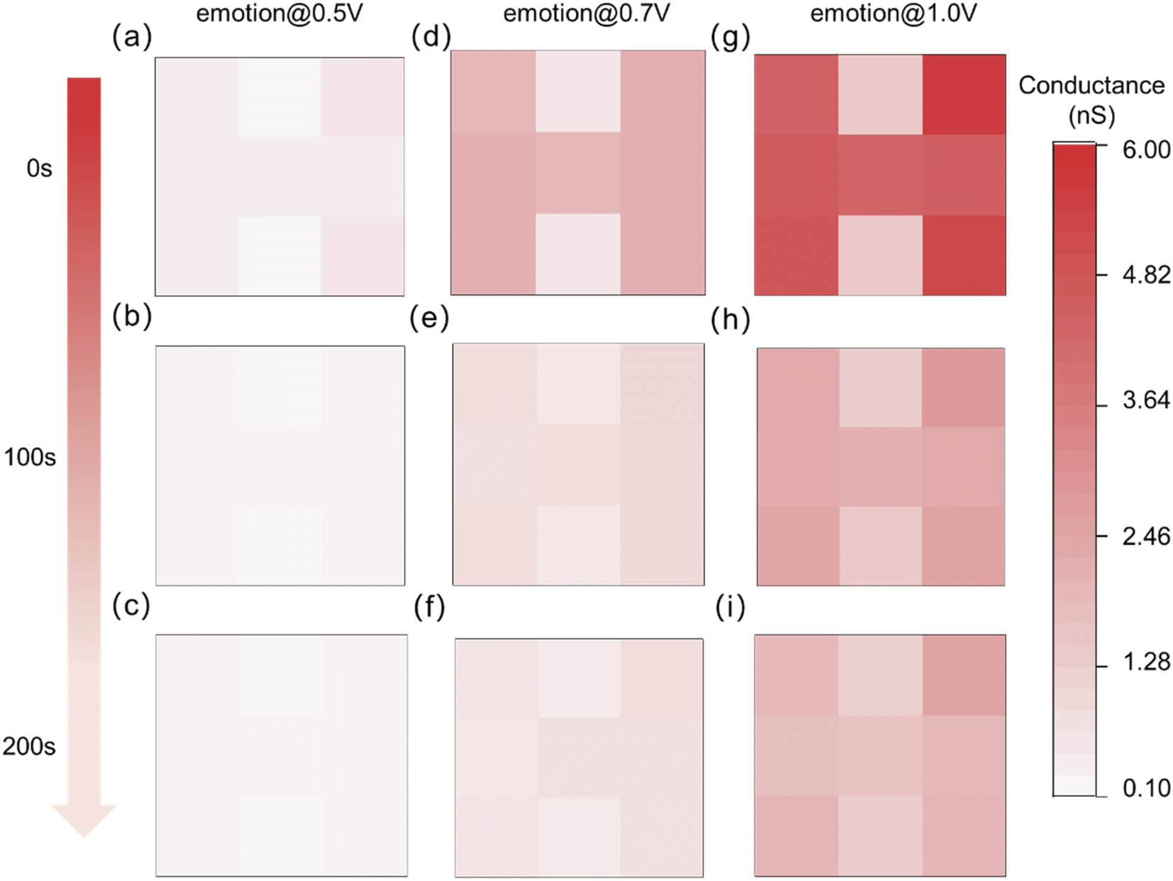 | ||
| Fig. 4 The change of visual memory of the optoelectronic synapse array with decay time at 0 s, 100 s and 200 s under three levers of internal emotions. | ||
Additionally, the level of visual memory can be affected by ambient illumination. The spectral distribution, brightness, and duration of ambient illumination have a certain degree of influence on memory and emotion. The regulation of ipRGCs on the individual non-visual effects is mainly accomplished by melanopsin, which has photosensitive properties. Studies have found that melanopsin is most sensitive to the blue light spectrum with wavelengths in the range of 460–480 nm.53,54 Therefore, a light source with a wavelength of 465 nm is adopted as ambient illumination in this paper. The same event was memorized after 20 s of ambient illumination. The proposed optoelectronic synaptic devices were in the same internal emotion. Fig. S10† shows the specific setting form in this process. As shown in Fig. 5a, d and g, the memory abilities for the same event were slightly improved with the increase of the brightness of the ambient illumination. While the memory retention ability is significantly enhanced with the ambient brightness (Fig. S11–S13†). The image “H” can still be distinctly recognizable when reaching the same forgetting time of 200 s. Obviously, the brighter the ambient illumination, the more pronounced the memory effect. In addition, the “H” image can be discernible at a decay time of 500 s with the light intensity of 4.0 mW cm−2, which clearly showed the characteristics of long-term memory (Fig. S14†). Ambient illumination has a non-visual effect on emotional states. The resting conductance, the emotional state, increases with the increasing brightness of the ambient illumination. At the same time, the maximum conductance triggered by the same event was also increased, indicating the enhancement of memory level. Moreover appropriately prolonging the duration time of ambient illumination can also enhance the level of memory-related proteins.55 The increase in resting response conductance and the maximum conductance under light pulses were observed on the optoelectronic synaptic device as the illumination duration increased from 5 s to 50 s (Fig. S15†). Thus, memory under lower emotions can be complemented by prolonged duration or enhanced brightness of the ambient illumination.
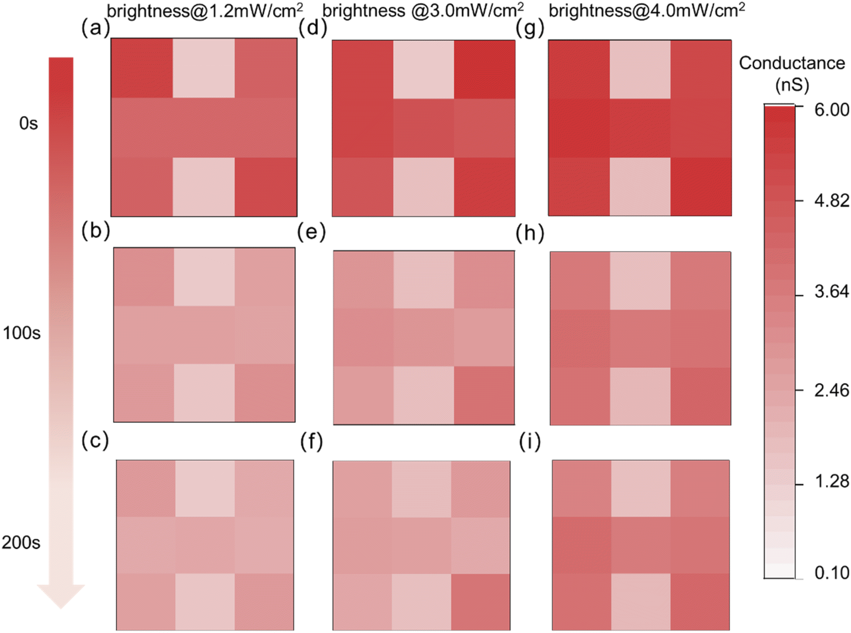 | ||
| Fig. 5 The change of visual memory of the optoelectronic synapse array with decay time at 0 s, 100 s and 200 s under different brightness of the ambient illumination. | ||
Human visual memory was realistically mimicked in a designed 3 × 3 optoelectronic synapse array by adjusting the level of internal emotions and the brightness of the ambient illumination. It shows that the memory level can be significantly affected by internal emotions, and the memory maintenance ability is relatively more affected by the brightness of the ambient illumination. This behavior effectively simulates superior visual perception and visual memory performance. A detailed comparison between previously reported photoelectronic artificial synapse devices and our ITO/TiO2−x/p-Si devices is provided in Table S1.† Herein, the image information detection and memory function that simulates the artificial visual system are achieved on our relatively simple device structure. More importantly, the effects of internal emotion and ambient illumination on visual perception and memory are discussed for the first time based on an optoelectronic synaptic array, which may lend it to a wider range of applications in complex conditions.
4. Conclusions
In conclusion, a single optoelectronic synaptic based on ITO/TIO2−x/p-Si device was successfully fabricated and demonstrated. The light-induced short-term synaptic plasticity of EPSC and PPF behaviors were simulated. The long-term synaptic plasticity transferred from short-term synaptic plasticity was demonstrated by adjusting the intensity, duration, and number of optical signal pulses. Based on excellent light perception and memory behavior, the high-level neural activity of learning-forgetting-relearning was realized. A 3 × 3 optoelectronic synapse array was constructed to reflect the effects of emotion and ambient illumination on visual learning and memory. It is a positive relationship between light memory and emotion or ambient illumination. The proposed artificial optoelectronic synapse offers a bright prospect for the realization of multifunctional electronic eye and artificial vision systems.Data availability
All data are fully available without restriction.Conflicts of interest
The authors declare that they have no competing interests.Acknowledgements
This work was supported by the National Natural Science Foundation of China (62111540271, 62104267, 61974090) and the Natural Science Foundation of Shanghai (19ZR1474500).References
- I. Boybat, L. M. Gallo and S. R. Nandakumar, Nat. Commun., 2018, 9, 2514 CrossRef PubMed
.
- P. A. Merolla, J. V. Arthur and R. Alvarez-Icaza, Science, 2014, 345, 668–673 CrossRef CAS
- M. M. Waldrop, Nature, 2016, 530, 144 CrossRef CAS PubMed
- E. Toomey, K. Segall, M. Castellani, M. Colangelo, N. Lynch and K. Berggen, Nano Lett., 2020, 20, 8059–8066 CrossRef CAS
- M. F. Bear and R. C. Malenka, Curr. Opin. Neurobiol., 1994, 4, 389–399 CrossRef CAS
- S. Kim, B. Choi, M. Lim, J. Yoon, J. Lee, H. D. Kim and S. J. Choi, ACS Nano, 2017, 11, 2814–2822 CrossRef CAS PubMed
- Y. Cao, X. Sha, X. Bai, Y. Shao, Y. Gao, Y. M. Wei, L. Meng, N. Zhou, J. Liu, B. Li, X. F. Yu and J. Li, Adv. Electron. Mater., 2022, 8, 2100902 CrossRef CAS
- F. Liao, Z. Zhou, B. J. Kim, J. Chen, J. Wang, T. Wan, Y. Zhou, A. T. Hoang, C. Wang, J. Kang, J. H. Ahn and Y. Chai, Nat. Electron., 2022, 5, 84–91 CrossRef
- F. Yu, J. C. Cai and L. Q. Zhu, ACS Appl. Mater. Interfaces, 2020, 12, 26258–26266 CrossRef CAS
- R. Kubota, Y. Sasaki, T. Minamiki and T. Minami, ACS Sens., 2019, 4, 2571–2587 CrossRef CAS
- M. Kumar, T. Som and J. Kim, Adv. Mater., 2019, 31, 1903095 CrossRef
- Q. B. Zhu, B. Li, D. D. Yang, C. Liu, S. Feng, M. L. Chen, Y. Sun, Y. N. Tian, X. Su, X. M. Wang, S. Qiu, Q. W. Li, X. M. Li, H. B. Zeng, H. M. Cheng and D. M. Sun, Nat. Commun., 2021, 12, 1798 CrossRef CAS PubMed
- H. Baier, Annu. Rev. Cell Dev. Biol., 2013, 29, 385–416 CrossRef CAS PubMed
- D. G. Seo, Y. Lee, G. T. Go, M. Pei, S. Jung, Y. H. Jeong, W. Lee, H. L. Park, S. W. Kim, H. Yang, C. Yang and T. W. Lee, Nano Energy, 2019, 65, 104035 CrossRef CAS
- S. Seo, S. H. Jo, S. Kim, J. Shim, S. Oh, J. H. Kim, K. Heo, J. W. Choi, C. Choi, S. Oh, D. Kuzum, H.-S. P. Wong and J. H. Park, Nat. Commun., 2018, 9, 5106 CrossRef PubMed
- H. Park, H. Kim, D. Lim, H. Zhou, Y. H. Kim, Y. Lee, S. Park and T. W. Lee, Adv. Mater., 2020, 32, 1906899 CrossRef CAS PubMed
- K. Nomura, H. Ohta, A. Takagi, T. Kamiya, M. Hirano and H. Hosono, Nature, 2004, 432, 488–492 CrossRef CAS
- J. Leppäniemi, O.-H. Huttunen, H. Majumdar and A. Alastalo, Adv. Mater., 2015, 27, 7168–7175 CrossRef PubMed
- J. W. Park, B. H. Kang and H. J. Kim, Adv. Funct. Mater., 2020, 30, 1904632 CrossRef CAS
- P. J. Whalen, S. L. Rauch, N. L. Etcoff, S. C. Mlcherney, M. B. Lee and M. A. Jenike, J. Neurosci., 1998, 18, 411–418 CrossRef CAS
- J. S. Morris, A. Ohman and R. J. Dolan, Nature, 1998, 393, 467–470 CrossRef CAS PubMed
- R. J. Dolan, Science, 2002, 298, 1191–19194 CrossRef CAS PubMed
- C. M. Tyng, H. U. Amin, M. N. M. Saad and A. S. Malik, Front. Psychol., 2017, 8, 1454 CrossRef PubMed
- B. R. Conway, Neuroscientist, 2009, 15, 274–290 CrossRef PubMed
- H. Zhu, N. Wang, L. Yao, Q. Chen, R. Zhang, J. Qian, Y. Hou, W. Guo, S. Fan, S. Liu, Q. Zhao, F. Du, X. Zuo, Y. Guo, Y. Xu, J. Li, T. Xue, K. Zhong, X. Song, G. Huang and W. Xiong, Cell, 2018, 173, 1716–1727 CrossRef CAS PubMed
- T. M. Brown, J. Wynne, H. D. Piggins and R. J. Lucas, J. Physiol., 2011, 589, 1173–1194 CrossRef CAS PubMed
- C. k. Adaikkan, S. J. Middleton, A. Marco, P. C. Pao, H. Mathys, D. N. Kim, F. Gao, J. Z. Young, H.-J. Suk, E. S. Boyden, T. J. McHugh and L. H. Tsai, Neurons, 2019, 102, 929–943 CrossRef CAS PubMed
- P. T. Stone, Light. Res. Technol., 1999, 31, 71–79 CrossRef
- T. A. LeGates, C. D. Fernandez and S. Hattar, Nat. Rev. Neurosci., 2014, 15, 443–454 CrossRef CAS
- A. Wirz-Justice, A. C. Schmid and P. Graw, Experientia, 1987, 43, 574–576 CrossRef CAS
- P. A. Crozier, M. R. McCartney and D. J. Smith, Surf. Sci., 1990, 237, 232 CrossRef CAS
- W. Zhang, J. Mao, W. K. Pang, X. Wang and Z. Guo, Nano Energy, 2018, 49, 549 CrossRef CAS
- H. Y. Liu, R. C. Huang, Y. Y. Li, C. S. Lee and W. C. Hsu, IEEE Electron. Device Lett., 2017, 38, 756 CAS
- D. Kim, Y. Kim, B. H. Kang, J. H. Lee, J. Chung and H. J. Kim, J. Mater. Chem. C, 2020, 8, 165–172 RSC
- S. Gao, G. Liu, H. Yang, C. Hu, Q. Chen, G. Gong, W. Xue, X. Yi, J. Shang and R. W. Li, ACS Nano, 2019, 13, 2634–2642 CrossRef CAS PubMed
- S. Song, M. Kim, G. Yoo, S. M. Kwon, J. S. Heo, S. K. Park and Y. H. Kim, J. Alloys Compd., 2021, 857, 158027 CrossRef CAS
- N. Duan, Y. Li, H. C. Chiang, J. Chen, W. Q. Pan, Y. X. Zhou, Y. C. Chien, Y. H. He, K. H. Xue, G. Liu, T. C. Chang and X. S. Miao, Nanoscale, 2019, 11, 17590–17599 RSC
- M. Lee, W. Lee, S. Choi, J. Jo, J. Kim, S. K. Park and Y. H. Kim, Adv. Mater., 2017, 29, 1700951 CrossRef
- J. J. Yu, L. Y. Liang, L. X. Hu, H. X. Duan, W. H. Wu, H. L. Zhang, J. H. Gao, F. Zhuge, T. C. Chang and H. T. Cao, Nano Energy, 2019, 62, 772–780 CrossRef CAS
- X. Yu, Y. Li, X. Hu, D. Zhang, Y. Tao, Z. Liu, Y. He, M. A. Haque, Z. Liu, T. Wu and Q. J. Wang, Nat. Commun., 2018, 9, 4299 CrossRef
- S. Nandi, R. Tripathi, G. D. Adhikary, P. Kumar and A. Misra, Adv. Mater. Interfaces, 2020, 7, 2001091 CrossRef CAS
- X. Yan, J. Zhao, S. Liu, Z. Zhou, Q. Liu, J. Chen and X. Y. Liu, Adv. Funct. Mater., 2018, 28, 1705320 CrossRef
- X. Y. Shan, Z. Q. Wang and Y. Lin, Adv. Electron. Mater., 2020, 6, 2000536 CrossRef CAS
- J. Kim, Y. Kim, O. Kwon, T. Kim, S. Oh, S. Jin, W. Park, J. D. Kwon, S. W. Hong, C. S. Lee, H. Y. Ryu, S. Hong, J. Kim, T. Y. Heo and B. Cho, Adv. Electron. Mater., 2020, 6, 1901072 CrossRef CAS
- Y. He, Y. Yang, S. Nie, R. Liu and Q. Wan, J. Mater. Chem. C, 2018, 6, 5336 RSC
- T. Ohno, T. Hasegawa, T. Tsuruoka, K. Terabe, J. K. Gimzewski and M. Aono, Nat. Mater., 2011, 10, 591–595 CrossRef CAS PubMed
- R. S. Zucker and W. G. Regehr, Annu. Rev. Physiol., 2002, 64, 355–405 CrossRef CAS
- W. Deng, X. J. Zhang, R. F. Jia, L. Huang, X. Zhang and J. Jie, NPG Asia Mater., 2019, 11, 77 CrossRef CAS
- S. J. Martin and R. G. Morris, Hippocampus, 2002, 12, 609–636 CrossRef CAS PubMed
- T. Takeuchi, A. J. Duszkiewicz and R. G. Morris, Philos. Trans. R. Soc., B, 2013, 369, 20130288 CrossRef PubMed
- R. C. Atkinson and R. M. Shiffrin, Psychol. Learn. Motiv., 1968, 2, 89–195 Search PubMed
- S. G. Hu, Y. Liu, T. P. Chen, Z. Liu, Q. Yu, L. J. Deng, Y. Yin and S. Hosaka, Appl. Phys. Lett., 2013, 103, 133701 CrossRef
- M. W. Hankins, S. N. Peirson and R. G. Foster, Trends Neurosci., 2008, 31, 27–36 CrossRef CAS PubMed
- D. M. Dacey, H. W. Liao, B. B. Peterson, F. R. Robinson, V. C. Smith, J. Pokorny, K. W. Yau and P. D. Gamlin, Nature, 2005, 433, 749–754 CrossRef CAS PubMed
- C. Li, W. Du, H. Liu, M. Yang, H. Xu, J. Wu and Z. Wang, Sci. China Mater., 2022, 65, 1087–1093 CrossRef
Footnote |
| † Electronic supplementary information (ESI) available. See https://doi.org/10.1039/d2ra02749f |
| This journal is © The Royal Society of Chemistry 2022 |