
 Open Access Article
 This Open Access Article is licensed under a Creative Commons Attribution-Non Commercial 3.0 Unported Licence
Electronic structure and interface contact of two-dimensional van der Waals boron phosphide/Ga2SSe heterostructures†
Hoang-Thinh Doab,
Tuan V. Vu c,
A. A. Lavrentyevd,
Nguyen Q. Cuongef,
Pham V. Cuongg and
Hien D. Tong*h
c,
A. A. Lavrentyevd,
Nguyen Q. Cuongef,
Pham V. Cuongg and
Hien D. Tong*h
aDivision of Computational Mechatronics, Institute for Computational Science, Ton Duc Thang University, Ho Chi Minh City, Vietnam. E-mail: dohoangthinh@tdtu.edu.vn
bFaculty of Electrical and Electronics Engineering, Ton Duc Thang University, Ho Chi Minh City, Vietnam
cDivision of Computational Physics, Institute for Computational Science, Ton Duc Thang University, Ho Chi Minh City, Vietnam
dDepartment of Electrical Engineering and Electronics, Don State Technical University, 1 Gagarin Square, 344010 Rostov-on-Don, Russian Federation
eInstitute of Research and Development, Duy Tan University, Da Nang 550000, Vietnam
fFaculty of Natural Sciences, Duy Tan University, Da Nang 550000, Vietnam
gFaculty of Electrical Engineering Technology, Ha Noi University of Industry, Ha Noi 100000, Vietnam
hFaculty of Engineering, Vietnamese-German University, Binh Duong, Vietnam. E-mail: hien.td@vgu.edu.vn
First published on 30th June 2022
Abstract
In this work, we systematically examine the electronic features and contact types of van der Waals heterostructures (vdWHs) combining single-layer boron phosphide (BP) and Janus Ga2SSe using first-principles calculations. Owing to the out-of-plane symmetry being broken, the BP/Ga2SSe vdWHs are divided into two different stacking patterns, which are BP/SGa2Se and BP/SeGa2S. Our results demonstrate that these stacking patterns are structurally and mechanically stable. The combination of single-layer BP and Janus Ga2SSe gives rise to an enhancement in the Young’s modulus compared to the constituent monolayers. Furthermore, at the ground state, the BP/Ga2SSe vdWHs possess a type-I (straddling) band alignment, which is desired for next-generation optoelectronic applications. The interlayer separation and electric field are effectively used to tune the electronic features of the BP/Ga2SSe vdWH from the type-I to type-II band alignment, and from semiconductor to metal. Our findings show that the BP/Ga2SSe vdWH would be appropriate for next-generation multifunctional optoelectronic and photovoltaic devices.
1 Introduction
In recent years, the search for novel materials has attracted much attention because of their unusual physical and chemical properties, which are appropriate for future high-performance nanoelectronic and optoelectronic devices. Recently, novel two-dimensional materials (2DMs) have appeared as promising candidates for novel optoelectronic and photocatalytic applications, owing to their extraordinary electronic properties and suitable band gaps.1,2 At first, one of the most popular 2DMs, graphene, was successfully exfoliated3 and received much attention owing to its high carrier mobility4 and massive Dirac fermions.5 Unfortunately, the lack of a band gap in graphene has limited its applications in high-speed devices, such as logical circuits and field-effect transistors.6 Recently, there have been different strategies that can be used to open a sizable band gap in graphene, such as doping,7 functionalization,8 use of substrates,9 and so on. Alongside these strategies, scientists are seeking novel graphene-like 2DMs, such as phosphorene,10 transition metal dichalcogenides (TMDCs),11 MXenes,12,13 and so on. Unlike graphene, these 2DMs mostly possess semiconducting characteristics, thus they are suitable for optoelectronic and photocatalytic applications. Regarding the promising unique properties of 2DMs, the search for novel 2DMs remains challenging.Very recently, single-layer boron phosphide (BP) has been successfully synthesized on sapphire or silicon substrates14,15 and its properties predicted using different theoretical calculations.16,17 It is obvious that single-layer BP is a semiconductor with a direct band gap of about 1.0–2.0 eV, depending on the measurement approaches.18,19 Single-layer BP shows high carrier mobilities (over 104 cm2 V−1 s−1),20 which are comparable with those in graphene (105 cm2 V−1 s−1).21 The electronic, magnetic and transport properties of single-layer BP can be modulated by doping22,23 and applying an electric field.24 These controllable characteristics make single-layer BP a promising competitor for future applications.
Following the successful synthesis of a Janus MoSSe structure from MoS2 and MoSe2 monolayers,25,26 many different 2D Janus structures have also been predicted and synthesized, including Janus ZrSSe,27 Janus PtSSe,28,29 Janus Pd4S3Se330 and Janus group-III chalcogenides.31,32 The superior properties of Janus structures are due to the out-of-plane symmetry being broken. 2D Ga2SSe – a member of the Janus group-III chalcogenides – has been predicted to be mechanically and thermodynamically stable at room temperature.31,32 The electronic and optical properties of Janus Ga2SSe are dependent on the number of layers,33 atomic adsorption,34 and so on.
Currently, making van der Waals heterostructures (vdWHs) from two or more 2DMs is widely used to generate novel properties that may not exist in single-layer forms. Many vdWHs have been constructed and investigated, including the vdWHs based on single-layer BP,35–38 and based on Janus Ga2SSe.39–41 The combination of two or more different semiconducting 2DMs is divided into three different band alignments, including type-I (straddling), type-II (staggered) and type-III (broken). Furthermore, these combinations also lead to an increase in the optical absorption of the constituent 2DMs. With these promising properties, vdWHs are promising competitors for high-performance optoelectronic and photocatalytic applications.42–44 To date, the combination of single-layer BP and Janus Ga2SSe monolayers has not yet been constructed and investigated. In this study, we systematically examine the electronic features of BP/Ga2SSe vdWHs. The influences of the interlayer separations and electric field are also discussed and evaluated. Our findings demonstrated that the BP/Ga2SSe vdWHs are promising competitors for next-generation multifunctional optoelectronic and photovoltaic devices.
2 Computational methods
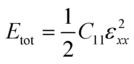
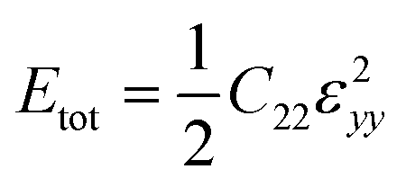
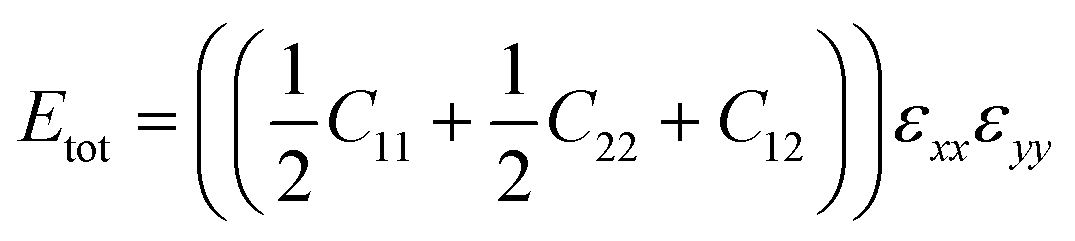
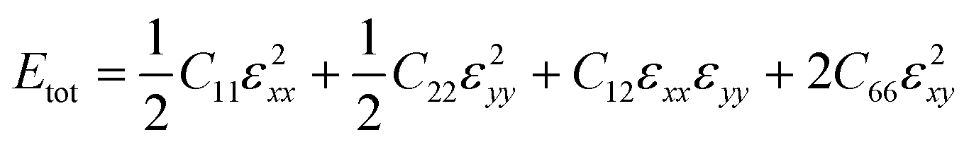
All the calculations were based on first-principles calculations and were performed in the Vienna ab initio simulation package (VASP).45 The projector augmented wave (PAW) method46 with the Perdew-Burke-Ernzerhofer (PBE) functional was used for describing the electron–ion interactions. Moreover, there have been different approaches that described correctly the electron–ion interactions, such as PBEsol47 and HLE17.48 The weak vdW interactions in vdWHs were described by adding the Grimme correction in the DFT-D2 method.49 To avoid the unnecessary interactions, a vacuum thickness of 40 Å was adopted along the z direction of the vdWHs. All atomic structures were fully relaxed until the energy was less than 10−6 eV and the forces less than 10−3 eV Å−1. The cutoff energy was chosen to be 510 eV and the (11 × 11 × 1) k-point meshes were used for the Brillouin zone. The charge density difference in the considered heterostructures was visualized using the VESTA software package.50 The elastic constants of the considered systems were obtained from the curvature of the energy–strain relationship51 with suitable sets of deformations in each unit cell. The in-plane elastic constants [Cij] of the materials can be obtained from a stress–strain approach that is based on Hooke’s law:52| {δij} = [Cij]{εij} | (1) |
 | (2) |
and
 | (3) |
 | (4) |
Finally, when the biaxial strain εxy is applied, we calculated the elastic constant C66 as follows:
 | (5) |
3 Results and discussion
Fig. 1 illustrates the structure of the combination of BP and Ga2SSe monolayers. The BP/Ga2SSe heterostructure forms two main stacking patterns of BP/SGa2Se and BP/SeGa2S due to the broken vertical symmetry. In the first stacking pattern, the BP layer is stacked on the S layer of the Ga2SSe layer. Whereas, in the other stacking pattern, the BP is stacked on top of the Se layer of the Ga2SSe layer. The optimized interlayer separation between BP and Ga2SSe layers is 3.28 and 3.32 Å for the first and second stacking patterns, respectively. These values of interlayer separation are in the same order of magnitude as those of other BP-based vdWHs,35,36,38,53 suggesting that the two main stacking patterns of BP/Ga2SSe vdWHs are typical vdW systems. The binding energy is also taken into account to provide information on the stability of the vdWHs as follows: Eb = [EvdWH − (EBP + EGa2SSe)]/A, where EvdWH, EBP and EGa2SSe are the total energies of the vdWH, BP and Ga2SSe layers, respectively. A is the surface area of the heterostructure. The evaluated Eb of BP/SGa2Se and BP/SeGa2S vdWHs is −35.24 and −23.75 meV Å−2, respectively. The negative values of Eb suggest that both of these vdWHs are energetically stable. Furthermore, these values of the binding energy of the vdWHs suggest that they are characterized mainly by weak vdW interactions instead of strong covalent bonds. The weak vdW interactions keep the heterostructures feasible and possible to realize experimentally.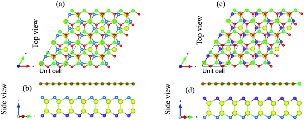 | ||
| Fig. 1 The optimized atomic structures of (a and b) BP/SGa2Se and (c and d) BP/SeGa2S vdWHs. Green and red balls represent the B and P atoms in the BP layer, respectively, while cyan, yellow and violet balls represent the S, Ga and Se atoms in the Janus Ga2SSe layer, respectively. | ||
The orbital projected band structures (OPBS) of the BP/Ga2SSe vdWHs for the two stacking patterns are displayed in Fig. 2. One can firstly observe that both stacking patterns of the BP/Ga2SSe vdWH are semiconductors with direct band gaps. The minimum of the conduction bands (MCB) and the maximum of the valence bands (MVB) are located at the M point. More interestingly, both the MCB and MVB of the BP/Ga2SSe vdWHs for the two stacking patterns originate from the BP layer, which gives rise to formation of the type-I (straddling) band alignment. This finding indicates that the BP/Ga2SSe vdWH is a suitable material for optoelectronic devices. Furthermore, the band gaps of the BP/SGa2Se and BP/SeGa2S vdWHs are about 0.85 eV, which are suitable band gaps for water splitting applications.
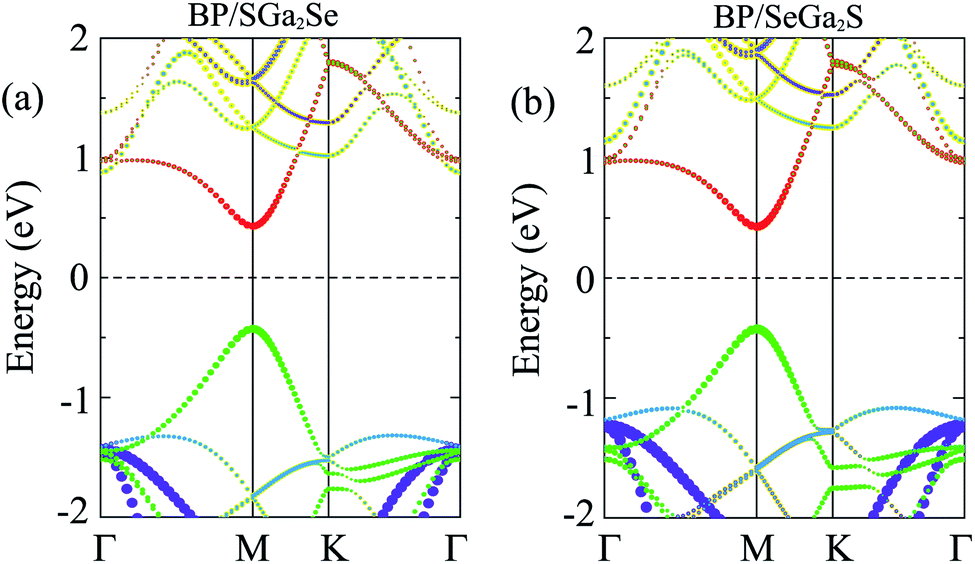 | ||
| Fig. 2 Orbital projected band structures of the (a) BP/SGa2Se and (b) BP/SeGa2S vdWHs. Red and green circles represent the contributions of boron and phosphorus in the BP layer, respectively. Yellow, blue and violet circles represent the contributions of gallium, sulfur and selenium atoms in the Ga2SSe layer, respectively. | ||
The planar-averaged and 3D charge density differences (CDD) are also visualized and displayed in Fig. 3(a) and (b). The CDD can be obtained by the differences between the charge density of the vdWH (ρvdWH) and those of isolated BP (ρBP) and Ga2SSe (ρGa2SSe) as: Δρ = ρvdWH − (ρBP + ρGa2SSe). The negative sign suggests that the charges are depleted, while the positive sign indicates the charge accumulation. From Fig. 3, the charges are mainly visualized at the interface between the BP layer and the topmost S (Se) layer of the Ga2SSe layer in their corresponding vdWH. In addition, one can observe that the BP layer gains electrons, while the Ga2SSe layer donates electrons. Bader charge analysis54–56 is used to calculate the charge transfers between the two layers in the corresponding vdWHs. The calculated amount of charge transferred between the BP and Ga2SSe layers in their combined vdWHs is about 0.014 e, as depicted in Fig. 3(a and b). The electrostatic potential of the BP/Ga2SSe vdWH for different stacking patterns is illustrated in Fig. 3(c and d). We observe that the BP layer has a deeper potential than that of the Ga2SSe layer, indicating that the electrons are transferred from Ga2SSe to the BP layer.
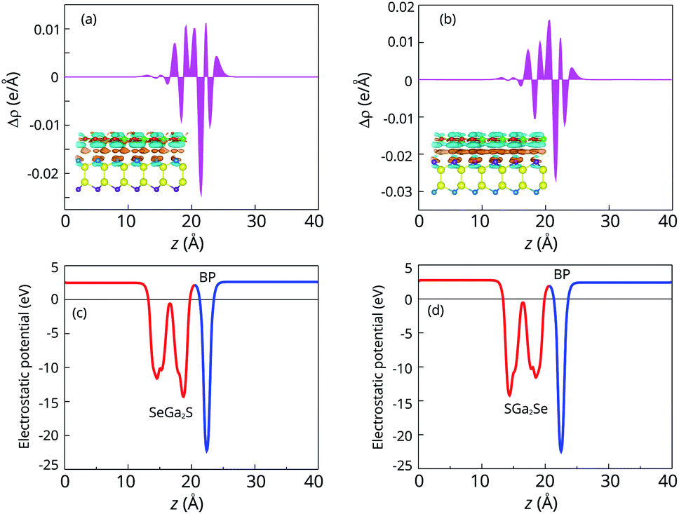 | ||
| Fig. 3 The planar-averaged charge density difference of the (a) BP/SGa2Se and (b) BP/SeGa2S vdWHs. The insets represent the 3D charge density difference. Orange and cyan regions represent the charge accumulation and depletion, respectively. The isosurface value is set to 0.0025 e Å−3. The electrostatic potential of the (c) BP/SGa2Se and (d) BP/SeGa2S heterostructures. | ||
Elastic properties play a crucial role in describing information about the structural stability of any material. We now go on to evaluate the mechanical stability of such systems by calculating their elastic constants, Young’s modulus and Poisson’s ratio. As we have discussed above, both the BP/SGa2Se and BP/SeGa2S vdWHs have layered hexagonal structures. Thus, from eqn (1), there are four independent elastic constants, Cij, of the BP/Ga2SSe vdWHs, including C11, C22, C12 and C66. The measured elastic constants of the BP/Ga2SSe vdWHs are C11 = C22 = 233.30 N m−1, C12 = 61.50 N m−1 and C66 = (C11 − C12)/2 = 86 N m−1. It is clear that these values of the elastic constants meet the Born criteria,57,58 thus suggesting that the BP/Ga2SSe vdWHs are mechanically stable. Furthermore, the orientation dependence of Young’s modulus and Poisson’s ratio of the BP/Ga2SSe vdWHs is calculated and plotted in Fig. 4. One can find that the Young’s modulus and Poisson’s ratio of the BP/Ga2SSe vdWHs for different stacking patterns are about 210 N m−1 and 0.25, respectively. One can find that the Young’s modulus of the BP/Ga2SSe vdWHs is still higher than that of single-layer BP,59 suggesting that the combination of the BP and Ga2SSe layers gives rise to an enhancement of the Young’s modulus.
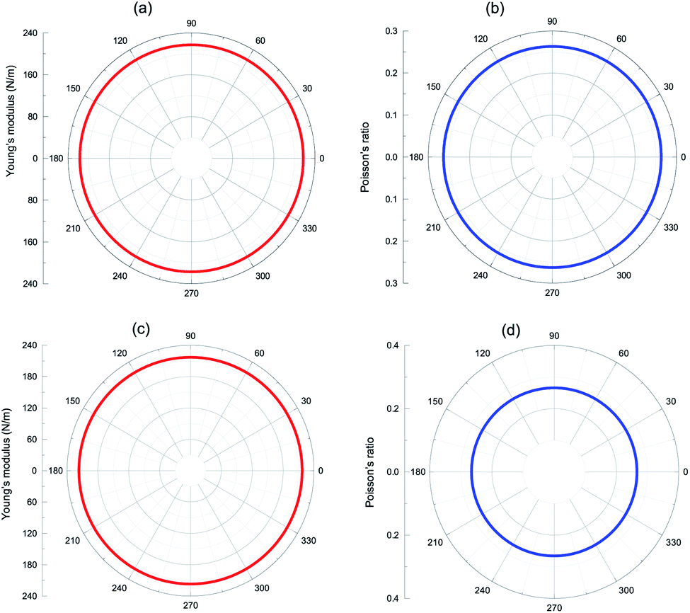 | ||
| Fig. 4 Polar plots of (a and c) Young’s modulus and (b and d) Poisson’s ratio of the (a and b) BP/SGa2Se and (c and d) BP/SeGa2S stacking patterns. | ||
More interestingly, the electronic and interface characteristics of 2D vdWHs can be modulated by controlling the interlayer separation and applying an electric field.60–62 We thus consider their influences on the electronic features of the most energetically favorable stacking pattern of the BP/Ga2SSe vdWHs. The schematic models of the electric field and strain applied to the vdWH are displayed in Fig. S1 of the ESI.† The influence of the electric field (Eext) on the electronic features of the BP/SGa2Se stacking pattern is displayed in Fig. 5(a). Under the negative neg-Eext, the MVB of the BP and Ga2SSe layers shifts in opposite directions. The MVB of the BP layer comes to the Fermi level (EF), while the MVB of the Ga2SSe layer shifts far from the EF. At the same time, the MCB of the BP and Ga2SSe layers also moves in different directions. The MCB of the BP layer shifts far from the EF, whereas the MCB of the Ga2SSe layer comes towards the EF. Owing to these movements, at the critical strength of neg-Eext = −0.40 V nm−1, the MCB of the Ga2SSe layer moves closer to the EF than that of the BP layer. In this case, the MCB of the BP/Ga2SSe vdWH originates from the Ga2SSe layer, while the MVB is preserved by the contribution of the BP layer, thus revealing the conversion from a type-I to type-II (staggered) band alignment. It is obvious that the type-II band alignment reduces the recombination of electron–hole pairs, revealing that the BP/Ga2SSe vdWH is beneficial for photovoltaic devices. The influence of the positive pos-Eext on the electronic features of the BP/Ga2SSe vdWH is illustrated in Fig. 5(b). One can observe that the MVB of the Ga2SSe layer tends to shift towards the EF. At the same time, the MVB of the BP layer is shifted closer to the EF. At the critical strength of pos-Eext = +0.40 V nm−1, the MVB of the BP layer touches the EF. Furthermore, when pos-Eext is further increased to +0.5 V nm−1, the MVB of the BP layer crosses the Fermi level, resulting in the transformation from semiconductor to metal, as depicted in Fig. S2 of the ESI.† All of the above-discussed findings indicate that Eext gives rise to the conversion from type-I to type-II band alignment and the transformation from semiconductor to metal in the BP/Ga2SSe vdWH.
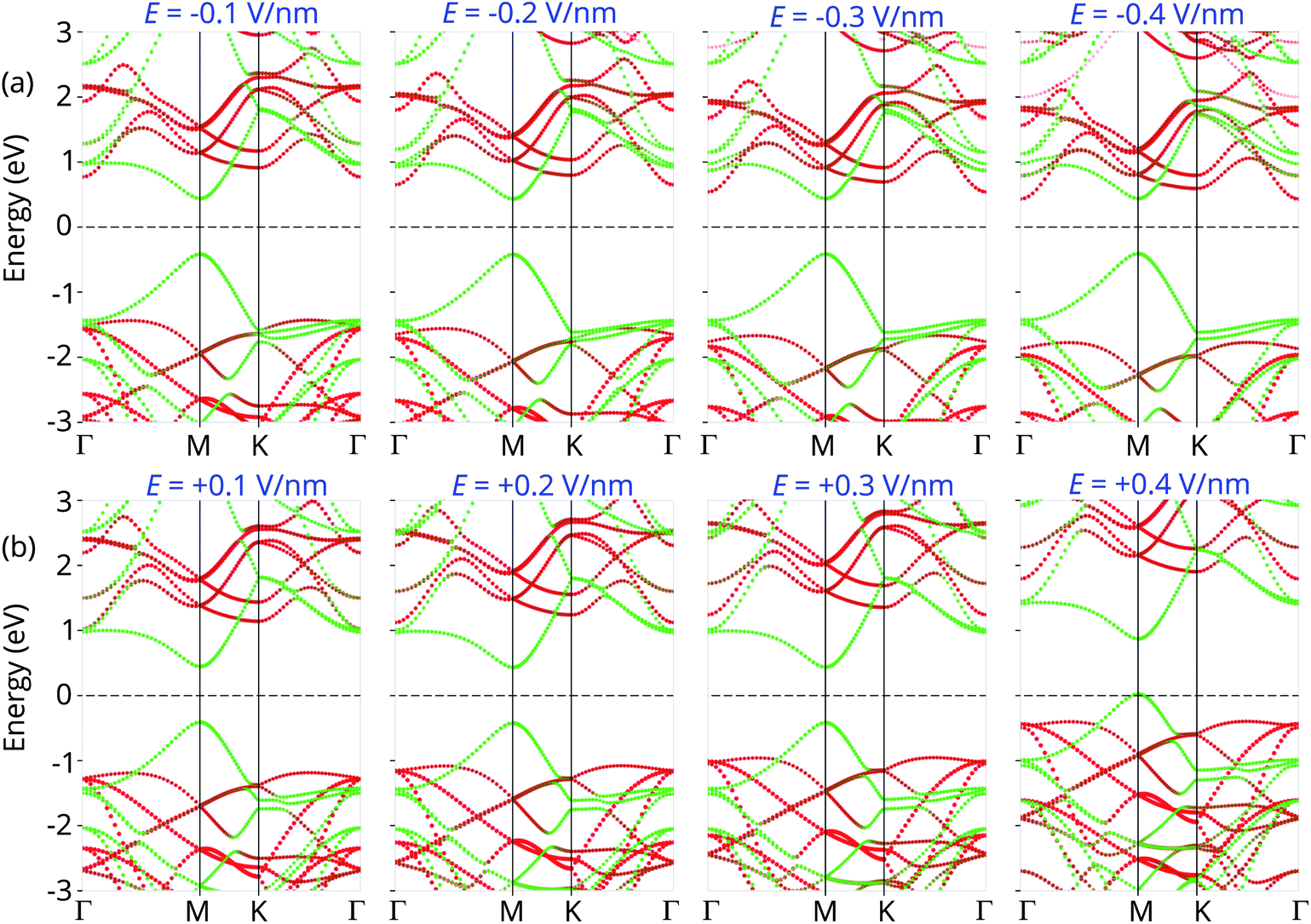 | ||
| Fig. 5 Projected band structures of the BP/SGa2Se vdWH under (a) negative and (b) positive electric fields. Green and red lines represent the contributions of the BP and Ga2SSe layers, respectively. The Fermi level is set to be zero and defined by the dashed line. | ||
The influence of the interlayer separation on the electronic features of the BP/Ga2SSe vdWH is illustrated in Fig. 6. The change of the interlayer separation is defined as ΔD = D0 −D, where D0 and D represent the interlayer separation of the BP/Ga2SSe vdWH in the equilibrium state and strained state, respectively. Under the compressive separation, i.e. ΔD < 0, as depicted in Fig. 6(a), it tends to a reduction of the band gap of the BP/Ga2SSe vdWH. The band gap of the BP/Ga2SSe vdWH reduces from 0.85 eV at ΔD = 0 to 0.67 and 0.45 eV at ΔD = −0.8 Å and −1.2 Å, respectively. The BP/Ga2SSe vdWH at ΔD < 0 maintains the type-I band alignment with both the MCB and MVB originating from the BP layer. At ΔD = −1.6 Å, both the MVB and MCB of the BP layer in the BP/Ga2SSe vdWH touch the EF. In particular, at ΔD = −1.7 Å, as depicted in Fig. S2 of the ESI,† both the MVB and MCB of the heterostructure cross the Fermi level, suggesting that the BP/Ga2SSe vdWH turns into a metal. Whereas with an increase of the interlayer separation, i.e. ΔD > 0, the band edges of both the BP and Ga2SSe layers in the BP/Ga2SSe vdWH are almost unchanged in comparison with the position of the EF. This finding indicates that the BP/Ga2SSe vdWH keeps the type-I band alignment with the contributions of the BP layer in both the MVB and MCB.
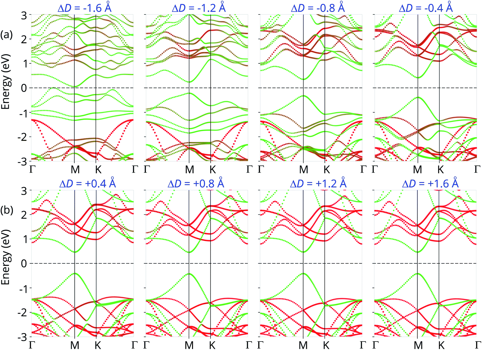 | ||
| Fig. 6 Projected band structures of the BP/SGa2Se heterostructure under (a) compressive and (b) tensile strains. Green and red lines represent the contributions of the BP and Ga2SSe layers, respectively. The Fermi level is set to be zero and defined by the dashed line. | ||
4 Conclusions
In summary, we have investigated the electronic structure and interface characteristics of vdWHs combining single-layer BP and Janus Ga2SSe using first-principles calculations. Owing to the out-of-plane symmetry being broken in the Janus Ga2SSe layer, the BP/Ga2SSe vdWHs form two different stacking patterns, BP/SGa2Se and BP/SeGa2S. Both these stacking patterns are energetically and mechanically stable, confirming that they can be obtained experimentally. Moreover, the combination of single-layer BP and Janus Ga2SSe tends to an enhancement of the elastic constants, as well as the Young’s modulus, compared to the constituent monolayers. The BP/Ga2SSe vdWHs for the two stacking patterns exhibit type-I band alignment with both the MVB and MCB originating from the BP layer. Interestingly, we found that the electronic structure and contact types of the BP/Ga2SSe vdWHs are dependent on the interlayer separation and electric field, giving rise to the conversion from type-I to type-II band alignment, and from semiconductor to metal. Our results indicate that the BP/Ga2SSe vdWH would be appropriate for next-generation multifunctional optoelectronic and photovoltaic devices.Conflicts of interest
There are no conflicts to declare.References
- S. Z. Butler, S. M. Hollen, L. Cao, Y. Cui, J. A. Gupta, H. R. Gutiérrez, T. F. Heinz, S. S. Hong, J. Huang, A. F. Ismach, E. Johnston-Halperin, M. Kuno, V. V. Plashnitsa, R. D. Robinson, R. S. Ruoff, S. Salahuddin, J. Shan, L. Shio, M. G. Spencer, M. Terrones, W. Windl and J. E. Goldberger, ACS Nano, 2013, 7, 2898–2926 CrossRef CAS PubMed.
- P. Miró, M. Audiffred and T. Heine, Chem. Soc. Rev., 2014, 43, 6537–6554 RSC.
- K. S. Novoselov, A. K. Geim, S. V. Morozov, D.-e. Jiang, Y. Zhang, S. V. Dubonos, I. V. Grigorieva and A. A. Firsov, Science, 2004, 306, 666–669 CrossRef CAS PubMed.
- X. Du, I. Skachko, A. Barker and E. Y. Andrei, Nat. Nanotechnol., 2008, 3, 491–495 CrossRef CAS.
- K. S. Novoselov, A. K. Geim, S. V. Morozov, D. Jiang, M. I. Katsnelson, I. Grigorieva, S. Dubonos and a. Firsov, Nature, 2005, 438, 197–200 CrossRef CAS PubMed.
- D. Reddy, L. F. Register, G. D. Carpenter and S. K. Banerjee, J. Phys. D: Appl. Phys., 2011, 44, 313001 CrossRef.
- T. Wehling, K. Novoselov, S. Morozov, E. Vdovin, M. Katsnelson, A. Geim and A. Lichtenstein, Nano Lett., 2008, 8, 173–177 CrossRef CAS.
- T. Kuila, S. Bose, A. K. Mishra, P. Khanra, N. H. Kim and J. H. Lee, Prog. Mater. Sci., 2012, 57, 1061–1105 CrossRef CAS.
- S. Y. Zhou, G.-H. Gweon, A. Fedorov, P. N. First, W. De Heer, D.-H. Lee, F. Guinea, A. Castro Neto and A. Lanzara, Nat. Mater., 2007, 6, 770–775 CrossRef CAS.
- A. Carvalho, M. Wang, X. Zhu, A. S. Rodin, H. Su and A. H. Castro Neto, Nat. Rev. Mater., 2016, 1, 16061 CrossRef CAS.
- S. Manzeli, D. Ovchinnikov, D. Pasquier, O. V. Yazyev and A. Kis, Nat. Rev. Mater., 2017, 2, 17033 CrossRef CAS.
- Y. Gogotsi and B. Anasori, The rise of MXenes, 2019 Search PubMed.
- M. Khazaei, A. Mishra, N. S. Venkataramanan, A. K. Singh and S. Yunoki, Curr. Opin. Solid State Mater. Sci., 2019, 23, 164–178 CrossRef CAS.
- Y. Kumashiro, K. Nakamura, T. Enomoto and M. Tanaka, J. Mater. Sci.: Mater. Electron., 2011, 22, 966–973 CrossRef CAS.
- K. Shohno, M. Takigawa and T. Nakada, J. Cryst. Growth, 1974, 24–25, 193–196 CrossRef CAS.
- Y. Wang, C. Huang, D. Li, P. Li, J. Yu, Y. Zhang and J. Xu, J. Phys.: Condens. Matter, 2019, 31, 285501 CrossRef CAS.
- Y. Wang, C. Huang, D. Li, F. Huang, X. Zhang, K. Huang and J. Xu, J. Phys.: Condens. Matter, 2019, 31, 465502 CrossRef CAS.
- H. Şahin, S. Cahangirov, M. Topsakal, E. Bekaroglu, E. Akturk, R. T. Senger and S. Ciraci, Phys. Rev. B: Condens. Matter Mater. Phys., 2009, 80, 155453 CrossRef.
- R. Zhang, F. Sun, Z. Zhang, J. Liu, Y. Tian, Y. Zhang, X. Wei, T. Guo, J. Fan and L. Ni, et al., Appl. Surf. Sci., 2021, 535, 147825 CrossRef CAS.
- M. Xie, S. Zhang, B. Cai, Z. Zhu, Y. Zou and H. Zeng, Nanoscale, 2016, 8, 13407–13413 RSC.
- K. I. Bolotin, K. J. Sikes, Z. Jiang, M. Klima, G. Fudenberg, J. Hone, P. Kim and H. Stormer, Solid State Commun., 2008, 146, 351–355 CrossRef CAS.
- M. M. Obeid, H. R. Jappor, K. Al-Marzoki, D. Hoat, T. V. Vu, S. J. Edrees, Z. M. Yaseen and M. M. Shukur, Comput. Mater. Sci., 2019, 170, 109201 CrossRef CAS.
- B. Onat, L. Hallioglu, S. Ipek and E. Durgun, J. Phys. Chem. C, 2017, 121, 4583–4592 CrossRef CAS.
- M. Yarmohammadi and K. Mirabbaszadeh, J. Appl. Phys., 2020, 128, 215703 CrossRef CAS.
- J. Zhang, S. Jia, I. Kholmanov, L. Dong, D. Er, W. Chen, H. Guo, Z. Jin, V. B. Shenoy and L. Shi, et al., ACS Nano, 2017, 11, 8192–8198 CrossRef CAS PubMed.
- A.-Y. Lu, H. Zhu, J. Xiao, C.-P. Chuu, Y. Han, M.-H. Chiu, C.-C. Cheng, C.-W. Yang, K.-H. Wei and Y. Yang, et al., Nat. Nanotechnol., 2017, 12, 744–749 CrossRef CAS.
- S.-D. Guo, Y.-F. Li and X.-S. Guo, Comput. Mater. Sci., 2019, 161, 16–23 CrossRef CAS.
- R. Peng, Y. Ma, B. Huang and Y. Dai, J. Mater. Chem. A, 2019, 7, 603–610 RSC.
- X. Gao, Y. Shen, J. Liu, L. Lv, M. Zhou, Z. Zhou, Y. P. Feng and L. Shen, J. Mater. Chem. C, 2021, 9, 15026–15033 RSC.
- Y. Luo, M. Sun, J. Yu and U. Schwingenschlogl, Chem. Mater., 2021, 33, 4128–4134 CrossRef CAS.
- R. da Silva, R. Barbosa, R. R. Mancano, N. Duraes, R. B. Pontes, R. Miwa, A. Fazzio and J. E. Padilha, ACS Appl. Nano Mater., 2019, 2, 890–897 CrossRef CAS.
- Y. Guo, S. Zhou, Y. Bai and J. Zhao, Appl. Phys. Lett., 2017, 110, 163102 CrossRef.
- A. Huang, W. Shi and Z. Wang, J. Phys. Chem. C, 2019, 123, 11388–11396 CrossRef CAS.
- S. Singh and S. Choudhary, Opt. Quantum Electron., 2021, 53, 1–13 CrossRef.
- C. Nguyen, N. V. Hoang, H. V. Phuc, A. Y. Sin and C. V. Nguyen, J. Phys. Chem. Lett., 2021, 12, 5076–5084 CrossRef CAS PubMed.
- I. Shahid, S. Ahmad, N. Shehzad, S. Yao, C. V. Nguyen, L. Zhang and Z. Zhou, Appl. Surf. Sci., 2020, 523, 146483 CrossRef CAS.
- J. Li, H. Duan, B. Zeng, Q. Jing, B. Cao, F. Chen and M. Long, J. Phys. Chem. C, 2018, 122, 26120–26129 CrossRef CAS.
- A. Mogulkoc, Y. Mogulkoc, M. Modarresi and B. Alkan, Phys. Chem. Chem. Phys., 2018, 20, 28124–28134 RSC.
- H. T. Nguyen, M. M. Obeid, A. Bafekry, M. Idrees, T. V. Vu, H. V. Phuc, N. N. Hieu, L. T. Hoa, B. Amin and C. V. Nguyen, Phys. Rev. B, 2020, 102, 075414 CrossRef CAS.
- W. Zhang, Y. Yin and C. He, J. Phys. Chem. Lett., 2021, 12, 5064–5075 CrossRef CAS PubMed.
- L. Hu and D. Wei, J. Phys. Chem. C, 2018, 122, 27795–27802 CrossRef CAS.
- B. Luo, G. Liu and L. Wang, Nanoscale, 2016, 8, 6904–6920 RSC.
- P. Garg, S. Kumar, I. Choudhuri, A. Mahata and B. Pathak, J. Phys. Chem. C, 2016, 120, 7052–7060 CrossRef CAS.
- A. Singh, M. Jain and S. Bhattacharya, Nanoscale Adv., 2021, 3, 2837–2845 RSC.
- G. Kresse and J. Hafner, Phys. Rev. B: Condens. Matter Mater. Phys., 1993, 47, 558 CrossRef CAS.
- J. P. Perdew, K. Burke and M. Ernzerhof, Phys. Rev. Lett., 1996, 77, 3865 CrossRef CAS.
- J. P. Perdew, A. Ruzsinszky, G. I. Csonka, O. A. Vydrov, G. E. Scuseria, L. A. Constantin, X. Zhou and K. Burke, Phys. Rev. Lett., 2008, 100, 136406 CrossRef PubMed.
- I. Choudhuri and D. G. Truhlar, J. Phys. Chem. C, 2019, 123, 17416–17424 CrossRef CAS.
- S. Grimme, J. Comput. Chem., 2006, 27, 1787–1799 CrossRef CAS PubMed.
- K. Momma and F. Izumi, J. Appl. Crystallogr., 2008, 41, 653–658 CrossRef CAS.
- E. Cadelano, P. L. Palla, S. Giordano and L. Colombo, Phys. Rev. B: Condens. Matter Mater. Phys., 2010, 82, 235414 CrossRef.
- S. Shang, G. Sheng, Y. Wang, L. Chen and Z. Liu, Phys. Rev. B: Condens. Matter Mater. Phys., 2009, 80, 052102 CrossRef.
- Y. Mogulkoc, R. Caglayan and Y. Ciftci, Phys. Rev. Appl., 2021, 16, 024001 CrossRef CAS.
- W. Tang, E. Sanville and G. Henkelman, J. Phys.: Condens. Matter, 2009, 21, 084204 CrossRef CAS PubMed.
- G. Henkelman, A. Arnaldsson and H. Jónsson, Comput. Mater. Sci., 2006, 36, 354–360 CrossRef.
- E. Sanville, S. D. Kenny, R. Smith and G. Henkelman, J. Comput. Chem., 2007, 28, 899–908 CrossRef CAS.
- M. Born, K. Huang and M. Lax, Am. J. Phys., 1955, 23, 474 CrossRef.
- F. Mouhat and F.-X. Coudert, Phys. Rev. B: Condens. Matter Mater. Phys., 2014, 90, 224104 CrossRef.
- T. V. Vu, A. Kartamyshev, N. V. Hieu, T. D. Dang, S.-N. Nguyen, N. Poklonski, C. V. Nguyen, H. V. Phuc and N. N. Hieu, RSC Adv., 2021, 11, 8552–8558 RSC.
- X. Li, G. Jia, J. Du, X. Song, C. Xia, Z. Wei and J. Li, J. Mater. Chem. C, 2018, 6, 10010–10019 RSC.
- X. Gao, Y. Shen, Y. Ma, S. Wu and Z. Zhou, Carbon, 2019, 146, 337–347 CrossRef CAS.
- B. Sun, Y.-F. Ding, P.-B. He, Y.-Q. Zhao and M.-Q. Cai, Phys. Rev. Appl., 2021, 16, 044003 CrossRef CAS.
Footnote |
| † Electronic supplementary information (ESI) available. See https://doi.org/10.1039/d2ra02748h |
| This journal is © The Royal Society of Chemistry 2022 |