
 Open Access Article
 This Open Access Article is licensed under a Creative Commons Attribution-Non Commercial 3.0 Unported Licence
Transport properties of MoS2/V7(Bz)8 and graphene/V7(Bz)8 vdW junctions tuned by bias and gate voltages†
Hong Yua,
Danting Lia,
Yan Shanga,
Lei Peia,
Guiling Zhang *a,
Hong Yan*a and
Long Wangb
*a,
Hong Yan*a and
Long Wangb
aSchool of Materials Science and Chemical Engineering, Harbin University of Science and Technology, Harbin 150040, P. R. China. E-mail: guiling-002@163.com; yanhong204821@aliyun.com
bHeiLongJiang Construction Investment Group Co. Ltd, No. 523, Sanda Dongli Road, Harbin, 150040, P. R. China
First published on 13th June 2022
Abstract
The MoS2/V7(Bz)8 and graphene/V7(Bz)8 vdW junctions are designed and the transport properties of their four-terminal devices are comparatively investigated based on density functional theory (DFT) and the nonequilibrium Green's function (NEGF) technique. The MoS2 and graphene nanoribbons act as the source-to-drain channel and the spin-polarized one-dimensional (1D) benzene–V multidecker complex nanowire (V7(Bz)8) serves as the gate channel. Gate voltages applied on V7(Bz)8 exert different influences of electron transport on MoS2/V7(Bz)8 and graphene/V7(Bz)8. In MoS2/V7(Bz)8, the interplay of source and gate bias potentials could induce promising properties such as negative differential resistance (NDR) behavior, output/input current switching, and spin-polarized currents. In contrast, the gate bias plays an insignificant effect on the transport along graphene in graphene/V7(Bz)8. This dissimilarity is attributed to the fact that the conductivity follows the sequence of MoS2 < V7(Bz)8 < graphene. These transport characteristics are examined by analyzing the conductivity, the currents, the local density of states (LDOS), and the transmission spectra. These results are valuable in designing multi-terminal nanoelectronic devices.
1. Introduction
Two-dimensional (2D) materials have become the up-to-date focal point of research in past decades owing their prominent electronic, optical, and magnetism properties, which are used in wide fields from field effect transistors (FETs),1–3 optoelectronics,4–7 to spintronics.8–10 As the brightest star in the 2D material family, graphene has attracted constant academic and individual research interest and enthusiasm.11–17 Inspired by these pioneering works, various kinds of 2D materials, for example, 2D transition metal dichalcogenides (TMDs),18–22 have sprung up and become research hotspots. Among TMDs, MoS2 nanosheets have drawn special attention due to their high stability, good semi-conductivity, large surface, etc., which are desirable in nano electronic devices.23 In recent years, numerous efforts have been devoted to fabricate van der Waals (vdW) heterojunctions of 2D materials by stacking alien components using various chemical techniques for engineering expected and improved properties toward practical applications.24–31 The carrier mobility of 2D materials can be retained from vdW interactions, since it does not destroy the bonding properties in intralayers. The interlayer coupling between the two vdW-stacked 2D layers can result in novel physical properties. Many theoretical works have focused on studying the transport properties of these 2D heterojunctions by constructing two-terminal devices. However, in experiments, electron transport is usually measured using a four-probe apparatus.32–37 On the other hand, for most practical applications, multi-terminal electronic devices are needed. Therefore, it is highly necessary to theoretically investigate the transport properties of multi-terminal devices, which is still less studied to date.Simultaneously, with the approaching physical limit of silicon based transistors, seeking emerging device architectures and new electronic materials has become an essential topic to meet the Moore's law. Recently, spintronic devices have received extensive attentions due to the combined merits of the electron transporting, the magnetic moment, and the electron spin. Therefore, introducing spin-polarized component into 2D materials to construct vdW heterojunctions is anticipated to be an effective strategy to explore novel functional materials with desirable properties.38–41 However, as far as we know, studies on the spin-polarized 2D vdW heterojunctions are still scarce from both experimental and theoretical points of view. The one-dimensional (1D) benzene–V multidecker complexes nanowire, Vn(Bz)m, not only has been successfully synthesized from reaction of laser-vaporized metal atoms with C6H6 in a He atmosphere, but also have been imaged or detected using scanning tunneling microscopy (STM), UV–vis and IR, electron paramagnetic resonance (EPR), time-of-flight mass spectroscopies, and photoionization spectroscopies.42–45 Experimental works as well as theoretical studies have confirmed that the unpaired electrons on the V atoms are coupled ferromagnetically (FM), and also suggest that the ground state of Vn(Bz)m exhibits half-metallicity and spin filter effect.44,46
Further onward, stimulated by the splendor work on MoS2 transistors using a single-walled carbon nanotube as the gate electrodes to tune the transport properties,47 we construct four-terminal devices for MoS2 and graphene heterojunctions: MoS2 and graphene are connected to the source and drain leads, while the spin polarized Vn(Bz)m nanowire serves as gate terminals. Bias voltages and gate voltages are applied on the source lead and gate lead, respectively. The synergistic tuning effects of the bias and gate voltages on transport properties of MoS2 and graphene are investigated by employing the density functional theory (DFT) with non-equilibrium Green's function (NEGF) methodology.
2. Models and computational methods
Fig. 1 shows the structures of the four-terminal devices for MoS2/V7(Bz)8 and graphene/V7(Bz)8 vdW heterojunctions. MoS2 and graphene offer the source-to-drain scatter region, and V7(Bz)8 nanowire provides the gate channel. For the sake of simplicity, the leads are denoted as lead-S, lead-D, and lead-G for the source, drain, and gate leads, respectively. The source-to-drain direction is defined as the z direction, and the gate to gate direction is referred as the x direction. The MoS2 and graphene are placed in the x × z plane. The MoS2 scatter region contains 9-layered S and 8-layered Mo in the z direction, as well as 4-layered S and 3-layered Mo in the x direction, which extends a 11.33 Å × 21.90 Å (x × z) plane. A similar size of graphene ribbon in the x and z direction (11.07 Å × 19.89 Å) is tailored as the scatter region, too. Such scatter region is long enough in the z direction to ignore the interaction between lead-S and lead-D. This can be confirmed by the small potential changes near the electrodes (<0.1 eV) calculated for the two devices (Fig. 2). Every dangling bonds at edges are saturated by H atoms to stabilize the system. The V7(Bz)8 nanowire overlies the center of MoS2 and graphene surfaces with a vdW distance from them, and its longitudinal axis is parallel to the x direction and perpendicular to the z direction. Each lead-G in MoS2/V7(Bz)8 and graphene/V7(Bz)8 is modeled by a Au(100)-(3 × 3) surface with 8 layers. The Au–C distance is set to be 2.05 Å based on their covalent radius.48 MoS2 is semi-conductor, so we use Au(100)-(6 × 3) surfaces with 5 layers as the lead-S and lead-D for MoS2/V7(Bz)8. As the S atom has good affinity with the gold surface, dithiolate derivatives have been used for the construction of metal/scatter region/metal devices in general.49–51 Therefore, in the present work, we also use the S atom layer of MoS2 to link the Au electrodes. The S–Au distance was set as 2.34 Å according to the reported literature.52 To ensure that the bonds match well between graphene and leads, we elongate the graphene additionally by 31.26 Å as the lead-S and lead-D. Since graphene nanoribbon is semi-conductor along the armchair direction, we use the N atoms to dope the graphene lead-S and lead-D since the N atoms can introduce additional π electrons to make the two leads become conductor.53,54 A vacuum of 20 Å in y direction is involved to eliminate the coupling between adjacent images.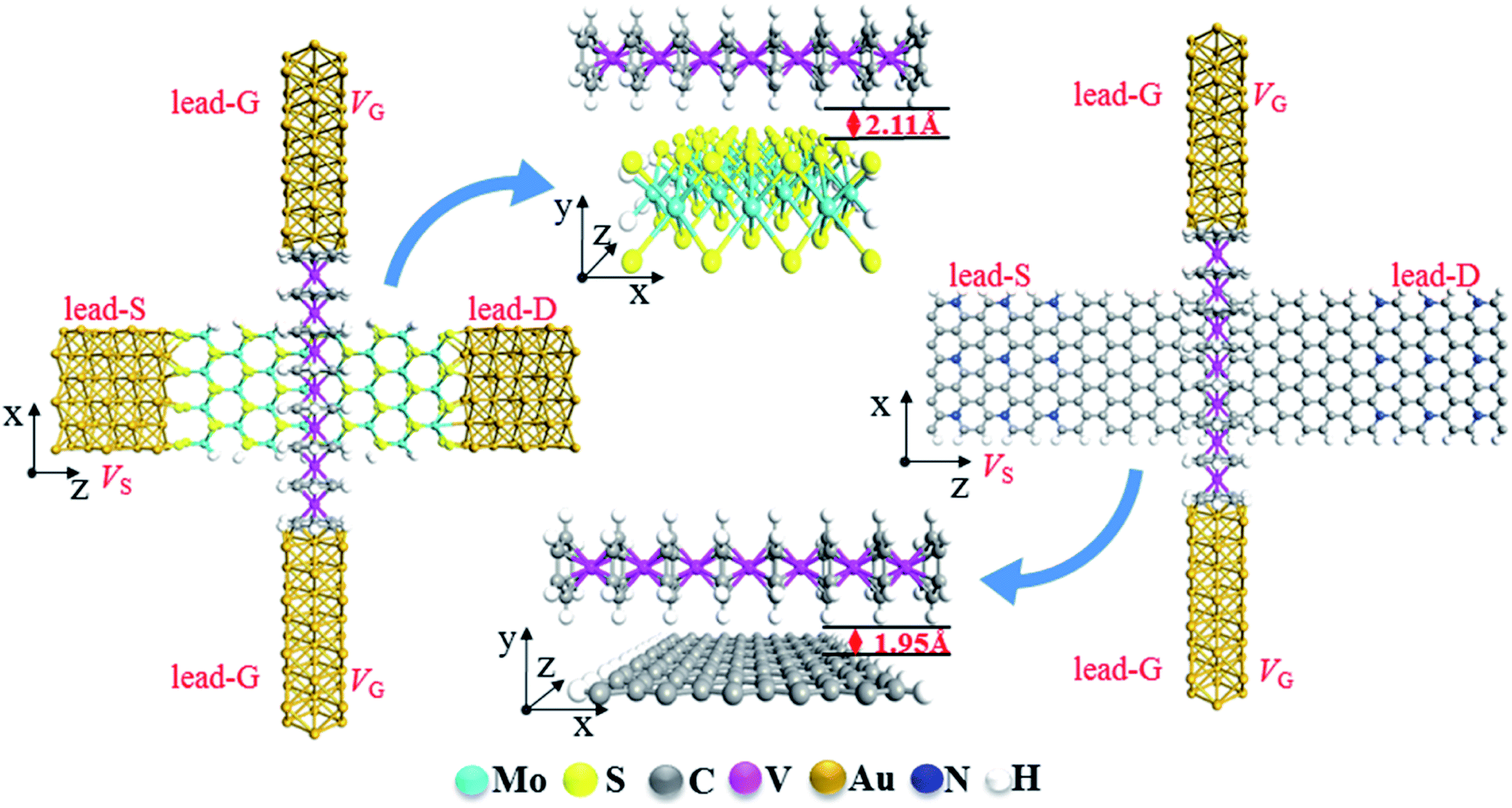 | ||
| Fig. 1 Schematic plots of MoS2/V7(Bz)8 and Graphene/V7(Bz)8 four-terminal devices. Where lead-S, lead-D, and lead-G represent the source, drain, and gate leads, respectively. VS and VG represent the bias voltage applied on lead-S and the gate voltage applied on lead-G, respectively. | ||
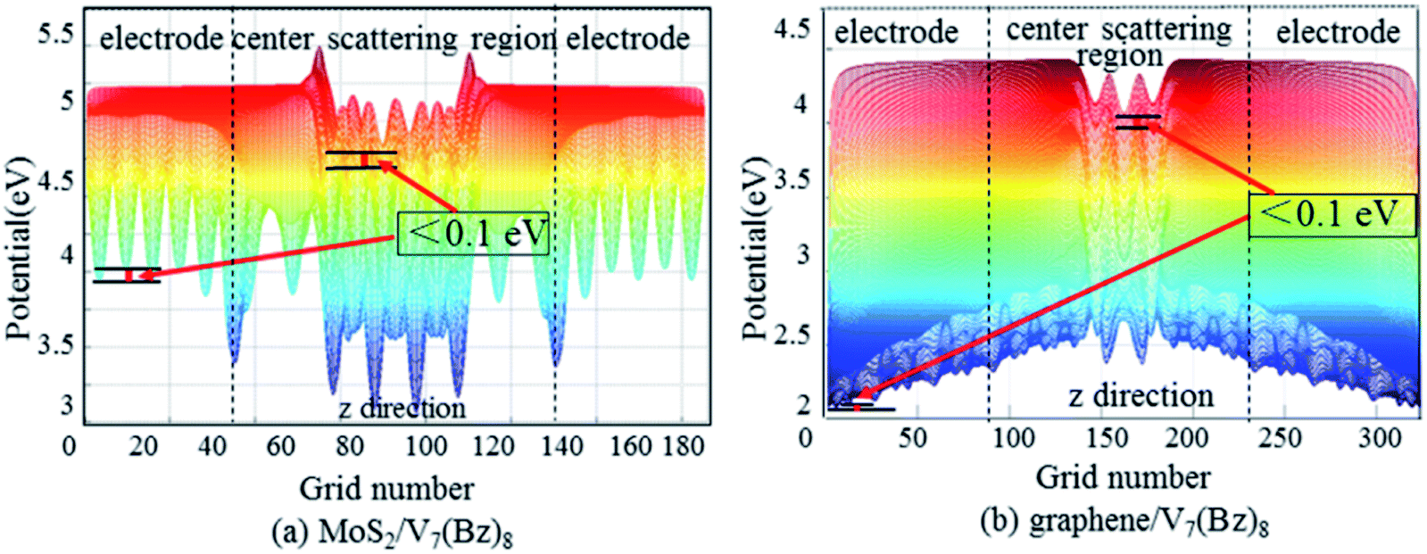 | ||
| Fig. 2 The calculated potential distribution of the buffers near the leads in the two four-terminal devices, (a) is that in MoS2/V7(Bz)8 device and (b) is that in graphene/V7(Bz)8 device. | ||
The DFT method with generalized gradient approximation (GGA) implemented in ATK package is employed to optimize the four-terminal structures. For both MoS2/V7(Bz)8 and graphene/V7(Bz)8 four-terminal devices, all the leads are frozen and the scatter regions are optimized. The self-consistent total energies are converged to 10−4 eV and the forces are converged to 0.05 eV Å−1. The optimized cartesian coordinates of all the models are given in Tables S1 and S2 in the ESI.† The optimized distance is 2.11 Å from MoS2 to V7(Bz)8 and 1.95 Å from graphene to V7(Bz)8, a typical vdW interaction. Then, the transport properties of the optimized devices are calculated using DFT with NEGF methodology within Nanodcal software package.55,56 The linear combination of atomic orbitals (LCAO) is employed to expand physical parameters. The standard nonlocal norm-conserving pseudopotentials is used to describe the atomic core, and the double-zeta polarized (DZP) basis set is for valence electronic orbitals.57,58 The exchange-correlation function is considered by the local density approximation (LDA).58,59 The k-point for the central region is meshed as 1 × 1 × 1 (x × y × z), and that is 1 × 1 × 100 for lead-S and lead-D, 100 × 1 × 1 for lead-G. It is worth noting that, in all calculations the spin of V atoms is considered by using LAD + U scheme, and the U–J is set as 3.0 eV.60 160 Rydberg cutoff energy is applied.
The spin-dependent current in leads for multi-terminal system can be obtained using the Landauer–Büttiker formula (1):57,61,62
 | (1) |
Considering the multi-terminals, the conductance between lead-α and lead-β can be evaluated by formula (2):
 | (2) |
3. Results and discussion
In this section, we mainly document on how the bias voltage (VS) and the gate voltage (VG) synergistically influence the transport properties of MoS2/V7(Bz)8 and graphene/V7(Bz)8 vdW junctions from the aspects of conductance, currents, LDOS, and transmission. The VS is set as 0.0, 0.2, 0.4 V, respectively. And at each certain VS, the VG ranges from 0.0 to 1.0 V by a step of 0.2 V.3.1 Conductivity
To convenient description, the channels between any two terminals are denoted as channel S–D, channel S–G, channel D–G, and channel G–G.Fig. 3 shows the calculated conductance of each channel of MoS2/V7(Bz)8 and graphene/V7(Bz)8 devices with the variation of VS and VG. For the sake of comparison, the scales of conductance in vertical-axle in Fig. 3 are the same for all the channels, and Fig. S1† with adapted vertical-axis scales is supplied as ESI.† The conductance is bigger than 0.8e2/h, in the range of 0.5–1.0e2/h, and smaller than 0.3e2/h for graphene channel S–D, V7(Bz)8 channel G–G, and MoS2 channel S-D, respectively. That is, the conductivity follows the sequence of MoS2 < V7(Bz)8 < graphene. Therefore, using V7(Bz)8 as gate may play different effects on tuning electron transporting through MoS2 and graphene. Since the V7(Bz)8 nanowire attaches to MoS2 and graphene via vdW interaction, the conductance of channels S–G and D–G are very small (<0.03e2/h). The potentials from gate and from source couple in different degrees in MoS2/V7(Bz)8 and graphene/V7(Bz)8 under various VS and VG. This integrates the change of resistance from source to drain, which makes the conductance goes up or down.
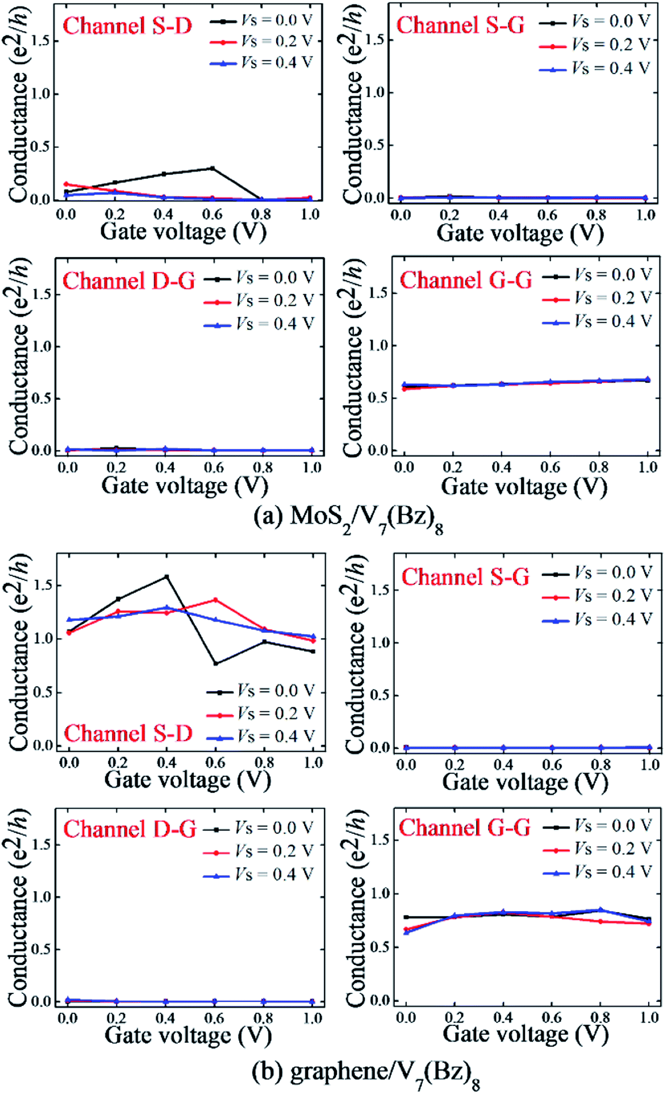 | ||
| Fig. 3 Conductance for channel S–D, channel S–G, channel D–G, and channel G–G as a function of VG at fixed values of VS = 0.0, 0.2, or 0.4 V of the four-terminal MoS2/V7(Bz)8 and graphene/V7(Bz)8 devices. (a and b) Are for the MoS2/V7(Bz)8 and graphene/V7(Bz)8 devices, respectively. | ||
3.2 Current
To further understand the transport property of the four-terminal devices, we calculated the total currents, IS, ID, and IG, passing through lead-S, lead-D, and lead-G, respectively. Currents from lead to center region are input and defined as positive values, while those from center region to lead are output and appointed as negative values.Fig. 4 displays the total currents through the leads with the variation of VS and VG applied on MoS2/V7(Bz)8 and graphene/V7(Bz)8 devices. Multi-channels in four-terminal devices could cause complicated transport properties aroused from the intricacy of channel couplings. Actually, the magnitude of each lead current comes from the synergistic action of all pathways. For example, though lead-S current is directly related to channels S–D and S–G, channels S–D and S–G are simultaneously influenced by channels D–G and G–G.
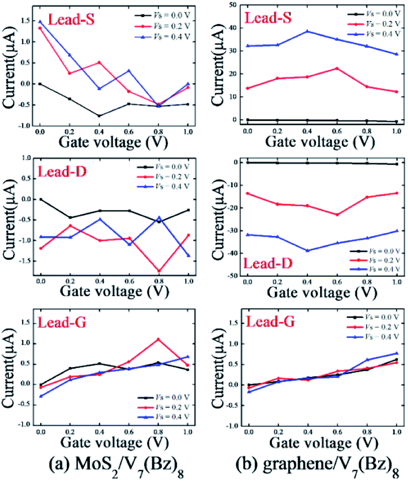 | ||
| Fig. 4 Total currents for lead-S, lead-D, and lead-G as a function of VG at fixed values of VS = 0.0, 0.2, or 0.4 V of the four-terminal devices, where (a) shows those in MoS2/V7(Bz)8 devices, and (b) is in graphene/V7(Bz)8. | ||
Now we consider the total currents, IS, ID, and IG of MoS2/V7(Bz)8 device (Fig. 4a). With free gate voltage, a small amount of current leaks off lead-G when applied VS = 0.2 and 0.4 V, while the lead-G current becomes input once VG imposed, which could exert considerable effect on the source-to-drain transporting. The lead-D currents are always output owing to its low voltage potential compared with other three leads. At VS = 0.0 V, lead-S and lead-D give output currents with the absolute values of IS < 1.0 μA and ID < 0.5 μA, which are induced by the applied gate voltages. Interestingly, regardless of any VS, the IS, ID, and IG curves present a pattern of up and down oscillation with the changing of VG, resulting in NDR peaks. Of course, the magnitude, the position, and the numbers of these NDR peaks are different for different leads at various VS and VG. In fact, conductivity, as a complicated phenomenon, relates to comprehensive factors such as scatter region structure, scatter region–lead interaction, couplings between channels, changes of resistance induced by voltages, etc. For example, the asymmetric character of MoS2 structure not only induces different resistance for different channels, but also induces different left and right MoS2–lead interactions. Therefore, at zero VS bias, the IS and ID curves give different shapes. All these comprehensive factors may also be responsible for the dissimilarity of the NDR behaviors of IS, ID, and IG. When nonzero VS is applied, as the VG increases, the input IS current decreases as a whole and could switches to output at certain VG, e.g., at VG = 0.6 V for VS = 0.2 V and at VG = 0.4 and 0.8 V for VS = 0.4 V. Therefore, the currents across lead-S are rather dependent on the interplay of VS and VG. At VS = 0.2 and 0.4 V, the absolute values of ID rise comparing with VS = 0.0 V. This is a reasonable result from the higher potential injected into the channel S–D. The magnitude of the output currents of lead-D tends to be balanced around 1.0 μA. All these properties are much desirable for designing functional devices with fascinating characteristics such as NDR behavior and input/output switching.
As to the graphene/V7(Bz)8 device, the total currents of IS, ID, and IG display a much different feature from MoS2/V7(Bz)8 as shown from Fig. 4b. Intuitively, the gate VG plays a small role on the carries transport via the graphene plane. This result can be deduced from two phenomena: one is that the magnitudes of IS and ID (10–40 μA) are much higher than IG (<1.0 μA) under applied VG; another is that the input values of IS are almost equal to the output data of ID at given VS and VG, indicating that the injected IS almost arrives to the lead-D completely. No evident NDR behavior is observed for graphene/V7(Bz)8. In addition, unlike in MoS2/V7(Bz)8 which there exists input/output switching of lead-S, the current of lead-S in graphene/V7(Bz)8 is always input within the considered gate bias. The reason for these different phenomena between MoS2/V7(Bz)8 and graphene/V7(Bz)8 lies in the fact that graphene has higher conductivity than MoS2.
To investigate how the spin-polarized character of V7(Bz)8 influence the transport property of MoS2/V7(Bz)8 and graphene/V7(Bz)8, we computed the spin-up currents, IS↑, ID↑, and IG↑ as well as the spin-down currents, IS↓, ID↓, and IG↓, for lead-S, lead-D, and lead-G, respectively. The results are plotted in Fig. 5 and 6 as a function of VG at a given VS.
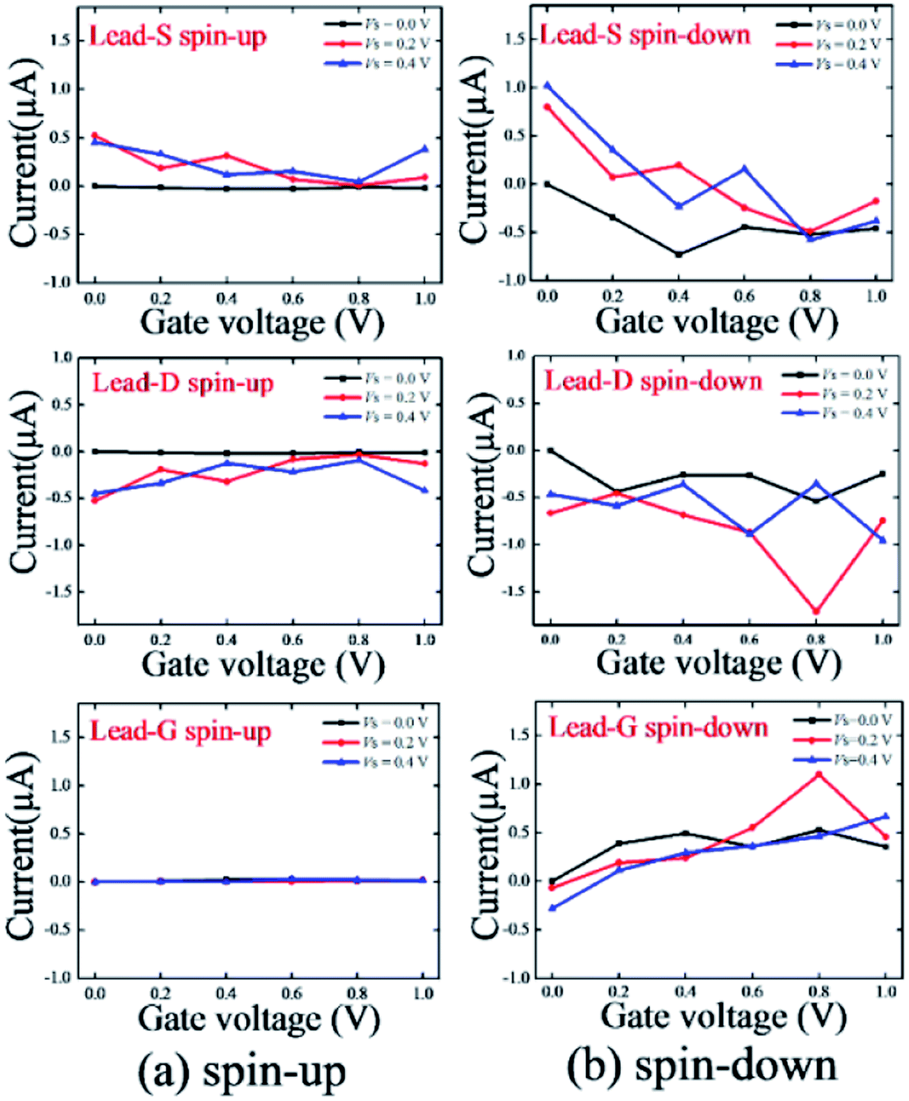 | ||
| Fig. 5 Spin currents for lead-S, lead-D, and lead-G as a function of VG at fixed values of VS = 0.0, 0.2, or 0.4 V of the four-terminal MoS2/V7(Bz)8 device. (a) Depicts the spin-up states of MoS2/V7(Bz)8, and (b) depicts those for spin-down state, respectively. | ||
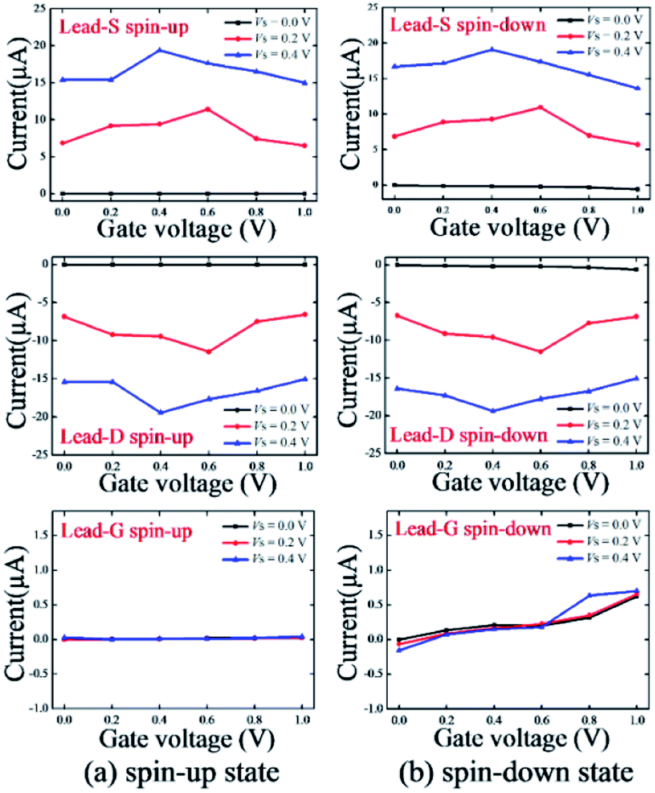 | ||
| Fig. 6 Spin currents for lead-S, lead-D, and lead-G as a function of VG at fixed values of VS = 0.0, 0.2, or 0.4 V of the four-terminal graphene/V7(Bz)8 device. (a) Depicts the spin-up states, and (b) depicts those for spin-down state, respectively. | ||
As expected, for V7(Bz)8 in both two devices, the IG↑ remains nearly zero, while the IG↓ possesses the same magnitude to the total IG. This thoroughly inherits the intrinsic spin-polarized feature of pure V7(Bz)8.60,63 Quite significantly, the spin polarized feature of V7(Bz)8 induces different polarized transport property from MoS2/V7(Bz)8 to graphene/V7(Bz)8. In the case of MoS2/V7(Bz)8, spin-up and spin-down channels of lead-S and lead-G are split by the polarization property of V7(Bz)8. At VS = 0.0 V, the spin-up paths of both lead-S and lead-D of MoS2/V7(Bz)8 are closed with almost zero current, and the total currents IS and ID entirely come from the spin-down IS↓ and ID↓. This is mainly due to the fact that the spin-up channel of V7(Bz)8 is almost closed and hence cannot cause perturbation on the spin-up pathway of MoS2. On the contrary, the spin-down state of V7(Bz)8 dominates electron transporting, enabling strong coupling with the spin-down channel of MoS2. Under nonzero VS, the currents through lead-S and lead-D in MoS2/V7(Bz)8 are polarized by a large extent. For the spin-up state, the currents of IS↑ are all input and those of ID↑ are all output. Both IS↑ and ID↑ curves of MoS2/V7(Bz)8 change smoothly in a small scale of 0.0–0.5 μA along the variation of VG. In striking contrast, the spin-down currents of IS↓ and ID↓ fluctuate significantly with the changing of VG, with a large range of from 1.0 to −0.5 μA for IS↓ and from 0.0 to −1.7 μA for ID↓. Observed carefully, one can find that the changing trends of IS↓ and ID↓ curves are roughly analogous to those of the total IS and ID. The NDR behavior and the input/output switch character of MoS2/V7(Bz)8 are mainly dominated by the spin-down state. Now turn to graphene/V7(Bz)8, quite different from MoS2/V7(Bz)8, no matter what VS and VG applied, the spin-up currents are almost equivalent to spin-down values for both lead-S and lead-D. Though the polarized characteristic of V7(Bz)8 is preserved in graphene/V7(Bz)8, its conductivity is too much weaker than graphene that can not exert valid influence on channel S–D.
3.3 Local density of states
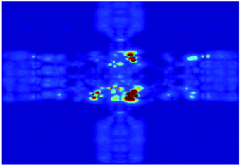
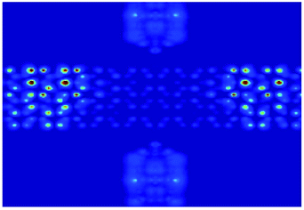
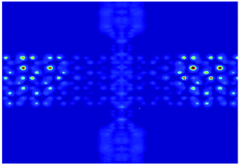
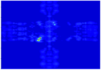
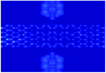
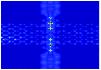
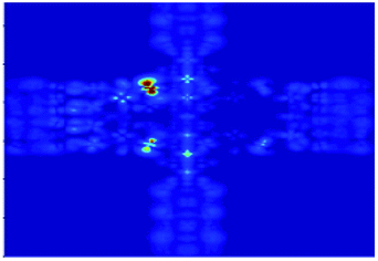
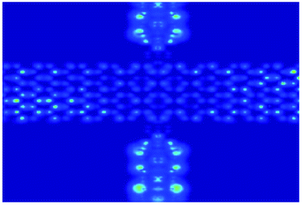
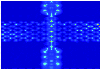
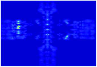
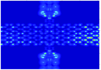
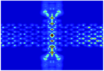
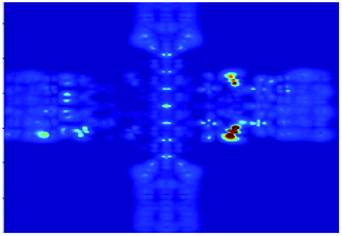
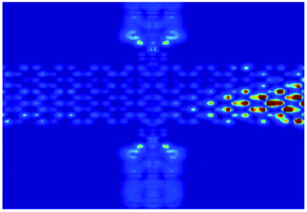
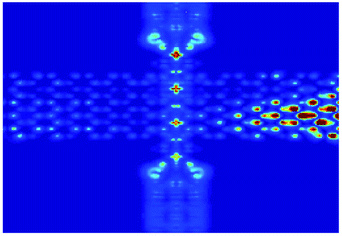
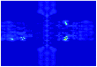
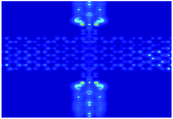
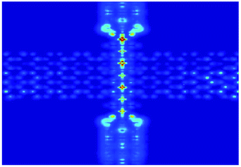
Table 1 displays the computed local density of states (LDOS) results of two devices under VS = 0.2 V, where the even LDOS distribution suggests an effective transport channel. The scenario of the polarized transport behavior of MoS2/V7(Bz)8 leads becomes more obvious by analyzing the LDOS distributions. As representative example, it is clear that the LDOS of the spin-down state of V7(Bz)8 delocalizes stronger than the spin-up state, which could bring about coupling with the spin-down state of MoS2, and consequently, lead to the spin-polarized splitting of MoS2/V7(Bz)8. The electronic potential on the whole system changes along with the relative magnitude of VS and VG, as can be reflected from the LDOS distributions. Clearly, charge carries in the spin-up state of either channel S–D or channel G–G are blocked more seriously than the spin-down state. As for the graphene/V7(Bz)8 device, the spin-down passage of V7(Bz)8 is open with uniform LDOS distribution while the spin-up path is closed with almost no LDOS. Despite of the maintained polarized character of V7(Bz)8, spin-up and spin-down channels along graphene has nearly identical LDOS spreading. This again demonstrates the unpolarized character of lead-S and lead-D currents.| VG (V) | LDOS at VS = 0.2 V | |||
|---|---|---|---|---|
| MoS2/V7(Bz)8 device | Graphene/V7(Bz)8 device | |||
| Spin-up | Spin-down | Spin-up | Spin-down | |
| 0.0 | 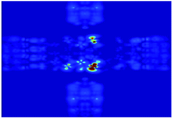 |
 |
 |
 |
| 0.2 | 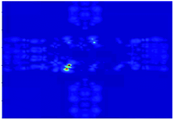 |
 |
 |
 |
| 0.4 | 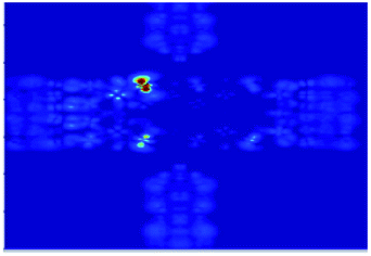 |
 |
 |
 |
| 0.6 | 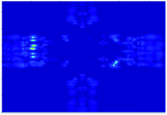 |
 |
 |
 |
| 0.8 | 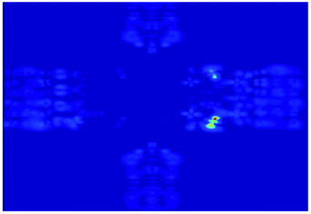 |
 |
 |
 |
| 1.0 | 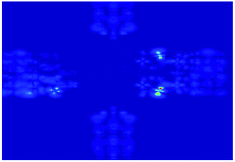 |
 |
 |
 |
3.4 Transmission coefficients and spectra
To further shed light on how the gate bias tune the transport property of MoS2/V7(Bz)8 and graphene/V7(Bz)8 devices, we computed spin polarized transmission coefficients (TC) of each channel at the case of VS = 0.0 V and VG from 0.0 to 1.0 V, and the results are shown in Fig. 7.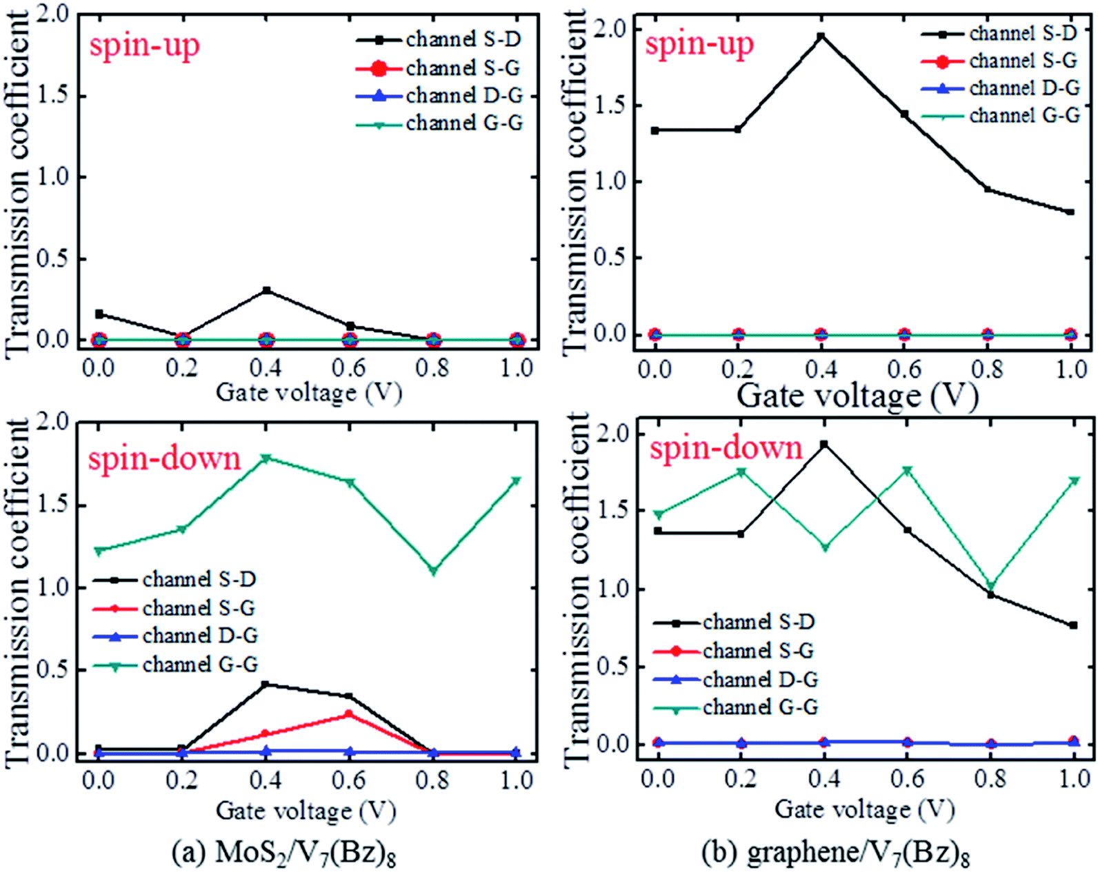 | ||
| Fig. 7 Transmission coefficient of all channels in two devices with variational VG from 0.0 to 1.0 V at VS = 0 V. (a) Shows spin-up and spin-down state in MoS2/V7(Bz)8 device, and (b) is that for graphene/V7(Bz)8 device. | ||
Evidently, in both MoS2/V7(Bz)8 and graphene/V7(Bz)8 devices, spin-down channel G–G composed of V7(Bz)8 has much higher TC than other channels, again demonstrating the preserved striking half-metallic character of V7(Bz)8. One can find that, in MoS2/V7(Bz)8, the main channel S–D consisting of MoS2 can not be largely influenced by the spin polarized character of the gate V7(Bz)8, as can be clearly seen from the comparable spin-up and spin-down TC. However, the spin polarized V7(Bz)8 directly consists of channels S–G and D–G, and thereby, it could induce spin split of channels S–G and D–G and generate larger spin-down TC than spin-up TC. Therefore, the spin polarized transport character of MoS2/V7(Bz)8 mainly derives from the perturbation of the spin-down state of V7(Bz)8 upon the channels S–G and D–G. Regarding graphene/V7(Bz)8, charge carriers can easily flow from lead-S to lead-D since channel S–D has large TC, while other channels are almost closed with nearly zero TC except the spin-down channel G–G. In addition, spin-up and spin-down states of channel S–D display the same TC curves, illustrating the ignoring polarization influence of V7(Bz)8 on graphene.
Furtherly, we calculated the transmission spectra (TS) of the main channel S–D for MoS2/V7(Bz)8 and graphene/V7(Bz)8 devices at each VS and VG, as plotted in Fig. 8. In the case of MoS2/V7(Bz)8, at VS = 0.0 V and VG = 0.0 V, TS peak located above the Ef mainly arises from the native MoS2. When adding VG merely, an extra peak appears near the Ef owing to the gate carries injection into the channel S–D of MoS2/V7(Bz)8. Once adding VS together with VG, only one peak exists below the Ef due to the suppression effect of the incoming VG potential upon the VS. Furthermore, with the increasing of VG, such suppression effect in MoS2/V7(Bz)8 becomes more significant, as the TS peak moves farer away from the Ef. In contrast, regardless of VS and VG, lots of TS peaks of channel S–D appear around the Ef of graphene/V7(Bz)8, again indicating the high conductivity of graphene.
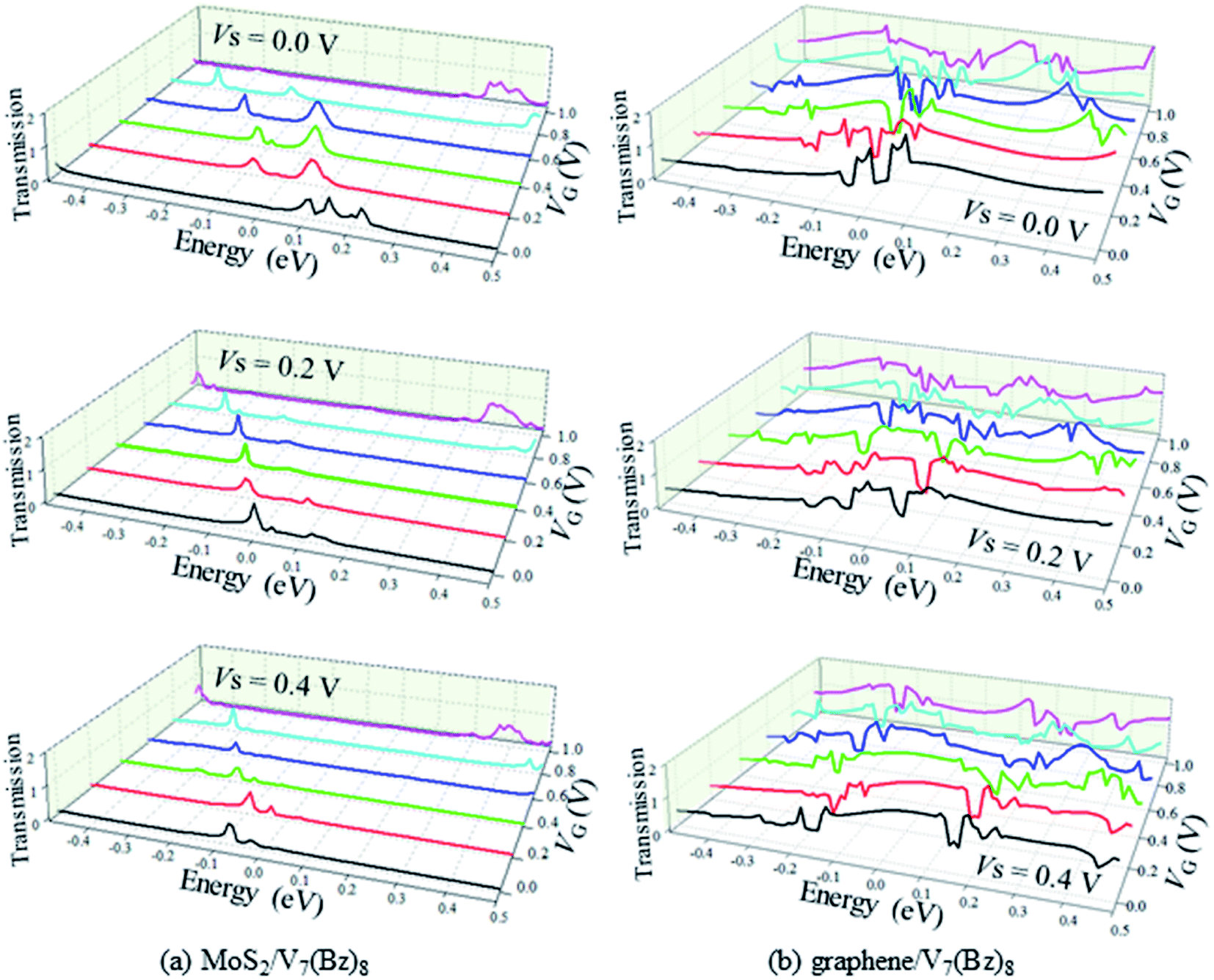 | ||
| Fig. 8 Transmission spectra of channel S–D in MoS2/V7(Bz)8 and graphene/V7(Bz)8 device with variational VG from 0.0 to 1.0 V at a certain VS, where (a) depicts the case in MoS2/V7(Bz)8, and (b) is that for graphene/V7(Bz)8, respectively. | ||
4. Conclusion
The MoS2/V7(Bz)8 and graphene/V7(Bz)8 vdW junctions are designed and the transport properties of their four-terminal devices are comparatively investigated based on the DFT and NEGF techniques. The MoS2 and graphene nanoribbons act as the source-to-drain channel and the spin-polarized V7(Bz)8 nanowire serves as the gate channel. The transport characteristic is explored by investigating the conductance, currents, LDOS, and transmission spectra. Gate voltages applied on V7(Bz)8 exert different influences of electron transporting on MoS2/V7(Bz)8 and graphene/V7(Bz)8. The interplay of source and gate bias potentials generates a pronounced influence on the transport property of MoS2/V7(Bz)8. Evident NDR behavior, input/output current switches, as well as spin-polarized currents are found for MoS2/V7(Bz)8. In contrast, the gate bias plays insignificant effect on the transporting along graphene. These results are promising in designing multi-terminal nanoelectronic devices.Conflicts of interest
There are no conflicts of interest to declare.Acknowledgements
This work was supported by the National Natural Science Foundation of China (Grant No. 51973046). And more, We gratefully acknowledge HZWTECH for providing computation facilities.References
- Q. Lv, F. Yan, N. Mori, W. Zhu, C. Hu, Z. R. Kudrynskyi, Z. D. Kovalyuk, A. Patane and K. Wang, Interlayer band-to-band tunneling and negative differential resistance in van der Waals BP/InSe field-effect transistors, Adv. Funct. Mater., 2020, 30, 1910713 CrossRef CAS.
- B. Jiang, X. Zou, J. Su, J. Liang, J. Wang, H. Liu, L. Feng, C. Jiang, F. Wang, J. He and L. Liao, Impact of thickness on contact issues for pinning effect in black phosphorus field-effect transistors, Adv. Funct. Mater., 2018, 28, 1801398 CrossRef.
- W. Ahmad, Y. N. Gong, G. Abbas, K. Khan, M. Khan, G. Ali, A. Shuja, A. K. Tareen, Q. Khan and D. L. Li, Evolution of low-dimensional material-based field-effect transistors, Nanoscale, 2021, 13, 5162 RSC.
- J. L. Du, H. H. Yu, B. S. Liu, M. Y. Hong, Q. L. Liao, Z. Zhang and Y. Zhang, Strain engineering in 2d material-based flexible optoelectronics, Small Methods, 2020, 5, 2000919 CrossRef PubMed.
- Z. X. Li, D. Y. Li, H. Y. Wang, P. Chen, L. J. Pi, X. Zhou and T. Y. Zhai, Intercalation strategy in 2D materials for electronics and optoelectronics, Small Methods, 2021, 5, 2100567 CrossRef CAS PubMed.
- Y. K. Liao, Z. F. Zhang, Z. B. Gao, Q. K. Qian and M. Y. Hua, Tunable properties of novel Ga2O3 monolayer for electronic and optoelectronic applications, ACS Appl. Mater. Interfaces, 2020, 12, 30659–30669 CrossRef CAS PubMed.
- E. Singh, P. Singh, K. S. Kim, G. Y. Yeom and H. S Nalwa, Flexible molybdenum disulfide (MoS2) atomic layers for wearable electronics and optoelectronics, ACS Appl. Mater. Interfaces, 2019, 11, 11061–11105 CrossRef CAS PubMed.
- Y. P. Liu, C. Zeng, J. H. Zhong, J. N. Ding, Z. M. Wang and Z. W. Liu, Spintronics in two-dimensional materials, Nano-Micro Lett., 2020, 12, 93 CrossRef CAS PubMed.
- C. K. Safeer, J. Ingla-Aynés, F. Herling, J. H. Garcia, M. Vila, N. Ontoso, M. R. Calvo, S. Roche, L. E. Hueso and F. Casanova, Room temperature spin Hall effect in graphene/MoS2 van der Waals heterostructures, Nano Lett., 2019, 19, 1074–1082 CrossRef CAS PubMed.
- A. Avsar, H. Ochoa, F. Guinea, B. Ozyilmaz, B. J. Van Wees and I. J. Vera-Marun, Colloquium: spintronics in graphene and other two-dimensional materials, Rev. Mod. Phys., 2020, 92, 021003 CrossRef CAS.
- A. P. Johnson, C. Sabu, N. K. Swamy, A. Anto, H. V. Gangadharappa and K. Pramod, Graphene nanoribbon: an emerging and efficient flat molecular platform for advanced biosensing, Biosens. Bioelectron., 2021, 184, 113245 CrossRef CAS PubMed.
- Y. J. Gao, J. L. Chen, G. R. Chen, C. H. Fan and X. G. Liu, Recent progress in the transfer of graphene films and nanostructures, Small Methods, 2021, 5, 2100771 CrossRef CAS PubMed.
- S. Achra, T. Akimoto, J. F. de Marneffe, S. Sergeant, X. Y. Wu, T. Nuytten, S. Brems, I. Asselberghs, Z. Tokei and K. Ueno, Enhancing interface doping in graphene-metal hybrid devices using H-2 plasma clean, Appl. Surf. Sci., 2021, 538, 148046 CrossRef CAS.
- K. M. Wyss, D. X. Luong and J. M. Tour, Large-scale syntheses of 2d materials: flash joule heating and other methods, Adv. Mater., 2022, 34, 2106970 CrossRef CAS PubMed.
- I. Alcón, G. Calogero, N. Papior and M. Brandbyge, Electrochemical control of charge current flow in nanoporous graphene, Adv. Funct. Mater., 2021, 31, 2104031 CrossRef.
- T. Chen, W. C. Ding, H. L. Li and G. H. Zhou, Length-independent multifunctional device based on penta-tetra-pentagonal molecule: a first-principles study, J. Mater. Chem. C, 2021, 9, 3652 RSC.
- Q. Sun, X. L. Yao, O. Groning, K. Eimre, C. A. Pignedoli, K. Muellen, A. Narita, R. Fasel and P. Ruffieux, Coupled spin states in armchair graphene nanoribbons with asymmetric zigzag edge extensions, Nano Lett., 2020, 20, 6429–6436 CrossRef CAS.
- P. L. Zhao, J. Yu, H. Zhong, M. Rosner, M. I. Katsnelson and S. J. Yuan, Electronic and optical properties of transition metal dichalcogenides under symmetric and asymmetric field-effect doping, New J. Phys., 2020, 22, 083072 CrossRef CAS.
- S. Y. Seo, D. H. Yang, G. Moon, O. F. N. Okello, M. K. Park, S. H. Lee, S. Y. Choi and M. H. Jo, Identification of point defects in atomically thin transition-metal dichalcogenide semiconductors as active dopants, Nano Lett., 2021, 21, 3341–3354 CrossRef CAS PubMed.
- T. K. Rao, H. D. Wang, Y. J. Zeng, Z. N. Guo, H. Zhang and W. G. Liao, Phase transitions and water splitting applications of 2D transition metal dichalcogenides and metal phosphorous trichalcogenides, Adv. Sci., 2021, 8, 2002284 CrossRef CAS PubMed.
- S. S. Li, H. Wang, J. Wang, H. J. Chen and L. Shao, Control of light-valley interactions in 2D transition metal dichalcogenides with nanophotonic structures, Nanoscale, 2021, 13, 6357 RSC.
- Y. C. Lin, R. Torsi, D. B. Geohegan, J. A. Robinson and K. Xiao, Controllable thin-film approaches for doping and alloying transition metal dichalcogenides monolayers, Adv. Sci., 2021, 8, 2004249 CrossRef CAS PubMed.
- S. Wang, M. S. Ukhtary and R. Saito, Strain effect on circularly polarized electroluminescence in transition metal dichalcogenides, Phys. Rev. Res., 2020, 2, 033340 CrossRef CAS.
- Y. F. Zhang, J. B. Pan and S. X. Du, Geometric, electronic, and optical properties of MoS2/WSSe van der Waals heterojunctions: a first-principles study, Nanotechnology, 2021, 32, 355705 CrossRef CAS PubMed.
- X. T. Yu, X. Wang, F. F. Zhou, J. L. Qu and J. Song, 2D van der Waals heterojunction nanophotonic devices: from fabrication to performance, Adv. Funct. Mater., 2021, 31, 2104260 CrossRef CAS.
- S. Q. Hu, J. P. Xu, Q. H. Zhao, X. G. Luo, X. T. Zhang, T. Wang, W. Q. Jie, Y. C. Cheng, R. Frisenda, A. Castellanos-Gomez and X. T. Gan, Gate-switchable photovoltaic effect in BP/MoTe2 van der Waals heterojunctions for self-driven logic optoelectronics, Adv. Opt. Mater., 2020, 9, 2001802 CrossRef.
- H. D. Wang, S. Gao, F. Zhang, F. X. Meng, Z. N. Guo, R. Cao, Y. H. Zeng, J. L. Zhao, S. Chen, H. G. Hu, Y. J. Zeng, S. J. Kim, D. Y. Fan, H. Zhang and P. N. Prasad, Repression of Interlayer recombination by graphene generates a sensitive nanostructured 2d vdW heterostructure based photodetector, Adv. Sci., 2021, 8, 2100503 CrossRef CAS PubMed.
- R. C. Luo, W. W. Xu, Y. Z. Zhang, Z. Q. Wang, X. D. Wang, Y. Ga, P. Liu and M. W. Chen, Van der Waals interfacial reconstruction in monolayer transition-metal dichalcogenides and gold heterojunctions, Nat. Commun., 2020, 11, 1011 CrossRef CAS PubMed.
- L. Yuan, B. Y. Zheng, J. Kunstmann, T. Brumme, A. B. Kuc, C. Ma, S. B. Deng, D. Blach, A. Pan and L. B. Huang, Twist-angle-dependent interlayer exciton diffusion in WS2-WSe2 heterobilayers, Nat. Mater., 2020, 19, 617–623 CrossRef CAS PubMed.
- X. D. Guo, R. N. Liu, D. B. Hu, H. Hu, Z. Wei, R. Wang, Y. Y. Dai, Y. Cheng, K. Chen, K. H. Liu, G. Y. Zhang, X. Zhu, Z. P. Sun, X. X. Yang and Q. Dai, Efficient all-optical plasmonic modulators with atomically thin van der Waals heterostructures, Adv. Mater., 2020, 32, 1907105 CrossRef CAS PubMed.
- C. L. Tang, Z. W. Zhang, S. Lai, Q. H. Tan and W. B. Gao, Magnetic proximity effect in graphene/CrBr3 van der Waals heterostructures, Adv. Mater., 2020, 32, 1908498 CrossRef CAS PubMed.
- K. S. Kamal, W. C. Lu, J. Bernholc and V. Meunier, Electron transport in multiterminal molecular devices: A density functional theory study, Phys. Rev. B: Condens. Matter Mater. Phys., 2010, 81, 125420 CrossRef.
- M. W. Iqbala, K. Shahzada, H. Ateeqa, I. Aslamb, S. Aftabc, S. Azama, M. A. Kamrand and M. F. Khan, An effectual enhancement to the electrical conductivity of graphene FET by silver nanoparticles, Diamond Relat. Mater., 2020, 106, 107833 CrossRef.
- Y. B. Hu, J. S. Yoo, H. T. Ji, A. Goodman and X. M. Wu, Probe measurements of electric field and electron density fluctuations at megahertz frequencies using in-shaft miniature circuits, Rev. Sci. Instrum., 2021, 92, 033534 CrossRef CAS PubMed.
- D. V. Gruznev, L. V. Bondarenko, A. Y. Tupchaya, V. G. Kotlyar, O. A. Utas, A. N. Mihalyuk, N. V. Denisov, A. V. Matetskiy, A. V. Zotov and A. A. Saranin, Atomic, electronic and transport properties of In-Au 2D compound on Si(100), J. Phys.: Condens. Matter, 2019, 32, 135003 CrossRef PubMed.
- N. Papadopoulos, E. Flores, K. Watanabe, T. Taniguchi, J. R. Ares, C. Sanchez, I. J. Ferrer, A. Castellanos-Gomez, G. A. Steele and H. S. J. van der Zant, Multi-terminal electronic transport in boron nitride encapsulated TiS3 nanosheets, 2D Mater., 2019, 7, 015009 CrossRef.
- N. V. Denisov, A. V. Matetskiy, A. N. Mihalyuk, S. V. Eremeev, S. Hasegawa, A. V. Zotov and A. A. Saranin, Superconductor-insulator transition in an anisotropic two-dimensional electron gas assisted by one-dimensional Friedel oscillations: (Tl, Au)/Si(100)-c(2 × 2), Phys. Rev. B: Condens. Matter Mater. Phys., 2019, 100, 155412 CrossRef CAS.
- J. Q. Zhou, J. F. Qiao, C. G. Duan, A. Bournel, K. L. Wang and W. S. Zhao, Large tunneling magnetoresistance in VSe2/MoS2 magnetic tunnel junction, ACS Appl. Mater. Interfaces, 2019, 11, 17647–17653 CrossRef CAS PubMed.
- H. Y. Zhou, Y. G. Zhang and W. S. Zhao, Tunable tunneling magnetoresistance in van der Waals magnetic tunnel junctions with 1T-CrTe2 electrodes, ACS Appl. Mater. Interfaces, 2021, 13, 1214–1221 CrossRef CAS PubMed.
- Y. L. Guo, Y. H. Zhang, Z. B. Zhou, X. W. Zhang, B. Wang, S. J. Yuan, S. Dong and J. L. Wang, Spin-constrained optoelectronic functionality in two-dimensional ferromagnetic semiconductor heterojunctions, Mater. Horiz., 2021, 8, 1323 RSC.
- S. K. Behera and P. Deb, Spin-transfer-torque mediated quantum magnetotransport in MoS2/phosphorene vdW heterostructure based MTJs, Phys. Chem. Chem. Phys., 2020, 22, 19139 RSC.
- K. Miyajima, A. Nakajima, S. Yabushita, M. B. Knickelbein and K. Kaya, Ferromagnetism in one-dimensional vanadium-benzene sandwich clusters, J. Am. Chem. Soc., 2004, 126, 13202–13203 CrossRef CAS PubMed.
- M. Mitsui, S. Nagaoka, T. Matsumoto and A. Nakajima, Soft-landing isolation of Vanadium−Benzene sandwich clusters on a room-temperature substrate using-alkanethiolate self-assembled monolayer matrixes, J. Phys. Chem. B, 2006, 110, 2968–2971 CrossRef CAS.
- J. Wang, H. P. Acioli and J. Jellinek, Structure and magnetism of VnBzn+1 sandwich clusters, J. Am. Chem. Soc., 2005, 127, 2812–2813 CrossRef CAS PubMed.
- S. Nagao, A. Kato and A. Nakajima, Multiple-decker sandwich poly-ferrocene clusters, J. Am. Chem. Soc., 2000, 122, 4221–4222 CrossRef CAS.
- X. Y. Liang, G. L. Zhang, P. Sun, Y. Shang, Z. D. Yang and X. C. Zeng, The electronic and transport properties of (VBz)n@CNT and (VBz)n@BNNT nanocables, J. Mater. Chem. C, 2015, 3, 4039 RSC.
- S. B. Desai, S. R. Madhvapathy, A. B. Sachid, J. P. Llinas, Q. Wang, G. H. Ahn, G. Pitner, M. J. Kim, J. Bokor, C. Hu, H. S. P. Wong and A. Javey, MoS2 transistors with 1-nanometer gate lengths, Science, 2016, 354, 99–102 CrossRef CAS PubMed.
- A. Antušek, M. Blaško, M. Urban, P. Noga, D. Kisić, M. Nenadović, D. Lončarevićd and Z. Rakočević, Density functional theory modeling of C–Au chemical bond formation in gold implanted polyethylene, Phys. Chem. Chem. Phys., 2017, 19, 28891–28906 RSC.
- S. S. Li, H. Yu, G. L. Zhang and Y. Y. Hu, Four probe electron transport characteristics porphyrin phenylacetylene molecule devices, New J. Chem., 2020, 45, 2520–2528 RSC.
- D. Jariwala, V. K. Sangwan, D. J. Late, J. E. Johns, V. P. Dravid, T. J. Marks, L. J. Lauhon and M. C. Hersam, Band-like transport in high mobility unencapsulated single-layer MoS2 transistors, Appl. Phys. Lett., 2013, 102, 173107 CrossRef.
- H. Yu, Y. Shang, L. Pei, G. L. Zhang and H. Yan, Spin-polarized gate tuned transport property of a four-terminal MoS2 device: a theoretical study, J. Mater. Sci., 2021, 56, 11847–11865 CrossRef CAS.
- A. Nourbakhsh, A. Zubair, M. S. Dresselhaus and T. Palacios, Transport properties of a MoS2/WSe2 heterojunction transistor and its potential for application, Nano Lett., 2016, 16, 1359–1366 CrossRef CAS PubMed.
- L. T. Qu, Y. Liu, J. B. Baek and L. M. Dai, Nitrogen-doped graphene as efficient metal-free electrocatalyst for oxygen reduction in fuel cells, ACS Nano, 2010, 4, 1321–1326 CrossRef CAS.
- Y. X. Wang, Y. J. Jiang, S. N. Gao, H. Yu, G. L. Zhang and F. M. Zhang, Tuning magnetism and transport property of planar and wrinkled FePP@GNR hybrid materials, AIP Adv., 2020, 10, 045112 CrossRef CAS.
- J. Taylor, H. Guo and J. Wang, Ab initio modeling of quantum transport properties of molecular electronic devices, Phys. Rev. B: Condens. Matter Mater. Phys., 2001, 63, 245407 CrossRef.
- B. Wang, J. Wang and H. Guo, Ab initio calculation of transverse spin current in graphene nanostructures, Phys. Rev. B, 2009, 79, 165417 CrossRef.
- H. C. Lü, Y. Zhang, X. J. Liu, Y. Wang, Q. Zhang and H. T. Yin, Theoretical limit of how small we can make MoS2 transistor channels, J. Phys. D: Appl. Phys., 2022, 55, 105304 CrossRef.
- J. Junquera, Ó. Paz, D. Sánchez-Portal and E. Artacho, Numerical atomic orbitals for linear-scaling calculations, Phys. Rev. B, 2001, 64, 235111 CrossRef.
- X. Liu, Y. Z. Tan, Z. Y. Ma and Y. Pei, First-principles study of structural, electronic, and magnetic properties of one-dimensional transition metals incorporated vinylnaphthalene molecular wires on hydrogen-terminated silicon surface, J. Phys. Chem. C, 2016, 120, 27980–27988 CrossRef CAS.
- I. Solovyev, N. Hamada and K. Terakura, t2g versus all 3d localization in LaMO3 perovskites (M = Ti–Cu): First-principles study, Phys. Rev. B: Condens. Matter Mater. Phys., 1996, 53, 7158–7170 CrossRef CAS PubMed.
- M. Büttiker, Y. Imry, R. Landauer and S. Pinhas, Generalized many-channel conductance formula with application to small rings, Phys. Rev. B: Condens. Matter Mater. Phys., 1985, 31, 6207–6215 CrossRef PubMed.
- H. Wang, J. Zhou, X. J. Liu, C. B. Yao, H. Li, L. Niu, Y. Wang and H. T. Yin, Spin transport through a junction entirely consisting of molecules from first principles, Appl. Phys. Lett., 2017, 111, 172408 CrossRef.
- T. Gan, G. L. Zhang, Y. Shang, X. H. Su, Z. D. Yang and X. J. Sun, Electronic and transport properties of the (VBz)n@MoS2NT nanocable, Phys. Chem. Chem. Phys., 2016, 18, 4385–4393 RSC.
Footnote |
| † Electronic supplementary information (ESI) available. See https://doi.org/10.1039/d2ra02196j |
| This journal is © The Royal Society of Chemistry 2022 |