
 Open Access Article
 This Open Access Article is licensed under a Creative Commons Attribution-Non Commercial 3.0 Unported Licence
High-Q refractive index sensors based on all-dielectric metasurfaces
Pinghui Wu *,
Shuangcao Qu,
Xintao Zeng,
Ning Su,
Musheng Chen and
Yanzhong Yu
*,
Shuangcao Qu,
Xintao Zeng,
Ning Su,
Musheng Chen and
Yanzhong Yu
Research Center for Photonic Technology, Fujian Provincial Key Laboratory for Advanced Micro-nano Photonics Technology and Devices & Key Laboratory of Information Functional Material for Fujian Higher Education, Quanzhou Normal University, Quanzhou 362000, China. E-mail: phwu@zju.edu.cn
First published on 2nd August 2022
Abstract
Possessing fantastic abilities to freely manipulate electromagnetic waves on an ultrathin platform, metasurfaces have aroused intense interest in the academic circle. In this work, we present a high-sensitivity refractive index sensor excited by the guided mode of a two-dimensional periodic TiO2 dielectric grating structure. Numerical simulation results show that the optimized nanosensor can excite guided-mode resonance with an ultra-narrow linewidth of 0.19 nm. When the thickness of the biological layer is 20 nm, the sensitivity, Q factor, and FOM values of the nanosensor can reach 82.29 nm RIU−1, 3207.9, and 433.1, respectively. In addition, the device shows insensitivity to polarization and good tolerance to the angle of incident light. This demonstrates that the utilization of low-loss all-dielectric metasurfaces is an effective way to achieve ultra-sensitive biosensor detection.
1. Introduction
Metamaterials are periodic or aperiodic arrays of sub-wavelength artificial three-dimensional (3D) material units with extraordinary electromagnetic properties.1–5 Due to the advancement of micro/nano processing technology and the unique optics of sub-wavelength structure characteristics, metamaterials are being widely used in ultra-sensitive biochemical sensors, slow optical devices, photocatalysis and optical modulation devices.6–10 However, the development and application of metamaterials are greatly restricted by the disadvantages of their complex 3D systems, large device size, and high loss of metal structures, especially in the high-frequency (terahertz, infrared and optical) band,11,12 which are very difficult to process. With the emergence of metasurfaces in 2011, they have steadily grabbed the attention of researchers.13 Metasurfaces are low-loss planar structures, which can be regarded as an extension of the two-dimensional (2D) form of metamaterials.14,15 Compared with metamaterials, metasurfaces overcome the bottlenecks of the difficulty in processing and the high loss of metamaterials, providing convenience for the integration and miniaturization of nano-optical devices. Traditional refractive index sensors are mainly composed of noble metal materials based on surface plasmon (SP) nanostructures.16 However, conventional SPR sensors are composed of metallic metamaterials, which require an external light source to the excite SPs under momentum matching conditions (such as prism coupling). In addition, the energy consumption of the light field inherent in the electronic oscillation on the metal surface is an unavoidable bottleneck. It prevents the plasmonic sensor from obtaining a narrower resonance linewidth and a higher resonance intensity.17,18 The quality factor (Q-factor) of refractive index sensors based on metal nanostructures is generally very low, and the value of FOM is also lower than 100.19 Although many efforts have been made to achieve plasmonic high Q-factor resonance using new physical mechanisms such as BIC, they are still limited in the face of increasing demand for complementary metal oxide semiconductor (CMOS) processes.20,21Recently, all-dielectric metasurfaces composed of high refractive index dielectric materials have gradually become a new hotspot in micro/nano photonics.22,23 Compared with plasmonic metasurfaces, dielectric nanophotonic structures localize light in the 10 nm range, thus generating a region of strong electromagnetic fields. This phenomenon, also known as a “hot spot”, increases the intensity of the local field by 3–4 orders of magnitude, which is advantageous for improving the sensitivity of detection of analyte molecules. It is worth mentioning that compatibility with the CMOS technology is the main advantage of dielectric nanostructures over metal (plasma) nanoparticle systems.24 Such sensors consisting of dielectric nanoresonators provide an alternative and promising platform for refractive biosensing and surface-enhanced spectroscopy. With the continuous improvement of nanoparticle fabrication technology in recent years, an increasing number of nano-dielectric materials have been exploited and used. Prominently, titanium dioxide (TiO2),25,26 with almost no absorption loss in the visible range and supporting electromagnetic resonance modes, is a favorable alternative to metallic materials.
In this work, we propose an all-dielectric metasurface with low loss that can be used for high-Q refractive index sensing. Numerical simulation of the nanostructures was carried out using electromagnetic simulation software (FDTD Solutions). The simulation results show that the optimized nanosensor can excite guided-mode resonance with an ultra-narrow linewidth (half-maximum width) of 0.19 nm. When the thickness of the biological layer is 20 nm, the nanosensor has ultra-high sensitivity, Q-factor, and FOM with values of 82.29 nm RIU−1, 3207.9, and 433.1, respectively. The characteristics of insensitivity to incident light polarization and good angle tolerance provide great feasibility for the application of the device. This work demonstrates that the use of low-loss all-dielectric structures is an effective and feasible way to achieve ultra-sensitive sensor detection. At the same time, it has also promoted the compactness, miniaturization, and integration of nanosensors.
2. Structure design and numerical model
Fig. 1(a) shows the design of a high-sensitivity refractive index sensor using guided mode excitation with a 2D periodic dielectric grating structure. The platform consists of TiO2 grating on a SiO2 substrate staggered at one fixed angle. Fig. 1(b) shows the side view of the platform and the plane wave illumination p-polarization (TM). As shown in Fig. 1(c), the top view of the platform shows the details of the 2D dielectric grating. We use this grating structure to get the optimized structural parameters: the period P = 440 nm, the grating width W = 40 nm, and the thickness of TiO2 H = 550 nm. The dielectric constants of TiO2 and SiO2 are referenced in the literature.27,28![[E with combining right harpoon above (vector)]](https://www.rsc.org/images/entities/i_char_0045_20d1.gif) represents the electric field direction, and the electric field direction shown in Fig. 1 is parallel to the x-axis.
represents the electric field direction, and the electric field direction shown in Fig. 1 is parallel to the x-axis. ![[k with combining right harpoon above (vector)]](https://www.rsc.org/images/entities/i_char_006b_20d1.gif) represents the incident direction of the light source. The light source shown in Fig. 1 is incident perpendicular to the device along the negative direction of the z-axis. Numerical analysis of the all-dielectric metasurfaces was performed using a commercially available finite-difference time-domain (FDTD) method.29,30 In the simulation, periodic boundary conditions are used for an approximately infinite array in the x- and y-directions, and a perfectly matched layer (PML) is used in the z-direction. To make the simulation results more accurate and reliable, the simulation time extension is set to 20
represents the incident direction of the light source. The light source shown in Fig. 1 is incident perpendicular to the device along the negative direction of the z-axis. Numerical analysis of the all-dielectric metasurfaces was performed using a commercially available finite-difference time-domain (FDTD) method.29,30 In the simulation, periodic boundary conditions are used for an approximately infinite array in the x- and y-directions, and a perfectly matched layer (PML) is used in the z-direction. To make the simulation results more accurate and reliable, the simulation time extension is set to 20![[thin space (1/6-em)]](https://www.rsc.org/images/entities/char_2009.gif) 000 fs.31,32
000 fs.31,32
 | ||
| Fig. 1 The proposed unit and structure of the classic grating design. (a) Schematic diagram of an all-dielectric ultra-narrowband refractive index sensor. (b) The dielectric layer and p-polarized plane wave irradiation viewed from the side. (c) Observing the unit structure from top to bottom; the period P = 440 nm, the grating width W = 40 nm, and the thickness of TiO2 H = 550 nm. | ||
3. Simulation results and discussion
The transmission and reflection spectra under p-polarization are calculated by the FDTD Solutions simulation software, as shown in Fig. 2. Under the structural parameters of Fig. 1, a sharp guided-mode resonance (GMR) with a distinct Fano linear shape appears at 609.48 nm with a reflection of 99.8% and a full width at half maximum (FWHM) of 0.19 nm.33 However, the absorption caused by the dispersion of the dielectric can be neglected but is not zero, which can explain why the reflection does not fully reach 100%. According to the definition of the quality factor (Q-factor),34,35 the device obtains a higher Q = λ0/FWHM = 3207 (λ0 represents the resonance wavelength of GMR). To understand the physical mechanism of resonance, the electric field (E) and magnetic field (H) enhancement diagrams at two different wavelengths (in resonance or non-resonance) are drawn, as shown in Fig. 2(b)–(e). It can be seen that the maximum electric field enhancement factor at resonance is significantly greater than that at non-resonance. Similarly, the maximum magnetic field modulus at resonance is significantly greater than that at non-resonance. Fig. 2(b) shows the results of the field enhancement factor (about three orders of magnitude) and field height localization, which can also explain the extremely small spectral linewidth. The above results clearly show that the strong resonance comes from the nanostructure, which shows that the nanostructures strongly influence resonance enhancement. The electric and magnetic fields are enhanced relative to the incident light and show strong field enhancement and localization, which will be extremely beneficial for refractive index sensing.36,37 | ||
| Fig. 2 (a) Transmission and reflection spectra of a platform under the p-polarized incident plane wave. (b) Electric and (c) magnetic field enhancement factors at the resonance wavelength (609.48 nm) on the x–z plane (y = 0 nm). The white dashed box represents the TiO2 grating structure. |E|2 and |H|2 are the electric and magnetic field moduli in device I, respectively; |E0|2 and |H0|2 represent the moduli of incident light. | ||
To explore whether 1D gratings can also excite sharp resonance modes like 2D gratings, we compare the reflectance spectra of the two structures, as shown in Fig. 3. The other parameters are the same as in Fig. 1. In a larger wavelength range, the reflection intensity of the 1D grating structure is always less than 20% (it seems that no resonance effect is excited). The reflection intensity of the 2D grating formed by the staggered arrangement of 1D gratings has been surprisingly improved. This result is related to the localization of a strong field in the grating nanostructure.
 | ||
| Fig. 3 Comparing the reflection spectra of one-dimensional gratings (1D) and two-dimensional (2D) gratings; the small images represent the structure of a single period on the x–y plane. Other parameters are consistent with those in Fig. 1. | ||
The principle of a refractive index biosensor is to convert the change in refractive index caused by molecular binding into a resonance spectral shift.38,39 However, in many previous works, the resonance wavelength shift was often quantified by changing the refractive index of the entire simulation area.40,41 The possible disadvantage of this method is that the interaction between the light field and the nanostructure will be overestimated since biomolecules are usually confined to a very thin area.42,43 Therefore, it is highly necessary to evaluate the surface sensitivity of the sensor. Considering the attachment of the target analyte as a thin layer deposition on the grating structure and the sensitivity as a function of the thickness of the biological layer, the accumulation of the target analyte can be analyzed more accurately. In the simulation, we model the biological layer as a dielectric layer. To explore the sensitivity of the sensor to changes in the thickness of the biological layer and the refractive index of the solution, dielectric layers with different thicknesses (10–30 nm) and different refractive indexes (1.3–1.6) are covered on the surface of the structure, as shown in Fig. 1. When the biological layer with a thickness of 20 nm is uniformly covered in the device, the variation relationship between the simulated spectrum and the environmental refractive index is shown in Fig. 4. As the refractive index of the biological layer increases, the reflection peak is redshifted while maintaining a high reflectance efficiency (>90%). According to the definition of sensitivity (resonance wavelength shift per unit refractive index change),44,45 the maximum sensitivity of the device can be calculated: Smax = Δλ/Δn = (652.221 nm–643.992 nm)/(1.6–1.5) = 82.29 nm RIU−1. When the full-width half-height (FWHM) is 0.19 nm, the figure of merit (FOM) of the sensor performance parameter is FOM = Smax/FWHM = 433.1.46,47 We also calculated the reflectance spectrum with a refractive index of 1.5 and 1.6 at biological layer thicknesses of 10 nm and 30 nm, as shown in Fig. 4(b). Two important results emerge from the spectrum. First, the increase in the biological layer thickness will lead to the redshift of the resonance peak, which originates from the enhanced interaction between the light field and the biological field. Second, the structure with a larger biological layer thickness has a larger change in redshift when the refractive index changes at the same rate (Δn = 0.1). This is because the thicker biological layer has a larger filling factor. Our proposed device can theoretically detect biomolecules as thick as 10 nm on the surface of the structure, which is worthy of recognition. As shown in Table 1, we have compared our previous work and found that our work still has advantages.24,48–51
 | ||
| Fig. 4 (a) Reflection spectra of different biological layer refractive indexes (nbio). (b) Reflection spectra at different biological layer thicknesses (tbio). | ||
| Type | Wavelength | FWHMmin (nm) | Q-factor | Sensitivity (nm RIU−1) | FOM (RIU−1) | Reference |
|---|---|---|---|---|---|---|
| All-dielectric | Visible | 0.58 | — | 110 | 190 | 24 |
| Plasmonic | Visible | 8 | — | 538 | 58 | 48 |
| Plasmonic | Vis-NIR | 3 | — | 596 | 68.57 | 49 |
| Plasmonic | NIR | 3.94 | — | 1000 | 254 | 50 |
| Plasmonic | NIR | 8 | — | 190 | 25 | 51 |
| All-dielectric | Visible | 0.19 | 3207.9 | 82.29 | 433.1 | Our work |
In addition to the thickness and refractive index of the biological layer, some structural parameters of the device itself also have a great influence on the sensing performance. The effect of TiO2 nanostructure thickness on the device response was calculated, as shown in Fig. 5. It can be seen that the position of the reflection spectrum changes almost linearly with the thickness of TiO2 (Fig. 5(a)). The reflection peak intensity first remains stable when tTiO2 increases from 200 nm to 550 nm, but when it continues to increase, the reflection peak intensity begins to attenuate. Fig. 5(b) shows the FWHM, S, and FOM of a device under different thicknesses of TiO2. A narrower FWHM is expected, but the sensitivity of the device will be affected when the thickness of TiO2 nanostructures is increased too much. This is because an excessively high thickness of TiO2 will weaken the interaction between the grating and the biological layer.24 In addition, the continuous increase in the FOM of the device is attributed to the decrease in linewidth being greater than the decrease in sensitivity.52 However, an excessive increase in the thickness will cause the intensity of the reflection peak to be greatly reduced, and it will also bring difficulties to the actual manufacturing of the device. Therefore, a grating structure with too high thicknesses is not the best choice in practical applications. To ensure the feasibility of subsequent experimental processing and experimental light source bandwidth matching, we can choose a grating structure with a lower aspect ratio for micro/nano processing. We additionally simulated the variation in the reflection spectrum and its sensing performance parameters with increasing TiO2 height when the grating width W = 80 nm, as shown in Fig. 5(c) and (d). The new mode (Mode 2) generated by the increase in width is not within the scope of our research. Therefore, structural parameters with a lower aspect ratio can be selected for micro/nano processing under restricted machining accuracy. Nevertheless, the ease of processing low aspect ratio structures and the spectral bandwidth to match the light source come at the expense of increasing the resonance linewidth and sacrificing the FOM.
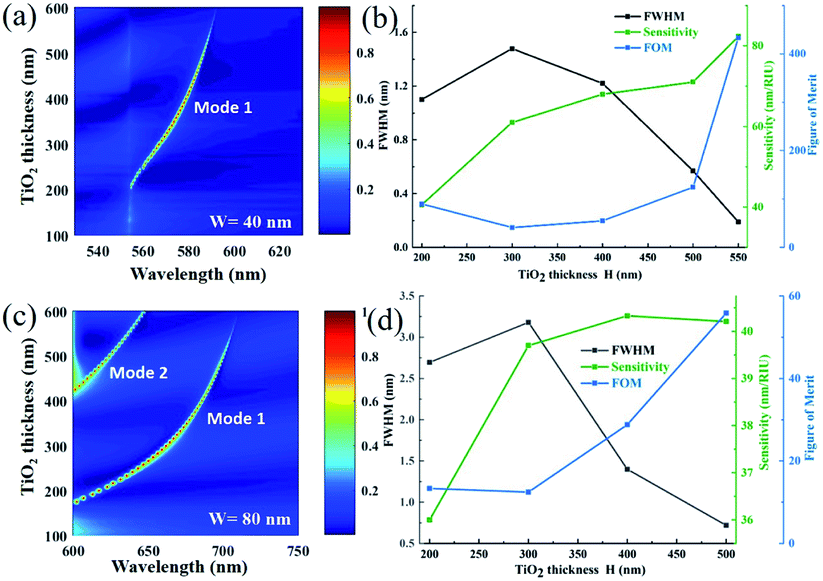 | ||
| Fig. 5 Effect of TiO2 nanostructure thickness on sensing performance. At a fixed grating width (a and b) W = 40 nm and (c and d) W = 40 nm, TiO2 thickness is a function of wavelength, and FWHM, S, and FOM are functions of TiO2 thickness. When the thickness of TiO2 changes, the other parameters are consistent with those in Fig. 1. | ||
The next parameter we explore is the TiO2 dielectric grating width (W). As W increases, the resonance peak appears redshifted, and the peak value remains almost high (Fig. 6(a)). The dependence of the resonance position on W makes the device have good tunability and will bring high manufacturing tolerances. As shown in Fig. 6(b), a small W with a narrower FWHM makes the interaction between the target molecule and the small grating width more prominent, thus improving the sensitivity of the device and obtaining a higher FOM. However, a smaller or larger W may be introduced in new resonance modes, which may interfere with the analysis of the device during actual operation. At the same time, for devices that are not tolerant of manufacturing precision, small defects are prone to cause the loss of modes. Fig. 6(c) and (d) show the dependence of the device on the structural parameter P. It can be found that the resonance wavelength shifts towards the long-wavelength direction as the period increases. In other words, the larger the period, the larger the corresponding device operating wavelength.53 Fig. 6(d) shows the FWHM of the reflection peak and the change in resonance wavelength with the period. The resonance wavelength of the structure varies linearly with the period. The black broken line shows that the FWHM widens as the period increases. A larger FWHM is detrimental to the sensing performance of the device. While trying to obtain a smaller FWHM, it is also necessary to ensure that the structure can have a higher reflection intensity. In addition, excessive reduction cycles may lead to a very small FWHM and a very large FOM. However, it is a huge challenge during the actual production of gratings, especially for instruments with low precision. It is clear from Fig. 6 that the strong dependence of the resonance wavelength position on the dielectric grating width and period indicates that the device has good tunability. However, it often has another negative effect on the actual manufacturing.54,55 It is very sensitive to equipment with low manufacturing accuracy and increases the error between the actual manufacturing and the ideal results of the simulation. In general, the optimal geometric parameters of the device should be jointly determined by its manufacturing accuracy conditions and the actual application environment.56–58
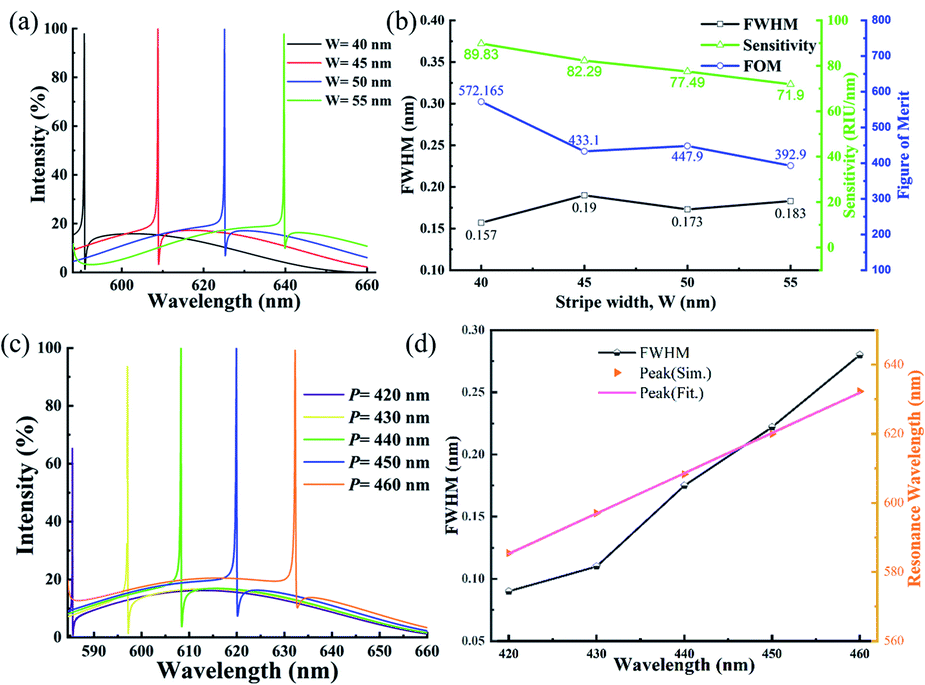 | ||
Fig. 6 The effect of TiO2 dielectric grating width (W) and period (P) on the sensing performance of the device. Under the parameters of different W: (a) simulated reflectance spectra; (b) FWHM, sensitivity (S), and figure of merit (FOM) as a function of W. Under the parameters of different P: (c) simulated reflectance spectra; (d) FWHM, and the corresponding relationship between the resonance peak and the incidence wavelength. The green point represents the resonance wavelength of the structure at different periods, and the red line represents the fitting of the point. The width of the TiO2 grating remains 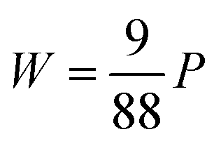 as the period changes. While changing one parameter, the other parameters remain as those in Fig. 1. as the period changes. While changing one parameter, the other parameters remain as those in Fig. 1. | ||
Finally, we investigate the tolerance of the device to the angle and polarization of incident light. The polarization insensitivity of the device is examined in more detail by scanning the polarization angle of the light source from 0° to 90°, as shown in Fig. 7(a). It can be seen that when the polarization angle increases from 0° to 90° (i.e., from TM mode to TE mode), the resonance wavelength, FWHM, and reflection intensity of the structure remain almost constant. This is an exciting result that indicates that our nanostructure is insensitive to the polarization of incident light.59–62 In addition, under TM and TE polarizations, the dependence of the working wavelength on the incidence angle has been studied, as shown in Fig. 7(b) and (c), respectively. When the incident light angle is large (30°), the device maintains a practically constant reflection intensity at an almost fixed spectral position.63,64 Because the grating unit of the device has 60° rotational symmetry, the device exhibits excellent insensitivity to polarization and tolerance to angles. Furthermore, it can be noticed that new modes appear in the TM mode when the incident light angle increases, while this does not occur in the TE mode. This may be related to the different polarization states with different effective grating lengths and the spatial distribution of the grating structures.
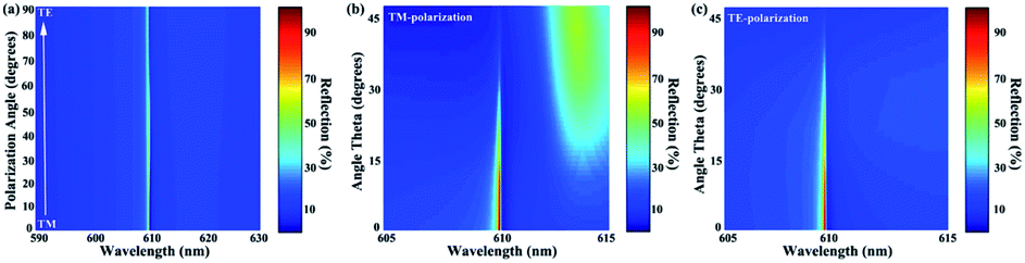 | ||
| Fig. 7 (a) Reflection pattern of the polarization angle of incident light from 0° (s, TM-polarization) to 90° (p, TE-polarization). Dependence of incident light angle on resonance wavelength under (b) TM-polarization and (c) TE-polarization. | ||
4. Conclusion
In summary, we propose a high-sensitivity refractive index sensor composed of a 2D periodic dielectric grating structure whose resonance effect is mainly excited by the guided-mode. The electromagnetic simulation results show that the optimized metasurface can excite the guided-mode resonance with an ultra-narrow linewidth of 0.19 nm. Considering the deposition of the biological medium layer on the nanostructure in actual operation, we conducted a numerical investigation of its sensing performance. When the thickness of the biological detection layer is 20 nm, the sensitivity, Q-factor, and FOM values of the nanosensor can be as high as 82.29 nm RIU−1 (nm per refractive index unit), 3207.9 and 433.1, respectively. In addition, we designed the structure to exhibit excellent polarization insensitivity and incidence angle tolerance, which is ideal because it eliminates the need for polarization and angle in the device. It is worth mentioning that compatibility with the CMOS technology is the main advantage of dielectric nanostructures over metal nanoparticle systems. This work shows that the use of low-loss all-dielectric structures is an effective way to achieve ultra-sensitive biosensing detection. The excellent performance of the guided-mode resonance sensor will also pave the way for lowering the detection limit of biosensing.Conflicts of interest
There are no conflicts to declare.Acknowledgements
This work was supported by the National Natural Science Foundation of China (11704223), the Natural Science Foundation of Fujian Province (2022J011102, 2022H0048, 2021J01972, 2021J05180, 2020J01777), and the Distinguished Young Scholars Program of Fujian Province (C18032).References
- L. Ju, B. Geng, J. Horng, C. Girit, M. Martin, Z. Hao, H. A. Bechtel, X. Liang, A. Zettl, Y. R. Shen and F. Wang, Nat. Nanotechnol., 2011, 6, 630–634 CrossRef CAS PubMed.
- S. Jahani and Z. Jacob, Nat. Nanotechnol., 2016, 11, 23–36 CrossRef CAS PubMed.
- Z. P. Zheng, Y. Zheng, Y. Luo, Z. Yi, J. G. Zhang, Z. M. Liu, W. X. Yang, Y. Yu, X. W. Wu and P. H. Wu, Phys. Chem. Chem. Phys., 2022, 24, 2527–2533 RSC.
- X. L. Wu, Y. Zheng, Y. Luo, J. G. Zhang, Z. Yi, X. W. Wu, S. B. Cheng, W. X. Yang, Y. Yu and P. H. Wu, Phys. Chem. Chem. Phys., 2021, 23, 26864–26873 RSC.
- F. Q. Zhou, F. Qin, Z. Yi, W. T. Yao, Z. M. Liu, X. W. Wu and P. H. Wu, Phys. Chem. Chem. Phys., 2021, 23(31), 17041–17048 RSC.
- M. J. Lang, P. M. Fordyce, A. M. Engh, K. C. Neuman and S. M. Block, Simultaneous, coincident optical trapping and single-molecule fluorescence, Nat. Methods, 2004, 1, 133–139 CrossRef CAS PubMed.
- T. T. Cheng, H. J. Gao, G. R. Liu, Z. S. Pu, S. F. Wang, Z. Yi, X. W. Wu and H. Yang, Colloids Surf. A Physicochem. Eng. Asp., 2022, 633(2), 127918 CrossRef CAS.
- L. X. Li, H. J. Gao, G. R. Liu, S. F. Wang, Z. Yi, X. W. Wu and H. Yang, Adv. Powder Technol., 2022, 33(3), 103481 CrossRef CAS.
- X. Lin, Y. J. Li, F. T. Chen, P. Xu and M. Li, RSC Adv., 2017, 7, 25314–25324 RSC.
- N. M. Tang, Y. J. Li, F. T. Chen and Z. Y. Han, RSC Adv., 2018, 8, 42233–42245 RSC.
- R. Magnusson and S. S. Wang, Appl. Phys. Lett., 1992, 61, 1022 CrossRef CAS.
- Z. P. Zheng, Y. Luo, H. Yang, Z. Yi, J. G. Zhang, Q. J. Song, W. X. Yang, C. Liu, X. W. Wu and P. H. Wu, Phys. Chem. Chem. Phys., 2022, 24, 8846–8853 RSC.
- N. Yu, P. Genevet, M. A. Kats, F. Aieta, J. P. Tetienne, F. Capasso and Z. Gaburro, Science, 2011, 334, 333–337 CrossRef CAS PubMed.
- N. Yu and F. Capasso, Nat. Mater., 2014, 13, 139–150 CrossRef CAS PubMed.
- H. Chen, Z. H. Chen, H. Yang, L. H. Wen, Z. Yi, Z. G. Zhou, B. Dai, J. G. Zhang, X. W. Wu and P. H. Wu, RSC Adv., 2022, 12, 7821–7829 RSC.
- J. Chen, H. Nie, C. J. Tang, Y. H. Cui, B. Yan, Z. Y. Zhang, Y. R. Kong, Z. J. Xu and P. G. Cai, Appl. Phys. Express, 2019, 12, 052015 CrossRef CAS.
- J. Homola, Chem. Rev., 2008, 108, 462–493 CrossRef CAS PubMed.
- L. Jiang, Y. Yi, Y. Tang, Z. Li, Z. Yi, L. Liu, X. Chen, R. Jian, P. Wu and P. Yan, Chin. Phys. B, 2022, 31, 038101 CrossRef.
- C. P. Liang, G. Niu, X. F. Chen, Z. G. Zhou, Z. Yi, X. Ye, T. Duan, Y. Yi and S. Y. Xiao, Opt. Commun., 2019, 436, 57–62 CrossRef CAS.
- H. Z. Zhong, Z. Q. Liu, X. S. Liu, G. L. Fu, G. Q. Liu, J. Chen and C. J. Tang, Opt. Express, 2020, 28, 37294–37306 CrossRef CAS PubMed.
- S. Wan, C. Qin, K. Wang, Y. Li, C. Guan, B. Lv, W. J. Li and J. Shi, J. Appl. Phys., 2022, 131, 213104 CrossRef CAS.
- A. I. Kuznetsov, A. E. Miroshnichenko, M. L. Brongersma, Y. S. Kivshar and B. Luk'yanchuk, Science, 2016, 354, 2472 CrossRef PubMed.
- L. Y. Jiang, Y. T. Yi, Z. Yi, H. Yang, Z. Y. Li, J. Su, Z. G. Zhou, X. F. Chen and Y. G. Yi, Acta Phys. Sin., 2021, 70, 128101 CrossRef.
- D. U. Yildirim, A. Ghobadi, M. C. Soydan, M. Gokbayrak, A. Toprak, B. Butun and E. Ozbay, J. Phys. Chem. C, 2019, 123, 19125–19134 CrossRef CAS.
- S. Xiong, Z. Yin, Y. Zhou, X. Peng, W. YFan, Z. Liu and X. Zhang, Bull. Korean Chem. Soc., 2013, 34(10), 3039–3045 CrossRef CAS.
- Y. Li, M. Li, P. Xu, S. Tang and C. Liu, Appl. Catal. Gen., 2016, 524, 163–172 CrossRef CAS.
- P. Chen, F. Liu, H. Ding, S. Chen, L. Chen and Y. J. Li, Appl. Catal. B Environ., 2019, 252, 33–40 CrossRef CAS.
- L. X. Li, X. F. Sun, T. Xian, H. J. Gao, S. F. Wang, Z. Yi, X. W. Wu and H. Yang, Phys. Chem. Chem. Phys., 2022, 24, 8279–8295 RSC.
- Y. Deng, G. Cao, Y. Wu, X. Zhou and W. Liao, Plasmonics, 2015, 10, 1537–1543 CrossRef.
- G. Cao, H. Li, Y. Deng, S. Zhan, Z. He and B. Li, Plasmonics, 2014, 9, 1163–1169 CrossRef CAS.
- F. Zhao, J. C. Lin, Z. H. Lei, Z. Yi, F. Qin, J. G. Zhang, L. liu, X. W. Wu, W. X. Yang and P. H. Wu, Phys. Chem. Chem. Phys., 2022, 24(8), 4871–4880 RSC.
- Z. Yi, J. K. Li, J. C. Lin, F. Qin, X. F. Chen, W. T. Yao, Z. M. Liu, S. B. Cheng, P. H. Wu and H. L. Li, Nanoscale, 2020, 12, 23077–23083 RSC.
- Y. Deng, G. T. Cao, H. Yang, X. Q. Zhou and Y. W. Wu, Plasmonics, 2018, 13, 345–352 CrossRef CAS.
- Y. Yang, I. I. Kravchenko, D. P. Briggs and J. Valentine, Nat. Commun., 2014, 5, 5753 CrossRef CAS PubMed.
- Y. H. Liu, M. L. Bo, X. X. Yang, P. P. Zhang, C. Q. Sun and Y. L. Huang, Phys. Chem. Chem. Phys., 2017, 19, 5304–5309 RSC.
- L. Cai, Z. H. Zhang, H. M. Xiao, S. Chen and J. L. Fu, RSC Adv., 2019, 9, 41383–41391 RSC.
- F. Long, J. Wang, Z. H. Zhang and L. Yan, J. Electroanal. Chem., 2016, 777, 58–66 CrossRef CAS.
- Z. H. Zhang, R. Cai, F. Long and J. Wang, Talanta, 2015, 134, 435–442 CrossRef CAS PubMed.
- R. Cai, W. Rao, Z. H. Zhang, F. Long and Y. L. Yin, Anal. Methods, 2014, 6, 1590–1597 RSC.
- J. Zhu, Z. Wang, S. Lin, S. Jiang, X. Liu and S. Guo, Biosens. Bioelectron., 2020, 150, 111905 CrossRef CAS PubMed.
- H. J. Chen, Z. H. Zhang, R. Cai, X. Q. Kong, X. Chen, Y. N. Liu and S. Z. Yao, Analyst, 2013, 138, 2769–2776 RSC.
- X. Lu, T. Zhang, R. Wan, Y. Xu, C. Zhao and S. Guo, Opt. Express, 2018, 26, 10179–10187 CrossRef CAS PubMed.
- J. H. Li, J. B. Jiang, Z. F. Xu, M. Q. Liu, S. P. Tang, C. M. Yang and D. Qian, Sensor. Actuator. B Chem., 2018, 260, 529–540 CrossRef CAS.
- B. Liu, S. Chen, J. Zhang, X. Yao, J. Zhong, H. Lin, T. Huang, Z. Yang, J. Zhu, S. Liu, C. Lienau, L. Wang and B. Ren, Adv. Mater., 2018, 30, 1706031 CrossRef PubMed.
- J. H. Li, J. B. Jiang, D. Zhao, Z. F. Xu, M. Q. Liu, X. Liu, H. X. Tong and D. Qian, Electrochim. Acta, 2020, 330, 135196 CrossRef CAS.
- F. Long, Z. H. Zhang, J. Wang, L. Yan and B. W. Zhou, Electrochim. Acta, 2015, 168, 337–345 CrossRef CAS.
- P. P. Lv, D. D. Xie and Z. H. Zhang, Talanta, 2018, 188, 145–151 CrossRef CAS PubMed.
- Z. Q. Liu, H. B. Shao, G. Q. Liu, X. S. Liu, H. Q. Zhou, Y. Hu, X. N. Zhang, Z. J. Cai and G. Gu, Appl. Phys. Lett., 2014, 104, 081116 CrossRef.
- G. Q. Liu, M. D. Yu, Z. Q. Liu, P. P. Pan, X. H. Liu, S. Huang and Y. Wang, Plasmonics, 2016, 11, 677–682 CrossRef CAS.
- L. Lin and Y. Zheng, Sci. Rep., 2015, 5, 14788 CrossRef CAS PubMed.
- X. Y. Lu, L. X. Zhang and T. Y. Zhang, Opt. Express, 2015, 23, 20715–20720 CrossRef CAS PubMed.
- F. Long, Z. H. Zhang, J. Wang, L. Yan, P. P. Lu and Z. X. Yang, Chin. J. Anal. Chem., 2016, 44, 908–914 CAS.
- Z. H. Cheng, J. Liao, B. Z. He, F. Zhang, F. A. Zhang, X. H. Huang and L. Zhou, ACS Sustainable Chem. Eng., 2015, 3(7), 1677–1685 CrossRef CAS.
- X. Yang, F. Zhang, Y. J. Hu, D. Z. Chen, Z. Q. He and L. Z. Xiong, Int. J. Electrochem. Sci., 2014, 9, 5061–5072 Search PubMed.
- J. K. Li, X. Chen, Z. Yi, H. Yang, Y. Tang, Y. Yi, W. Yao, J. Wang and Y. Yi, Mater. Today Energy, 2020, 16, 100390 CrossRef.
- L. X. Li, H. J. Gao, Z. Yi, S. F. Wang, X. W. Wu, R. S. Li and H. Yang, Colloids Surf. A Physicochem. Eng. Asp., 2022, 644, 128758 CrossRef CAS.
- C. Zhang, Y. T. Yi, H. Yang, Z. Yi, X. F. Chen, Z. G. Zhou, Y. G. Yi, H. L. Li, J. Chen and C. Liu, Appl. Mater. Today, 2022, 28, 101531 CrossRef.
- H. Liu, Q. Wang and F. Zhang, ACS Omega, 2020, 5, 8816–8824 CrossRef CAS PubMed.
- W. X. Cao, L. Lin, H. F. Qi, Q. He, Z. J. Wu, A. Q. Wang, W. H. Luo and T. Zhang, J. Catal., 2019, 373, 161–172 CrossRef CAS.
- W. H. Luo, W. X. Cao, P. C. A. Bruijnincx, L. Lin, A. Q. Wang and T. Zhang, Green Chem., 2019, 21, 3744–3768 RSC.
- X. Lin, M. Li, Y. J. Li and W. Chen, RSC Adv., 2015, 5, 105227–105238 RSC.
- X. Lin, S. W. Du, C. H. Li, G. J. Li, Y. J. Li, F. T. Chen and P. F. Fang, Catal. Lett., 2020, 150, 1898–1908 CrossRef CAS.
- Y. Zheng, P. H. Wu, H. Yang, Z. Yi, Y. Luo, L. Liu, Q. J. Song, M. Pan, J. G. Zhang and P. G. Cai, Opt Laser. Technol., 2022, 150, 108002 CrossRef CAS.
- X. Z. Zhu, Y. Z. Cheng, J. P. Fan, F. Chen, H. Luo and L. Wu, Diam. Relat. Mater., 2022, 121, 108743 CrossRef CAS.
| This journal is © The Royal Society of Chemistry 2022 |