
 Open Access Article
 This Open Access Article is licensed under a Creative Commons Attribution-Non Commercial 3.0 Unported Licence
Key factors for ultra-high on/off ratio thin-film transistors using as-grown carbon nanotube networks†
Yun Sun‡
ab,
Pengpeng Li‡ab,
Esko I. Kauppinenc,
Dong-Ming Sun *ab and
Yutaka Ohno*d
*ab and
Yutaka Ohno*d
aShenyang National Laboratory for Materials Science, Institute of Metal Research, Chinese Academy of Sciences, 72 Wenhua Road, Shenyang, 110016, China. E-mail: dmsun@imr.ac.cn
bSchool of Material Science and Engineering, University of Science and Technology of China, 72 Wenhua Road, Shenyang, 110016, China
cDepartment of Applied Physics, Aalto University School of Science, PO Box 15100, FI-00076 Aalto Espoo, Finland
dDepartment of Quantum Engineering, Nagoya University, Furo-cho, Chikusa-ku, Nagoya 464-8603, Japan. E-mail: yohno@nuee.nagoya-u.ac.jp
First published on 1st June 2022
Abstract
Approximately 30% of as-grown carbon nanotube (CNT) networks are metallic, usually leading to a trade-off between carrier mobility and on/off ratio in CNT thin-film transistors (TFTs). Figuring out the key factors of ultra-high on/off ratio in CNT TFTs should be considerably essential for the development of large-scale electronic devices in the future. Here ultra-high on/off ratios of 107–108 are realized for CNT TFTs with mobility of ∼500 cm2 V−1 s−1. We propose that one of the key factors to achieve the high on/off ratio is a clean CNT thin film without charge traps and doping due to residual dispersant used in conventional solution processes. Moreover, on/off ratio degradation under operation voltage is significantly suppressed by decreasing the diameter of CNTs.
Introduction
Networks of single-walled carbon nanotubes (CNTs) have attracted much attention as an active layer in thin-film transistors (TFTs).1 Such a thin-film material exhibits uniform properties by averaging properties of individual CNTs, providing a route to practical uses of CNT-based electronics systems. The CNT TFTs are expected to enable a fabrication of high-performance integrated circuits for flexible and transparent devices on a plastic film, using relatively simple techniques such as solution,2,3 printing,4 and sheet transfer processes.5–7One of the important issues of CNT TFTs to be addressed is to improve the on/off ratio. As-grown CNT networks usually contain metallic CNTs of 30%, which lead to a trade-off between carrier mobility and on/off ratio in CNT TFTs.1,8 Many techniques have been developed to eliminate the drawbacks of metallic nanotubes,9–14 for instance, solution-processed techniques, such as density gradient ultracentrifugation (DGU)15 and gel filtration technique,16 are representative to separate metallic and semiconducting CNTs effectively. Nowadays, the purity of semiconducting CNTs above 99% have been achieved with the help of state-of-the-art polymer-sorted DGU,17–20 and the resultant CNT TFTs exhibit on/off ratio around 108 with mobility of 297 cm2 V−1 s−1.17 But the scalability of solution-processed CNT film should be an inevitable issue for their applications in large-scale flexible electronic devices compared with the meter-scale and roll-to-roll as-grown CNT films,21 even though the fabrication of CNT TFTs is wafer-scale across 200 mm silicon substrates right now.22 On the other hand, the selective growth of semiconducting CNTs directly is another route to fabricate high-performance CNT devices,23 but the poor reproducibility and rigorous synthesis condition would be dealt with urgently in the future. Therefore, figuring out the key factors about improving the on/off ratio in TFTs using as-grown CNT networks could be helpful and prospective for the development of large-scale CNT-based electronic devices in the future.
In the previous work,7 we reported a gas-phase filtration and transfer process to fabricate the CNT TFTs exhibiting the carrier mobility of 634 cm2 V−1 s−1 and the on/off ratio of 6 × 10⁶. Here using the devices with high on/off ratio, we investigate the causes of degradations of on/off ratio of CNT TFTs for various cases, such as the residual dispersant, chemical doping and CNT diameter. Then through the systematic characterization and analysis, we clarify that key factors to realize ultra-high on/off ratios in CNT TFTs should be a clean CNT thin film without charge traps and doping. In addition, CNTs with smaller diameters are quite competent for restraining the on/off degradation under operation voltage. Finally, CNT TFTs with on/off ratio around 108 are realized with the mobility of ∼500 cm2 V−1 s−1 simultaneously, providing a bright path for the fabrication of high-performance CNT electronic devices.
Results and discussion
The back-gate CNT TFTs used in this study were fabricated on a p+-Si substrate with a thermally-oxidized SiO2 layer of a thickness of 100 nm, by a gas-phase filtration and transfer process. The details of growth and fabrication process have been reported in ref. 7. Fig. 1 shows transfer characteristics of a typical CNT TFT fabricated by the gas-phase filtration and transfer process. The device showed p-type characteristics with the on/off ratio of 5 × 10⁸ and mobility of 496 cm2 V−1 s−1 evaluated at the linear region by a rigorous model (ESI S1†).24 The CNT TFTs simultaneously show both a high mobility and a high on/off ratio. In the previous report,7 we clarified that the high mobility originated from the unique morphology of the CNT network, that is, the network of long CNTs connected by Y-junctions, by which the number of inter-CNT junctions along the current flow paths and the junction resistances were reduced. At a larger source-drain voltage (VDS = −5 V), the minority electron current slightly increases at off state, resulting in a degradation of the on/off ratio. | ||
| Fig. 1 Typical transfer characteristics (ID–VGS) of CNT TFTs. The channel length (Lch) and channel width (Wch) are both 100 μm, the thickness of dielectric layer (SiO2) is 100 nm. The on/off ratio decreases from 5 × 10⁸ to 2 × 10⁷ with |VDS| increasing from 0.5 to 5 V. | ||
On/off ratios of CNT TFTs fabricated by different techniques are summarized in Table 1. The typical on/off ratios of the TFTs in this work are between 106 and 108 at VDS = −0.5 V, even though the on/off ratio decreased by one to two orders of magnitude at VDS = −5 V, which is still smaller than those reported in the previous literature.4–6,15 It should be noted that the on/off ratio of CNT TFTs depends on the drain bias because the off current increases with the drain field due to the minority carrier injection from the drain electrode, and that the on/off ratio should be considered at a drain bias under a realistic operation condition. The degradation of on/off ratio under the operation condition seriously increases power consumption of the circuits, such as logic large-scale integrated circuits (LSIs) and active matrices of flat-panel displays. Therefore, how on/off ratio depends on the fabrication technique and drain bias voltage should be comprehended thoroughly.
| Reference | Low VDS | High VDS | Diameter of CNTs (nm) | CNT synthesis | TFT fabrication | ||
|---|---|---|---|---|---|---|---|
| VDS (V) (average drain field (V m−1)) | On/off | VDS (V) (average drain field (V m−1)) | On/off | ||||
| This work (1.1 nm) | −0.5 (5 × 10³) | 106–108 | −5 (5 × 10⁴) | 105–107 | 1.1 | Floating-catalyst CVD | Dry process |
| This work (1.6 nm) | −0.5 (5 × 10³) | 106–108 | −5 (5 × 10⁴) | 103–106 | 1.6 | Floating-catalyst CVD | Dry process |
| Cao et al.5 | −0.5 (5 × 10³) | ∼104 | −5 (5 × 10⁴) | 80 | ∼1.5 | Supported-catalyst CVD | Dry transfer, CNT strips |
| Ha et al.4 | −0.1 (2 × 10³) | ∼105 | −1 (2 × 10⁴) | 400 | ∼1.4 | Arc discharge | Solution, DGU |
| Engel et al.15 | −0.1 (5 × 10⁴) | 104 | −3 (1.5 × 10⁶) | 300 | 1.3–1.7 | Arc discharge | Solution, DGU |
First, we studied the cause of low on/off ratio of solution-based CNT TFTs. In the solution process, surfactants such as sodium-dodecyl-sulfate (SDS) and sodium-cholate are used to disperse and stabilize CNTs in water.25,26 However, it is difficult to remove such surfactants completely from CNTs after the device fabrication. In this study, we investigate the effect of surfactant by soaking CNT TFTs in 1% water solution of SDS. Fig. 2a shows transfer characteristics of a CNT TFT before and after soaking in the SDS solution. The on/off ratio decreased from 3 × 10⁶ to 4 × 10². The threshold voltage shifted towards positive VGS, from −5 V to −1 V, this means that the SDS has an ability to dope positive carriers, i.e. holes, in CNTs. Such doping effect of SDS has been also observed by XPS and Raman spectroscopy, exhibiting the electron-withdrawing sulfate group as a strong p-dopant.27 Moreover, the subthreshold slope (s-factor) increased from 0.35 V dec−1 to 1.2 V dec−1 indicating the charge trapping effect of SDS molecules. The effective trap density per area is estimated as 3.59 × 1011 cm−2 eV−1 (ESI S2†). The mechanism of the degradation of on/off ratio due to the charge trapping effect is schematically shown in Fig. 2b. Under an existence of traps around the CNTs, charges are captured by the traps with increasing VGS, so that the modulation effect of VGS is restricted. Consequently, the TFTs exhibiting the poor VGS dependence cannot be turned on or off completely, and the on/off ratio decreases. This phenomenon has been often observed in ID–VGS characteristics of solution-based TFTs.28–31 The decrease in the on/off ratio can be related to both the carrier doping and the charge trapping effects.
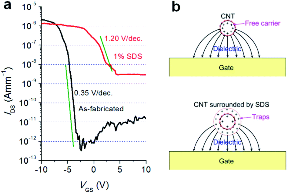 | ||
| Fig. 2 Charge trapping effect of the SDS solution on the CNT TFT. (a) On/off ratio degraded from 3 × 10⁶ to 4 × 10² after 1% SDS solution treatment. (b) Schematics of the charge trapping effect of the SDS solution. | ||
As a matter of fact, when the concentration of surfactants increase, more traps will be introduced and surround CNTs, while more charge carriers will be captured by these traps with the increased VGS leading to the more serious restriction of gate modulation. Similarly, when the ion size of surfactants increase, the capability of capturing charge carriers for one trap will be also enhanced, leading to the increased amounts of trapped charge carriers in all traps.
We investigate the effect of chemical doping on the on/off ratio of CNT TFTs. Fig. 3a shows the change in transfer characteristics by the chemical doping on the CNT TFTs. The chemical doping was carried out by spin coating of the toluene solution of tetrafluorotetracyano-p-quinodimethane (F4TCNQ), which is a p-type dopant for CNTs on CNT TFTs.29,32 With increasing the concentration of F4TCNQ, the on/off ratio decreased, and the threshold voltage shifted toward the direction of positive VGS, similar to the case of SDS treatment. Fig. 3b shows the schematics of the F4TCNQ doping on the CNT TFT. There are a number of current paths in the CNT thin film, and the drain current of the CNT TFT is the sum of the currents of each path. Even though each path has a large on/off ratio, the on/off ratio of total current can be decreased if the threshold voltage is different for each path due to the electron current at the off state. Such a fluctuation of threshold voltage was observed for the single-CNT channel FETs after the chemical doping with F4TCNQ, without significant decrease in on/off ratio (ESI S3†). In the solution-based chemical doping, the dopant molecules would inhomogeneously stick onto the surface of CNTs, so that, the shift of threshold voltage fluctuates. Consequently, the on/off ratio decreases for the multiple current-path transistors such as CNT TFTs, although that of the single-CNT channel FET does not change significantly.
 | ||
| Fig. 3 Chemical doping effect of the F4TCNQ on the CNT TFT. (a) Threshold voltage shifted after the doping of the toluene solution of F4TCNQ with various concentrations. (b) Schematics of chemical doping effect of F4TCNQ. | ||
The barrier for the electron injection can be related to the degradation of the on/off ratio at high drain voltage, since the increase in off current is mainly due to the minority electron current as shown in Fig. 1. In the case of semiconducting CNTs, the diameter determines the energy bandgap, and thus the Schottky barrier for an electron between the metallic and semiconducting CNTs as well as the CNTs and metal electrodes.33–36 It was reported that the CNTs with the diameter of 1.0–2.2 nm are capable of providing a good on/off ratio.37 However, the on/off ratios decrease 2–3 orders of magnitude under a higher VDS for the CNTs with the diameter of 1.5 nm, 1.4 nm and 1.3–1.7 nm,4–6 the on/off ratios of TFTs would be lower than 1000 under practical operation bias, as shown in Table 1.
Fig. 4 shows the on/off ratios of TFTs fabricated by the gas-phase filtration and transfer process for two average diameters of CNTs: (a) 1.1 nm and (b) 1.6 nm. The average diameters were determined from the absorption spectra.38,39 Both types of CNT TFTs showed similar performance including the carrier mobility and on/off ratio at VDS of −0.5 V. However, the on/off ratios exhibited different degree of degradation at a higher VDS of −5 V. The on/off ratio decreased from 3 × 10⁸ to 2 × 10⁷ for an average CNT diameter of 1.1 nm and from 2 × 10⁸ to 3 × 10⁵ for 1.6 nm. The electron current increased by one order of magnitude for 1.1 nm CNTs and by three orders of magnitude for 1.6 nm CNTs at VDS = −5 V. Furthermore, the statistical data regarding the degree of on/off ratio degradation are shown in Fig. 4c and d for 1.1 and 1.6 nm CNTs, respectively. We measured thirty devices for each type of TFTs. For 1.1 nm CNTs, 24% (70%) of devices show the on/off ratio greater than 108 (107) at VDS = −0.5 V, and 19% (60%) of devices greater than 108 (107) for 1.6 nm CNTs. The on/off ratio degraded 1–2 orders of magnitude for 1.1 nm CNTs, which is much smaller than 2–4 orders for 1.6 nm CNTs. A number of 1.1 nm CNT TFTs exhibited very small on/off ratio degradation (less than 10). This indicates that the on/off ratio degradation phenomenon can significantly be improved by using the smaller-diameter CNTs. Theoretically, the energy bandgap Eg of the semiconducting CNT is inversely proportional to the nanotube diameter d, that is, Eg = 2γ0aC–C/d ≈ 0.78/d (eV), where γ0 is the tight-binding overlap energy for a carbon–carbon bond and aC–C is the nearest carbon–carbon bond distance.34,35,40 The energy bandgap value Eg of 1.1 nm and 1.6 nm CNTs are ∼0.71 eV and ∼0.49 eV, respectively. From the schematic band diagrams as shown in the insets in Fig. 4a and b, it is visible that more electrons can tunnel through the barrier from the drain electrode to semiconducting CNTs, due to the thinner barrier caused by the smaller Eg of 1.6 nm CNT TFT. This leads to the electron current increase and the on/off ratio decrease.
 | ||
| Fig. 4 Distribution of on/off ratio degradation for the CNT TFTs. (a) and (b) Typical ID–VGS characteristics of the TFTs, at VDS of −0.5 and −5 V, for the CNTs with diameter of 1.1 and 1.6 nm, respectively. The insets show schematic band diagrams of electron tunneling for 1.1 and 1.6 nm CNTs, respectively. (c) and (d) On/off ratio distributions for 1.1 and 1.6 nm CNTs, respectively. | ||
In addition, bundling of CNTs can also degrade the on/off ratio of CNT TFTs because there is an unfavorable electrostatic shielding effect to frustrate gate modulation of the associated semiconducting CNTs if the bundle consists of at least one metallic CNT. The bundle behaves as an electrically metallic wire, leading to reductions in the on/off ratio of TFTs.41 Therefore, it is preferred to use the individual CNTs rather than thick bundles to form the CNT networks. The networks in the present study consist predominantly of individual nanotubes and a few small bundles, which contributes to the high on/off ratio of TFTs.
Admittedly, the fabrication procedure in this work is similar with the one as described previously,7 but here we primarily intend to provide a full comprehension and analysis on the key factors that can influence the current on/off ratio of thin-film transistors using as-grown CNT network significantly. Although the fabrication processes and corresponding performance seem to have no significant improvement besides of the post-annealing process, the ultimate goal of these two works are different from each other.
Conclusions
In summary, we realized the high on/off ratios of 107–109 for the CNT TFTs using a gas-phase filtration and transfer process. The on/off ratio degradation at the high VDS is suppressed with the smaller diameter CNTs. We also investigated the on/off ratio degradation phenomenon by the contaminations from surfactants and chemical doping. In order to realize high on/off ratio, it is well-known to control the density of metallic CNTs lower than the percolation threshold; in this letter, the other two key factors are pointed out: (1) reduce trapping and doping effects by using the clean CNTs as the active layer; (2) select the smaller diameter (∼1.1 nm) CNTs to suppress the on/off ratio degradation.Conflicts of interest
There are no conflicts to declare.Acknowledgements
This work was supported by the National Natural Science Foundation of China (62125406), the National Key Research and Development Program of China (2021YFA1200013), the Key-Area Research and Development Program of Guangdong Province (2019B010934001), the Strategic Priority Research Program of Chinese Academy of Sciences (XDB30000000), the Key Research Program of Frontier Sciences of the Chinese Academy of Sciences (ZDBS-LY-JSC027), R&D promotion scheme funding international joint research promoted by National Institute of Information and Communications Technology (NICT), Japan, and the Aalto University MIDE program via the CNB-E project and partially supported by the Academy of Finland (Pr. No. 128445).References
- E. S. Snow, J. P. Novak, P. M. Campbell and D. Park, Appl. Phys. Lett., 2003, 82, 2145–2147 CrossRef CAS.
- M. C. LeMieux, M. Roberts, S. Barman, Y. W. Jin, J. M. Kim and Z. Bao, Science, 2008, 321, 101–104 CrossRef CAS PubMed.
- C. Wang, J. Zhang and C. Zhou, ACS Nano, 2010, 4, 7123–7132 CrossRef CAS PubMed.
- M. Ha, Y. Xia, A. A. Green, W. Zhang, M. J. Renn, C. H. Kim, M. C. Hersam and C. D. Frisbie, ACS Nano, 2010, 4, 4388–4395 CrossRef CAS PubMed.
- Q. Cao, H. Kim, N. Pimparkar, J. P. Kulkarni, C. Wang, M. Shim, K. Roy, M. A. Alam and J. A. Rogers, Nature, 2008, 454, 495–500 CrossRef CAS PubMed.
- W. J. Yu, S. Y. Lee, S. H. Chae, D. Perello, G. H. Han, M. Yun and Y. H. Lee, Nano Lett., 2011, 11, 1344–1350 CrossRef CAS PubMed.
- D. M. Sun, M. Y. Timmermans, Y. Tian, A. G. Nasibulin, E. I. Kauppinen, S. Kishimoto, T. Mizutani and Y. Ohno, Nat. Nanotechnol., 2011, 6, 156–161 CrossRef CAS PubMed.
- C. Kocabas, N. Pimparkar, O. Yesilyurt, S. J. Kang, M. A. Alam and J. A. Rogers, Nano Lett., 2007, 7, 1195–1202 CrossRef CAS PubMed.
- Y. Li, D. Mann, M. Rolandi, W. Kim, A. Ural, S. Hung, A. Javey, J. Cao, D. Wang, E. Yenilmez, Q. Wang, J. F. Gibbons, Y. Nishi and H. Dai, Nano Lett., 2004, 4, 317–321 CrossRef CAS.
- Y. Ono, S. Kishimoto, Y. Ohno and T. Mizutani, Nanotechnology, 2010, 21, 205202 CrossRef PubMed.
- P. G. Collins, M. S. Arnold and Ph. Avouris, Science, 2001, 292, 706–709 CrossRef CAS PubMed.
- Y. Zhang, Y. Zhang, X. Xian, J. Zhang and Z. Liu, J. Phys. Chem. C, 2008, 112, 3849–3856 CrossRef CAS.
- L. M. Gomez, A. Kumar, Y. Zhang, K. Ryu, A. Badmaev and C. Zhou, Nano Lett., 2009, 9, 3592–3598 CrossRef CAS PubMed.
- L. An, Q. Fu, C. Lu and J. Liu, J. Am. Chem. Soc., 2004, 126, 10520–10521 CrossRef CAS PubMed.
- M. Engel, J. P. Small, M Steiner, M Freitag, A. A. Green, M. C. Hersam and Ph Avouris, ACS Nano, 2008, 2, 2445–2452 CrossRef CAS PubMed.
- T. Tanaka, H. Jin, Y. Miyata and H. Kataura, Appl. Phys. Express, 2008, 1, 114001 CrossRef.
- F. Hennrich, W. Li, R. Fischer, S. Lebedkin, R. Krupke and M. M. Kappes, ACS Nano, 2016, 10, 1888–1895 CrossRef CAS PubMed.
- Y. Li, M. Zheng, J. Yao, W. Gong, Y. Li, J. Tang, S. Feng, R. Han, Q. Sui, S. Qiu, L. Kang, H. Jin, D. Sun and Q. Li, Adv. Funct. Mater., 2022, 32, 2107119 CrossRef CAS.
- T. Lei, L. L. Shao, Y. Q. Zheng, G. Pitner, G. Fang, C. Zhu, S. Li, R. Beausoleil, H.-S. P. Wong, T. C. Huang, K. T. Cheng and Z. Bao, Nat. Commun., 2019, 10, 2161 CrossRef PubMed.
- L. Liu, J. Han, L. Xu, J. Zhou, C. Zhao, S. Ding, H. Shi, M. Xiao, L. Ding, C. Jin, Z. Zhang and L. M. Peng, Science, 2020, 368, 850–856 CrossRef CAS PubMed.
- B. W. Wang, S. Jiang, Q. B. Zhu, Y. Sun, J. Luan, P. X. Hou, S. Qiu, Q. W. Li, C. Liu, D. M. Sun and H. M. Cheng, Adv. Mater., 2018, 30, 1802057 CrossRef PubMed.
- M. D. Bishop, G. Hilles, T. Srimani, C. Lau, D. Murphy, S. Fuller, J. Humes, A. Ratkovich, M. Nelson and M. M. Shulaker, Nat. Electron., 2020, 3, 492–501 CrossRef CAS.
- Z. Zhu, N. Wei, W. Cheng, B. Shen, S. Sun, J. Gao, Q. Wen, R. Zhang, J. Xu, Y. Wang and F. Wei, Nat. Commun., 2019, 10, 4467 CrossRef PubMed.
- Q. Cao, M. Xia, C. Kocabas, M. Shim and J. A. Rogers, Appl. Phys. Lett., 2007, 90, 023516 CrossRef.
- M. J. O'Connell, S. M. Bachilo, C. B. Huffman, V. C. Moore, M. S. Strano, E. H. Haroz, K. L. Rialon, P. J. Boul, W. H. Noon, C. Kittrell, J. Ma, R. H. Hauge, R. B. Weisman and R. E. Smalley, Science, 2002, 297, 593–596 CrossRef PubMed.
- N. R. Tummala and A. Striolo, ACS Nano, 2009, 3, 595–602 CrossRef CAS PubMed.
- K. R. Moonoosawmy and P. Kruse, J. Am. Chem. Soc., 2010, 132, 1572–1577 CrossRef CAS PubMed.
- Y. Miyata, K. Shiozawa, Y. Asada, Y. Ohno, R. Kitaura, T. Mizutani and H. Shinohara, Nano Res., 2011, 4, 963–970 CrossRef CAS.
- T. Takenobu, T. Kanbara, N. Akima, T. Takahashi, M. Shiraishi, K. Tsukagoshi and H. Kataura, Adv. Mater., 2005, 17, 2430–2434 CrossRef CAS.
- Q. Cao, S. H. Hur, Z. T. Zhu, Y. Sun, C. Wang, M. A. Meitl, M. Shim and J. A. Rogers, Adv. Mater., 2006, 18, 304–309 CrossRef CAS.
- C. Wang, J. C. Chien, K. Takei, T. Takahashi, J. Nah, A. M. Niknejad and A. Javey, Nano Lett., 2012, 12, 1527–1533 CrossRef CAS PubMed.
- Y. Nosho, Y. Ohno, S. Kishimoto and T. Mizutani, Nanotechnology, 2007, 18, 415202 CrossRef.
- R. Saito, G. Dresselhaus and M. S. Dresselhaus, Physical Properties of Carbon Nanotubes, Imperial College Press, London, 1998 Search PubMed.
- J. W. Mintmire and C. T. White, Carbon, 1995, 33, 893–902 CrossRef CAS.
- J. W. G. Wildöer, L. C. Venema, A. G. Rinzler, R. E. Smalley and C. Dekker, Nature, 1998, 391, 59–62 CrossRef.
- Z. Chen, J. Appenzeller, J. Knoch, Y. Lin and P. Avouris, Nano Lett., 2005, 5, 1497–1502 CrossRef CAS PubMed.
- S. Salamat, X. Ho, J. A. Rogers and M. A. Alam, IEEE Trans. Nanotechnol., 2011, 10, 439–444 Search PubMed.
- Y. Tian, M. Y. Timmermans, S. Kivisto, A. G. Nasibulin, Z. Zhu, H. Jiang, O. G. Okhotnikov and E. I. Kauppinen, Nano Res., 2011, 4, 807–815 CrossRef CAS.
- Y. Tian, H. Jiang, J. V. Pfaler, Z. Zhu, A. G. Nasibulin, T. Nikitin, B. Aitchison, L. Khriachtchev, D. P. Brown and E. I. Kauppinen, J. Phys. Chem. Lett., 2010, 1, 1143–1148 CrossRef CAS.
- Y. Asada, F. Nihey, S. Ohmori, H. Shinohara and T. Saito, Adv. Mater., 2011, 23, 4631–4635 CrossRef CAS PubMed.
- T. Kim, G. Kim, W. I. Choi, Y. K. Kwon and J. M. Zuo, Appl. Phys. Lett., 2010, 96, 173107 CrossRef.
Footnotes |
| † Electronic supplementary information (ESI) available. See https://doi.org/10.1039/d2ra02088b |
| ‡ These authors were equal major contributors to this work. |
| This journal is © The Royal Society of Chemistry 2022 |