
 Open Access Article
 This Open Access Article is licensed under a Creative Commons Attribution-Non Commercial 3.0 Unported Licence
Potential transition and post-transition metal sulfides as efficient electrodes for energy storage applications: review
Thirunavukarasu Kajana
 *abc,
Arumugam Pirashanthan
ac,
Dhayalan Velauthapillai
*c,
Akila Yuvapragasam
c,
Shivatharsiny Yohi
b,
Punniamoorthy Ravirajan
a and
Meena Senthilnanthanan
*b
*abc,
Arumugam Pirashanthan
ac,
Dhayalan Velauthapillai
*c,
Akila Yuvapragasam
c,
Shivatharsiny Yohi
b,
Punniamoorthy Ravirajan
a and
Meena Senthilnanthanan
*b
aClean Energy Research Laboratory, Department of Physics, University of Jaffna, Jaffna, Sri Lanka. E-mail: tskajana@gmail.com
bDepartment of Chemistry, University of Jaffna, Jaffna, Sri Lanka. E-mail: meena@univ.jfn.ac.lk
cFaculty of Engineering and Science, Western Norway University of Applied Sciences, Bergen, Norway. E-mail: Dhayalan.Velauthapillai@hvl.no
First published on 20th June 2022
Abstract
Electrochemical energy storage has attracted much attention due to the common recognition of sustainable energy development. Transition metal sulfides and post-transition metal sulfides have been intensively been focused on due to their potential as electrode materials for energy storage applications in different types of capacitors such as supercapacitors and pseudocapacitors, which have high power density and long cycle life. Herein, the physicochemical properties of transition and post-transition metal sulfides, their typical synthesis, structural characterization, and electrochemical energy storage applications are reviewed. Various perspectives on the design and fabrication of transition and post-transition metal sulfides-based electrode materials having capacitive applications are discussed. This review further discusses various strategies to develop transition and/or post-transition metal sulfide heterostructured electrode-based self-powered photocapacitors with high energy storage efficiencies.
 Kajana Thirunavukarasu | Kajana Thirunavukarasu received her BSc (Hons.) degree with specialization in Chemistry from University of Jaffna, Sri Lanka in 2017. She is now completing her Master of Philosophy degree (MPhil) in Chemistry at University of Jaffna, Sri Lanka. Her research interest focuses on photocapacitors for solar energy harvesting and storage, and supercapacitor applications. She is now pursuing a research internship at Western Norway University of Applied Sciences, Norway. |
 Arumugam Pirashanthan | Pirashanthan Arumugam received his BSc (Hons.) degree with specialization in Physics from South Eastern University of Sri Lanka, Sri Lanka in 2017. He is now completing his Master of Philosophy (MPhil) degree in Physics at University of Jaffna, Sri Lanka. His research interest is in the area of Hybrid Polymer Photovoltaics and Photoresponsive nanomaterials for energy conversion. He is now pursuing a research internship at Western Norway University of Applied Sciences, Norway. |
 Dhayalan Velauthapillai | Dhayalan Velauthapillai received his Cand.Mag (1988), Cand.Scient (1991), and PhD- Dr.Scient (1996) degrees in Physics and Technology from the University of Bergen, Norway. He did his Post Doc (1999–2001) at University of Neuchâtel, Switzerland and University of Bergen, Norway. He is associated with Western Norway University of Applied Sciences since 2001 as Professor in Physics and Technology. His research interests are in the field of electromagnetic waves and clean energy technologies. His research is focused on mathematical modelling, computer simulation, synthesis, characterization of advanced nanomaterials with particular emphasis on emerging solar cell, hydrogen production, and energy storage technologies. |
 Akila Yuvapragasam | Akila Yuvapragasam received her PhD degree in the field of solar cells from Anna University, India in 2017. She has done her post-doctoral fellowship in the field of hybridizing DSSC and supercapacitors. Her research focus is towards solar energy-based supercapacitors and photocapacitors. |
 Yohi Shivatharsiny | Shivatharsiny Yohi is a senior lecturer at the Department of Chemistry, University of Jaffna, Sri Lanka. She obtained her Master's degree (MS) and doctoral degree (PhD) from the University of South Dakota, USA. Her research interest is in the area of hydrogen production through water splitting and environmental remediation using different nanomaterials. She has received several awards and honors for her research and academic activities. |
 Punniamoorthy Ravirajan | Punniamoorthy Ravirajan received his BSc (Hons.) degree with specialization in Physics from University of Jaffna, Sri Lanka in 1994 and MSc degree in Physics from University of Peradeniya, Sri Lanka in 1999. He obtained his PhD degree in Physics at Imperial College, London in 2004. After a postdoctoral period there, he returned to University of Jaffna, Sri Lanka, where he was promoted to Senior Lecturer in Physics in 2005 and then to Professor in Physics with effect from 2009. He is now serving as Senior Professor in Physics with effect from 2017. His research interest focuses on the optimization of organic photovoltaic devices. |
 Meena Senthilnanthanan | Meena Senthilnanthanan received her BSc (Hons.) degree with specialization in Chemistry from University of Jaffna, Sri Lanka in 1993. Then, she joined Prof. Ronald Grigg's group in University of Leeds, United Kingdom to pursue postgraduate studies and obtained her PhD degree in organic chemistry in 2000. She has been associated with University of Jaffna since 2013 as an associate professor in Chemistry. She is now serving as Professor in Chemistry. Her research interest focuses on nanomaterials in energy conversion and photocatalysis. |
1. Introduction
Solar energy is one of the well-known abundant energy sources for the development of clean energy technology to meet the future global energy demand. Its development and the respective technological enhancement are crucial to address the emerging environmental problems associated with the current use of fossil fuels1–3 as the proposed energy conservation/storage devices shall be cost-effective, and more reliable with integrated generation of sources and reduced environmental impacts.4–8 Moreover, an improved energy storage system is essential for the efficient utilization of solar, hydro, and wind energies.9–11 Such energy storage devices could be used in various applications with specific requirements. Parameters such as energy efficiency, power density, response time, cost with economic scale, and lifetime determine the most suitable type of device for an application.12Commonly, the produced energy can be stored by two different approaches using batteries and capacitors.13,14 Batteries convert and store the electrical energy as chemical energy; however, capacitors store the electrical energy as received. The power of a battery is controlled by an electrochemical process.15–17 Further, the limited lifetime, power density, weak self-discharge, and use of hazardous chemicals are considered major drawbacks of batteries.18–20 Capacitors can be categorized into conventional capacitors, supercapacitors, and photocapacitors based on their purposes/properties. Conventional capacitors can only store very limited energy.21,22 However, supercapacitors provide high levels of electrical power and possess a long operational lifetime.23–29 The above capacitors are mostly used to provide short bursts of power in buses and cranes, and hold much promise for electric vehicles and the green grid. Besides, the research on self-powered photocapacitors is of much interest in current trends due to their free energy conversion from the sun and its self-charging properties.11,30–35
2. Photocapacitors
For the sake of completeness, we choose to explain the fundamentals of photocapacitors, which is quite a new thematic area. The good growth of research on photocapacitors aims at the future of replacing batteries with self-charged solar photocapacitors in many smart electronic devices. Photocapacitors can harvest solar energy and store it in the form of electrical energy, and are expected to solve the problem of the unstable power output of solar cells under intermittent sunlight. These photocapacitor architectures mainly belong to the integrated structures of solar cells with supercapacitors and/or heterostructured photoactive electrodes with energy storing materials. The first photocapacitor architecture with a specific capacitance of 0.69 F cm−2 was reported in 2004 by integrating dye sensitized solar cell with supercapacitor structures. This sandwich-type electrochemical device consisted of a photoelectrode, a redox-free liquid electrolyte, and a counter electrode. The photoelectrode consisted of dye-adsorbed semiconductive nanoparticles and a porous layer of activated carbon, whereas the counter electrode also contained a porous activated carbon layer.30 Thereafter, several research works were reported with integrated architectures.36–38 However, the heterostructured photocapacitors are of great interest due to the direct contact between the photoactive and storage materials, making the working electrode itself a light absorber and an energy storage device through an oxidation process. This heterostructured photocapacitor possesses the unique synergistic coupling of photoactive materials and a transition metal sulfide to drive the transition metal oxide derived from its sulfide to act as a capacitive platform via redox pseudocapacitance under illumination.Fig. 1 represents the working mechanism of a heterostructured photocapacitor. Further, Fig. 1a depicts the photocharging process, which is mediated by three steps. The electrons in the valence band of a semi-conducting photoactive material absorb solar energy (in step 1) and get excited to the conduction band by leaving positive holes behind (in step 2). Simultaneously, these positive holes are captured (in step 3) by the storage material through an oxidation process; thus, the system gets charged. These charged particles, positive holes and negative electrons, are free charge carriers that can mediate electrical current flow through the device when it is connected to a circuit; thus, the system gets discharged, as shown in Fig. 1b.39,40
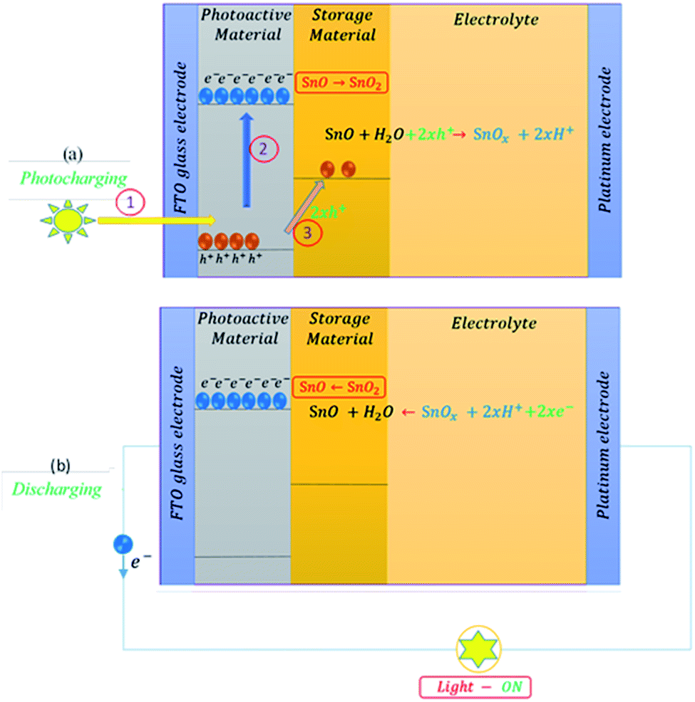 | ||
| Fig. 1 Working mechanism of a self-powered photocapacitor representing the photocharging process (a) and discharging process (b). | ||
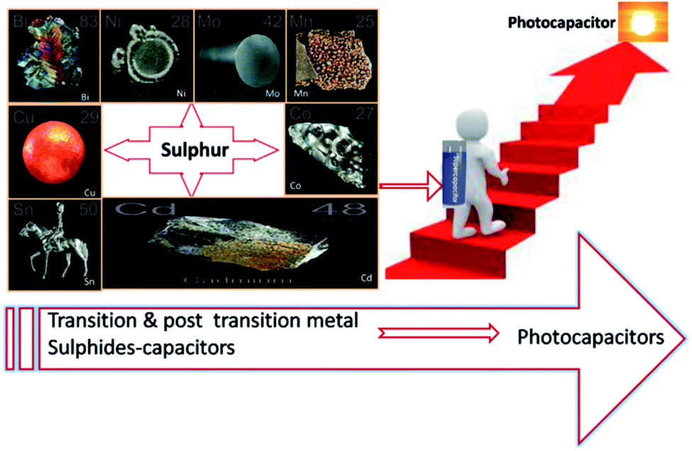
In the past few years, transition metal sulfide-based nanomaterials have been extensively studied in supercapacitors,41–43 solar cells,44,45 hydrogen production,46 lithium-ion batteries,47 and catalytic48,49 applications. Furthermore, transition and post-transition metal sulfides (TMSs) have attracted attention due to their potential as pseudocapacitive materials for capacitors owing to their high specific capacitance, low cost, large global abundance,50–54 greater conductivity than their oxide and hydroxide counterparts,55,56 and rich redox reactions. In this scenario, a promising BiVO4–PbOx heterostructured photocapacitive system was reported with a specific capacitance of 6 mF cm−2 at a high open circuit potential of 1.5 V vs. reversible hydrogen electrode (RHE). Here, BiVO4 and PbOx nanoparticles were employed as photoactive and capacitive layers, respectively. The PbOx structure was derived from the controlled oxidation of colloidal PbS quantum dots.57 However, the toxicity of PbS is of concern; research studies are currently focusing on replacing PbS with non-toxic materials. Recently, a novel heterostructured system with carbon sheet/Ag2MoO4–SnS/Pt was reported with a specific capacitance of 340 F g−1 and an open circuit potential of 1.25 V vs. Ag/AgCl electrode. Here, the Ag2MoO4 and SnO nanoparticles served as photoactive and capacitive layers, respectively.58 The SnO nanoparticles were derived from the controlled oxidation of spherical SnS nanoparticles. The high capacitance is attributed to the large conductive surface and high conductivity of the Ag2MoO4–SnS film. The above reported studies with PbS and SnS metal sulphides evidence the energy storage ability in heterostructured photocapacitors. Even though only two of the above papers were published with these types of heterostructured photocapacitors, other transition and post-transition metal sulfides also have potential to be used in these photocapacitors. Therefore, this article reviews the latest advances in transition and post-transition metal sulfides-based capacitors, focusing on their synthesis, characterization, and electrochemical energy storage behaviors. This review will be useful for building research in the field of photocapacitors. The schematic diagram for the outlook on photocapacitors from supercapacitors is shown in Fig. 2.
 | ||
| Fig. 2 Outlook for photocapacitors from supercapacitors. | ||
3. Synthesis of transition and post-transition metal-sulfides
Transition and post-transition metal sulfides have been synthesized by various chemical methods such as solvothermal (ST), hydrothermal (HT), electrodeposition (ED), chemical bath deposition (CBD), microwave-assisted synthesis (MWA), wet chemical synthesis, hot injection method, successive ionic layer adsorption and reaction (SILAR), sulfurization, and chemical vapor deposition (CVD). This review mainly focuses on solvothermal, hydrothermal, electrodeposition, chemical bath deposition, microwave-assisted synthesis, wet chemical synthesis, and hot injection methods.Table 1 summarizes various methods for synthesizing transition and post-transition metal sulfides based on bismuth (Bi), copper (Cu), cobalt (Co), cadmium (Cd), manganese (Mn), tin (Sn), molybdenum (Mo), and nickel (Ni).
| Material | Method | Precursors | Solvent | Conditions | Morphology | Ref. | |
|---|---|---|---|---|---|---|---|
| 1 | Bi2S3 | ST | Bi(NO3)3·5H2O and C2H5NS | Water, ethylene glycol, and butyldiglycol | 24 h at 150 °C | Sphere-like Bi2S3 nanoparticles | 59 |
| Bi2S3–rGO | HT | GO, Bi(NO3)3·5H2O, and C2H5NS | Water | 8 h at 160 °C | Bi2S3 nanorods on rGO nanosheets | 60 | |
| Bi2S3 | Bi(NO3)3·5H2O and CH4N2S | Ethylene glycol | 10 h at 140 °C | Nanorods | 61 | ||
| Bi2S3/graphene | Wet chemical synthesis | GO, BiCl3, and CTAB | Dimethylformamide (DMF) | 3 h at 200 °C | Nanorods | 62 | |
| 2 | CuS | ST | Cu(NO3)2·3H2O and sulfur | Ethylene glycol | 24 h at 150 °C | Nanosheets | 63 |
| Polypyrrole (PPy), copper nitrate hydrate, and CH4N2S | Glycol | 24 h at 150 °C | Microspheres | 64 | |||
| [Bmim]2Cu2Cl6 and CH4N2S | Absolute ethanol | 20 h at 100 °C | 3D hierarchical microspheres | 65 | |||
| CuS/MWCNT | HT | MWCNT, Cu(NO3)2·3H2O, and CH4N2S | Ethylene glycol | 72 h at 180 °C | Nanosheets | 66 | |
| CuS | Cu(CH3COO)2·H2O, CH4N2S, CTAB, and NaOH | Double-distilled (DD) water | 20 h at 130 °C | Granular nanostructures | 67 | ||
| CuS/Ni foam | CuCl2·2H2O, sulfur powder, and Cu powder | Ethanol | 12 h at 80 °C | Nanosheets | 68 | ||
| CuS thin films | CuSO4·5H2O and C2H5NS | Deionized water (DI water) | 50 min at 70 °C | Flower-like morphology | 69 | ||
| CuS/CCs (CSCCs) | CuSO4·5H2O and CH4N2S | Ethylene glycol | 4 h at 180 °C | 3D flower-like microspheres made up of nanosheets | 70 | ||
| 3 | Co1−xS | ST | Co(CH3COO)2·4H2O and C3H7NO2S | Diethanolamine | 12 h at 200 °C | Flower-like architectured nanosheets | 71 |
| CoS1.097 | CoCl2·6H2O and C3H7NO2S | Ethylene glycol | 18 h at 180 °C | Nanotubes | 72 | ||
| CoS2 | Co(CH3COO)2·4H2O and CS2 | Ethylenediamine | 18 h at 200 °C | Yolk–shell and double-shell to hollow structures | 73 | ||
| CoS2–rGO | Co(NO3)2·6H2O and Na2S2O3 | DI water and ethylene glycol | 9 h at 180 °C | CoS2 nanoparticles on RGO nanosheets | 74 | ||
| CoS2 | HT | CoCl2·6H2O, sodium citrate, and C2H5NS | DI water and ethanol | 0.5–9 h at 160–200 °C | 3D hollow CoS2 cubic structures | 75 | |
| rGONF/CoS2 | GO, thiourea, and Co(CH3COO)2·4H2O | Ethanol | 10 h at 200 °C | — | 76 | ||
| CCs/CoS2 | (Co(OH)(CO3)0.5·xH2O and sulfur powder | DI water | 5 h at 110 °C | Nanowires | 77 and 78 | ||
| CoS2/MWCNT | MWCNT, Co(NO3)2·6H2O, and C3H7NO2S | DI water | 18 h, 150 °C | — | 79 | ||
| Co9S8/3DG | Glucose, graphene, CoCl2, and CH4N2S | Ethanol and DI water | 12 h at 180 °C | Nanoparticles | 80 | ||
| Co3S4/rGO | GO, CoCl2·6H2O, CH4N2O, and Na2S | DI water | 8 h at 120 °C | Nanoflakes | 81 | ||
| Co3S4/NF | Co3O4 and CH3CSNH2 | DI water | 0.5–14 h at 120 °C | Nanosheets | 82 | ||
| CoS | CoCl2·6H2O, urea, and Na2S·9H2O | DI water | 8 h at 180 °C | Nanotubes | 83 | ||
| CoCl2·6H2O, glycerol, and C2H5NS | Isopropanol and ethanol | 5 h at 120 °C | Hierarchical porous nanospheres | 84 | |||
| CoS/NF | ED | CoCl2·6H2O and CH4N2S | NH4OH (aq) | — | Nanosheets | 85 | |
| CoS/eRG/Ni foam | CoCl2·6H2O and CH4N2S | HCl (aq) | 180 s | 86 | |||
| CoS/NF | CBD | CoCl2·6H2O and CH4N2S | Water/ethanol | 4 h at 90 °C | Nanoflakes and tapioca sago like nanoparticles | 50 | |
| CoS/NF | MWA | CoCl2·6H2O, C6H8O7, and C2H5NS | Ethylene glycol | 5 min at 700 W | 3D flower-like hierarchitecture | 87 | |
| CoS | Co(CH3COO)2·4H2O and C2H5NS | Ethanol | 5 min at 120 °C | Hollow nanoprisms | 88 | ||
| CoSx | Wet chemical synthesis | Co(CH3COO)2 and Na2S·9H2O | DI water | — | — | 89 | |
| CoS | Hot injection method | C9H18N2O2S2 and CoCl2·6H2O | Methanol and acetone | 2 h at 200 and 260 °C | Nanoplatelets | 90 | |
| 5 | CdS/Ni foam | HT | Cd(CH3COO)2·2H2O and CH4N2S | DI water | 1 h at 80 °C | Nanoparticles | 91 |
| 6 | γ-MnS/rGO | HT | GO, MnCl2, and Na2S | DI water | 12 h at 180 °C | Nanorods | 92 |
| 7 | m-SnS2 | HT | Na2MoO4, SnCl4·5H2O, and C3H7NO2S | DI water | 24 h at 200 °C | Leaf-like nanosheet | 93 |
| O–SnS | CBD | SnCl2 and Na2S2O3 | Double distilled water | 2–6 h at 343 K | Nanoflower-like structures | 94 and 95 | |
| 8 | C/MoS2 | HT | Glucose and (NH4)2MoS4 | DI water | 24 h at 200 °C | — | 96 |
| MoS2 | Na2MoO4·2H2O and C3H7NO2S | DI water | 48 h at 180 °C | Nanosheet-like structures | 97 | ||
| (NH4)2MoO4 and CH4N2S | DI water | 15 h at 150 °C | Sphere-like nanostructures | 98 | |||
| (NH4)6Mo7O24·4H2O and CH4N2S | — | 8–24 h at 200 °C | 3D flower-like microspheres composed of nanosheets | 99 | |||
| Na2MoO4·2H2O and CH4N2S | DI water | 1–8 h at 200 °C | Nanosheets | 100 | |||
| MoO3·H2O and C2H5NS | DI water | 24 h at 200 °C | Sponge | 101 | |||
| Na2MoO4·2H2O and H2NCSNH2 | DI water | 24 h at 200 °C | Flower-like mesoporous structures | 102 | |||
| (NH4)6Mo7O24 and SC(NH2)2 | Water | 24 h at 210 °C | 103 | ||||
| MoS2/Mo foil | CVD and ED | Mo foil and sulfur powder | Oxalic acid, Na2SO4, and NaF | 0.5–2 h at 200–300 °C | Sponge-like structures | 104 | |
| 9 | Ni3S2 | HT | Ni(NO3)2·6H2O and CH4N2S | DI water | 16 h at 120 °C | 3D nanosheets | 105 |
| Ni3S2/NF | Ni foam and CH4N2S | DI water and ethanol | 8 h at 115, 140, 165 °C | Nanosheets and nanorods | 106 | ||
| Ni foam and C2H5NS | DI water and ethanol | 6 h at 120, 150, 180 °C | 3D hierarchical dendrites | 107 | |||
| 2–8 h at 120 °C | |||||||
| CNT@Ni3S2 | CNTs, Ni(NO3)2, and Na2S | DI water and ethanol | 12 h at 160 °C | Nanosheets | 108 | ||
| NiS/C-dot | Lemon juice, NiSO4, and CH4N2S | DI water | 24 h at 200 °C | Hierarchical flower-like nanostructure | 109 | ||
| α-NiS | C4H14NiO8 and CH4N2S | DI water | 12 h at 160 °C | Hollow spheres | 110 | ||
| β-NiS | 12 h at 200 °C | ||||||
| NiS | Ni(NO3)2, Na3C6H5O7, C6N6K3Co, and Na2S | DI water and ethanol | 6 h at 100 °C | Hollow frame-like particles constructed with nanocubes | 111 | ||
| Ni3S2/NF | ED | NiCl2·6H2O and CH4N2S | DI water | — | Nanoflakes | 112 | |
| Nickel sulfide/ERGO | Graphite, NiCl2·6H2O, and CH4N2S | DI water | — | — | 113 | ||
| NiS/Ti foil | CBD | Ni(NO3)2·6H2O and CH4N2S | Ethanol | 4 h at 70 °C | Nanorods/nanoplates | 114 | |
| NiS2/NF | MWA | Ni(NO3)2, CH4N2S, and polyvinylpyrrolidone K-30 (PVP) | DI water | 2–4 h at 150 °C | Nanocubes, nanospheres, and nanoparticles | 115 |
4. Structural characterization of transition and post-transition metal-sulfides
X-Ray Diffraction (XRD), Scanning Electron Microscopy (SEM), and X-ray Photoelectron Spectroscopy (XPS) are the important characterization techniques that have widely been used to characterize nanomaterials referred to in Table 1, and are discussed in this section.4.1. Powder X-ray diffraction (XRD)
This technique is used to study the crystalline nature (phase and crystal size) of nanomaterials. Fig. 3 illustrates the XRD patterns of Bi2S3 obtained using different solvent mixtures including water. In all the XRD patterns of Bi2S3 samples shown in Fig. 3, the diffraction peaks are observed at 2θ values of 15.65°, 17.55°, 22.35°, 23.70°, 25.20°, 27.35°, 28.60°, 31.80°, 33.00°, 33.90°, 35.60°, 39.00°, 40.10°, 45.60°, 46.55°, 52.75°, 59.20°, 62.60°, 65.05°, and 69.60°. These peaks can be ascribed to the reflections due to (200), (120), (220), (101), (310), (130), (211), (221), (410), (311), (240), (041), (430), (440), (501), (312), (640), (152), (721), and (651) planes of the orthorhombic phase of Bi2S3. The intensity of the peaks varies with different solvent systems. The most crystalline Bi2S3 was obtained in the butyldiglycol/water (BG/W) system among all the solvent systems studied.59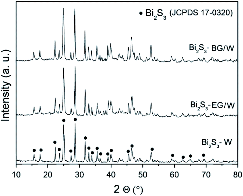 | ||
| Fig. 3 XRD patterns of Bi2S3 samples in different solvent systems.59 | ||
Peng et al. have reported the preparation of CuS using polypyrrole (PPy). Fig. 4 represents the XRD patterns of the as-prepared CuS, PPy, and CuS@PPy composite. All the indexed peaks can be assigned to CuS, which confirms the crystalline structure of CuS with a hexagonal phase.64
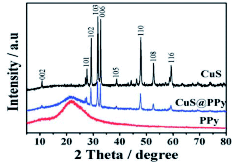 | ||
| Fig. 4 XRD patterns of CuS, PPy, and CuS@PPy composite.64 | ||
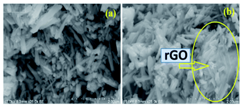
Chen et al. reported the XRD patterns of the reduced graphene oxide on Ni foam (rGONF)/CoS2 nanocomposite and bare CoS2 nanoparticles, as shown in Fig. 5. The diffraction peaks at 27.9°, 32.3°, 36.2°, 39.8°, 46.3°, 54.9°, 57.6°, 60.2°, and 62.7° can be indexed to (111), (200), (210), (211), (220), (311), (222), (023), and (321) planes of CoS2. Besides, some other diffraction peaks were assigned to the (111), (311), (222), (511), and (440) planes of Co9S8. However, no peaks of rGO were found in the XRD pattern of the rGONF/CoS2 nanocomposite due to the very small quantity of rGO and the strong diffraction density of CoS2.76
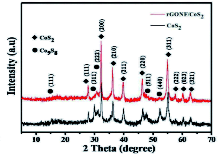 | ||
| Fig. 5 XRD patterns of the bare CoS2 nanoparticles and the rGONF/CoS2 nanocomposite.76 | ||
Fig. 6 depicts the XRD patterns of SnS thin films at different reaction times of 120 (TS1), 240 (TS2), and 360 (TS3) min. The (013) plane shows a highly intense peak among the (011), (012), (102), (110), (013), (104), (022), and (115) crystalline planes, which were well matched with JCPDS card no. 00-001-0984. It was found that the detected peak positions and crystal planes belong to the formation of the orthorhombic structure of the prepared SnS (O-SnS) thin films. Further, at the reaction time of 240 min, strong diffraction peaks were observed at (013), (104), and (115) planes.95
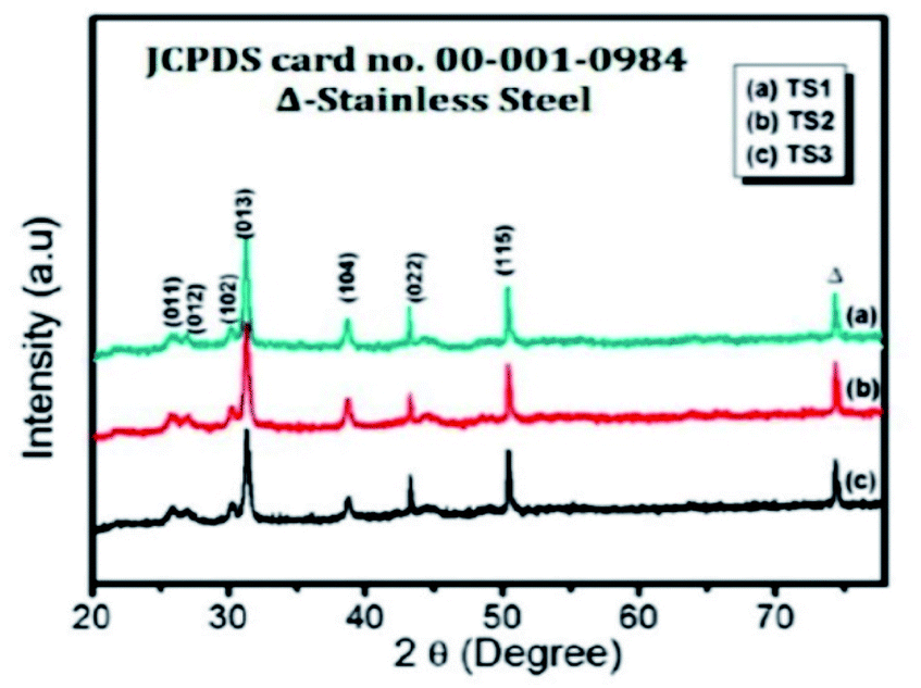 | ||
| Fig. 6 XRD patterns of SnS thin films at reaction times of 120 (TS1), 240 (TS2), and 360 (TS3) min.95 | ||
The XRD patterns of self-synthesized MoS2 samples were studied by Hu et al.,96 Huang et al.,97 and Wang et al.,99 which could be readily indexed to the hexagonal phase of MoS2, consistent with the standard powder diffraction file of MoS2 (JCPDS 37-1492). The four main diffraction peaks at 14.2°, 32.5°, 35.8°, and 55.4° correspond to the (002), (100), (102), and (106) planes of MoS2, which match well with the JCPDS card no. 75-1539.
Fig. 7 represents the XRD pattern of NiS thin film on titanium (Ti) foil substrate synthesized by the CBD method.114 The well-defined diffraction peaks of the as-synthesized NiS are clear evidence of its polycrystalline nature. Moreover, the diffraction peaks at 29.90°, 34.22°, and 45.3° correspond to (100), (101), and (102) planes, respectively, which shows a perfect match with the JCPDS card no. 02-1273 of NiS. The XRD peaks of Ti foil substrate are labeled with a star (*) in Fig. 6, and the average crystallite size calculated along the highly preferred (102) plane using the well-known Scherrer's relation [D = 0.9λ/β![[thin space (1/6-em)]](https://www.rsc.org/images/entities/char_2009.gif) cosθ] is 19 nm.
cosθ] is 19 nm.
 | ||
| Fig. 7 XRD pattern of NiS thin film on titanium (Ti) foil.114 | ||
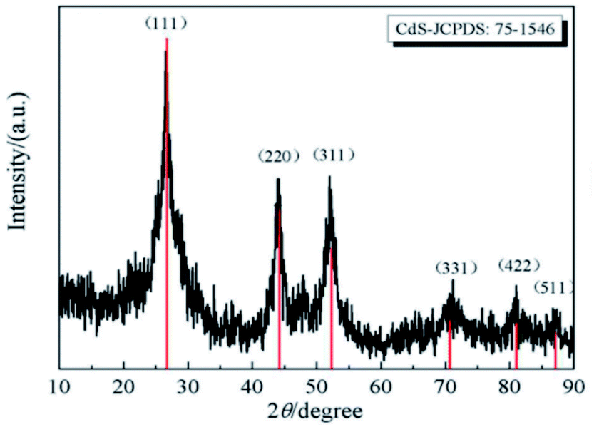
Xu et al.91 reported the synthesis of CdS powder by CBD, and its XRD pattern is displayed in Fig. 8. The XRD pattern well matches with the standard cubic CdS (JCPDS card no. 75-1546). The observed diffraction peaks at 2θ of 26.5°, 43.9°, 52.1°, 70.5°, 80.8°, and 86.9° correspond to the planes of (111), (220), (311), (331), (422), and (511), respectively. The lattice constants were calculated to be a = b = c = 0.5822 nm for the sample and compared with the standard values of CdS (a = b = c = 0.5820 nm). According to Scherrer's relationship, the average crystallite size of CdS was calculated to be 17 nm.
 | ||
| Fig. 8 XRD pattern of CdS powder.91 | ||
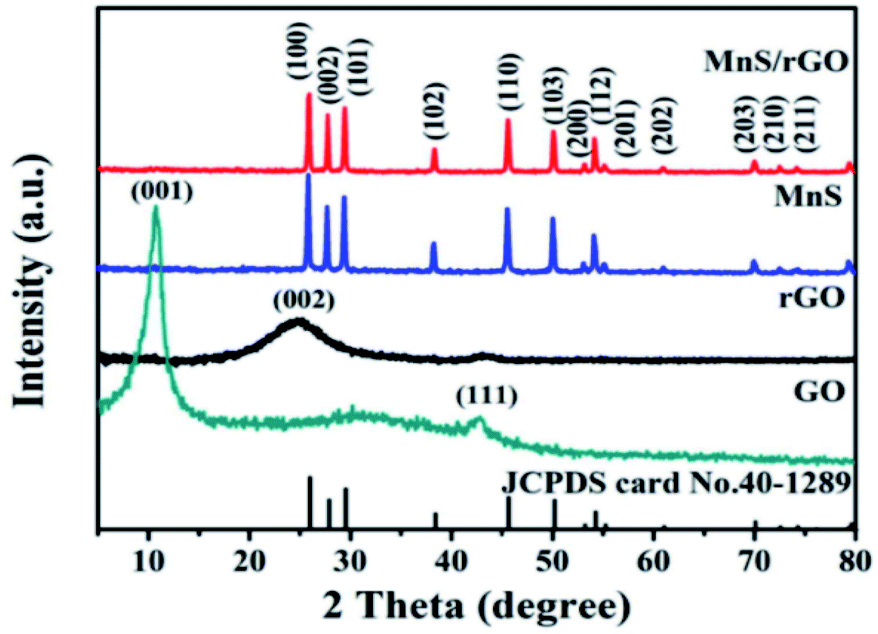
The XRD patterns of the GO, rGO, pure γ-MnS, and γ-MnS/rGO composite, synthesized by Zhang et al. through the hydrothermal method, are shown in Fig. 9. The diffraction planes of γ-MnS are (100), (002), (101), (102), (110), (103), (200), (112), (201), (202), (203), (210), and (211), which match well with its 2θ values (JCPDS no. 40-1289). The synthesized γ-MnS is fairly pure because the XRD spectrum does not show any peaks that correspond to other materials. However, the diffraction peaks found for the γ-MnS/rGO composite are inconsistent with that of pure γ-MnS. Further, the diffraction peak position of 25° for rGO is not clearly noted due to the low stacking degree and fairly even dispersion of rGO in the as-synthesized composite.92
 | ||
| Fig. 9 XRD patterns of GO, rGO, γ-MnS, and γ-MnS/rGO.92 | ||
4.2. Field emission scanning electron microscopy (FESEM)
FESEM is used to understand the surface morphologies of the transition and post-transition metal sulfides. Fig. 10a–c depicts the surface morphologies of the samples of orthorhombic SnS (O-SnS) thin films prepared at TS1, TS2, and TS3 (120, 240, and 360 min). The FESEM images of all the films show that O-SnS nanostructures have been homogeneously grown throughout the surface of the film. It can be seen that the surface morphology differs with the deposition time as nanoflakes at TS1, nanoflowers at TS2, and nanogranules at TS3.94,95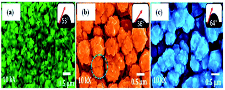 | ||
| Fig. 10 FESEM images of O-SnS thin films prepared at (a) TS1 (120 min), (b) TS2 (240 min), and (c) TS3 (360 min).94,95 | ||
Fig. 11 shows the surface morphologies of (a) GO, (b) rGO, (c) pure γ-MnS, and (d) γ-MnS/rGO-60 composite. It was observed that many wrinkles of rGO sheets were coated on the γ-MnS surfaces and interlaced with each other. Moreover, the presence of rGO impacts the morphology of MnS, i.e., the γ-MnS/rGO-60 composite shows a nanoparticle-assembled rod structure as a result of rGO coated on MnS nanoparticles restraining the aggregation and limiting the rod growth.92
 | ||
| Fig. 11 SEM images of (a) GO, (b) rGO, (c) pure γ-MnS, and (d) γ-MnS/rGO-60 composite.92 | ||
Fig. 12a depicts the low-magnification SEM image of CdS spheres directly grown on Ni foam through the hydrothermal method. Electrolyte penetration is facilitated with the CdS/Ni foam, which possesses a 3D grid structure with hierarchical macroporosity. Fig. 12b and c show the higher magnification SEM images of CdS/Ni foam electrode, which reveals that the average diameter of CdS sphere is about 2 μm. As seen in the further enlarged Fig. 12d, the CdS microsphere is tremelloid.91
 | ||
| Fig. 12 SEM images of CdS/Ni foam electrode at different magnifications of (a) ×370, (b) ×1000, (c) ×3000 and (d) ×10000.91 | ||
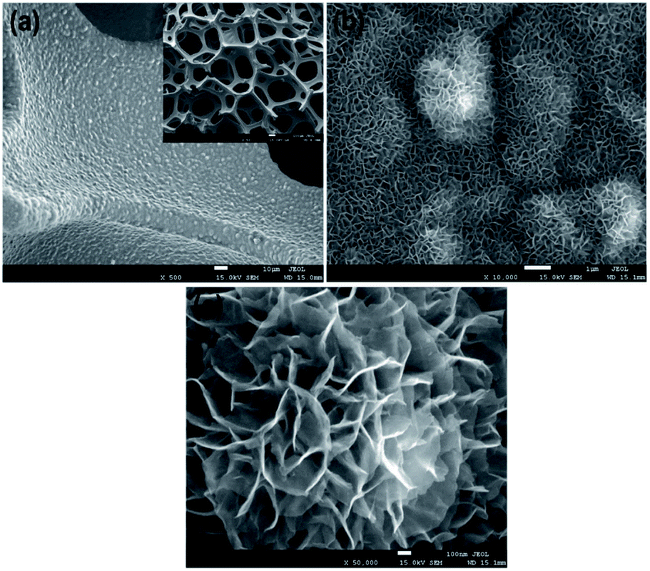
The FESEM surface morphology of the NiS thin film deposited on Ti foil by Gaikar et al. is shown in Fig. 13. The NiS film possesses a uniformly distributed network of nanorods over the Ti foil substrate with several air voids. The diffusion of electroactive species is made effective due to the open vacant space between the nanorods/nanoplates during the intercalation/de-intercalation process. Hence, the shrinkage of internal resistance of the nanomaterial takes place, which enhances its capacitive performance.114
 | ||
| Fig. 13 FESEM image of NiS thin film on Ti foil.114 | ||
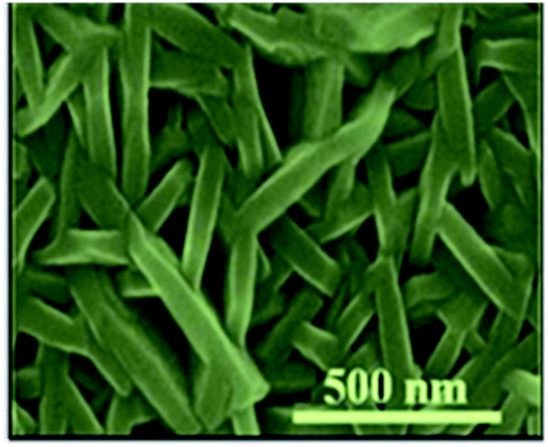
Fig. 14 shows the typical SEM images of pure Bi2S3 and Bi2S3–graphene (BG) composite. Pure Bi2S3 with an irregular rod-like structure and an average size of 40–70 nm can be observed in Fig. 14a. Fig. 14b shows that the rGO sheets in the composite are not perfectly flat and display a crumbled and rippled structure. The individually grown Bi2S3 nanorods on rGO ensure that each nanorod participates in the electrochemical process of the energy storage system.62
 | ||
| Fig. 14 FESEM images of (a) Bi2S3 and (b) BG composite.62 | ||
Fig. 15a represents the NiS2 nanoparticles with a size of 50 nm, which were obtained after 30 min of microwave irradiation. The NiS2 nanospheres between the size of 50 and 150 nm were observed after 2 h of microwave irradiation, and are shown in Fig. 15b. Further, 3 h of microwave irradiation produce imperfect NiS2 nanocubes, as shown in Fig. 15c, while perfect and uniform NiS2 nanocubes were successfully obtained as shown in Fig. 15d with 4 h of microwave irradiation.115
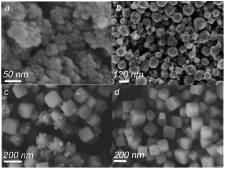 | ||
| Fig. 15 SEM images of NiS2 after microwave irradiation for different time durations: (a) 30 min, (b) 2 h, (c) 3 h, and (d) 4 h.115 | ||
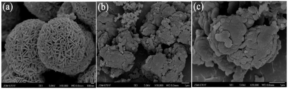
Fig. 16 shows a uniformly grown thin film of CoS with high density on the Ni foam, forming a 3D hierarchical structure, as illustrated in the inset of Fig. 16a. In the higher magnification images of Fig. 16b and c, the CoS thin films on the Ni foam exhibit a characteristic morphology composed of interlaced nanosheets.85
 | ||
| Fig. 16 FESEM images of CoS on Ni foam substrate at (a) low, (b and c) higher magnifications.85 | ||
The SEM image of CuS in Fig. 17a indicates that the prepared CuS consists of uniform spheres with an average diameter of 1 μm, and these microspheres are composed of several intertwined sheet-like subunits. Fig. 17b and c correspond to the CuS@PPy composite, in which an aggregate of PPy on individual CuS microspheres exhibits a rough surface.64
 | ||
| Fig. 17 SEM images of (a) CuS, (b and c) CuS@PPy composite at low and high magnifications.64 | ||
4.3. X-ray photoelectron spectroscopy (XPS)
The exterior and synthetic states of the molecules within the prepared sample were evaluated using XPS. The wide scan XPS spectrum of the orthorhombic SnS (O-SnS) thin film deposited in 240 min is shown in Fig. 18a. Peaks of the spectrum are assigned to Sn 3d3/2, Sn 3d5/2, S 2p3/2, C 1s, and O 1s states. The Sn 3d spectrum, which is shown in Fig. 18c, exhibits two main peaks corresponding to Sn 3d5/2 and Sn 3d3/2 states that are positioned at 486.5 and 495 eV, respectively. The energy separation among these two peaks is about ∼8.5 eV, which matches well with the reported value in the literature;116 this designates Sn in the SnS phase and +2 oxidation state. In addition to these main peaks, the S 2p3/2 state is observed at 168.6 eV, as shown in Fig. 18b. This confirms the occurrence of the pure O-SnS phase in the film layers.95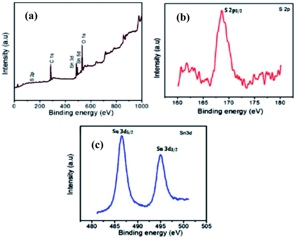 | ||
| Fig. 18 XPS spectrum of O-SnS thin film (a) survey scan spectrum, (b) S 2p, and (c) Sn 3d core level.95 | ||
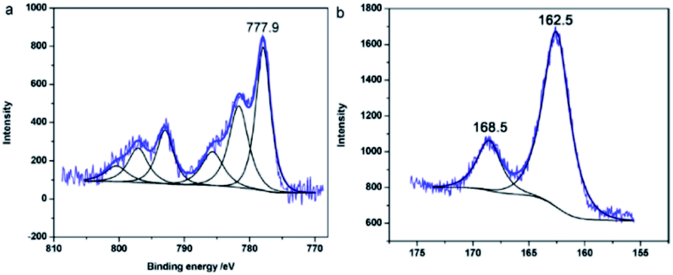
Fig. 19 depicts the XPS spectra of CoS-interlaced nanosheets, which were synthesized via a facile microwave-assisted (MWA) method.87 Fig. 19a shows the Co 2p spectrum, whereas the main peaks located at the lower binding energy value of 777.9 eV and higher binding energies are assigned to Co2+ in CoS. Fig. 19b shows that the binding energy value of the S 2p state is about 162.5 eV, which indicates that most of the S species exist as S2− in the product, as reported in the literature.85 Moreover, the peak at 168.5 eV represents the O impurity.
 | ||
| Fig. 19 XPS spectra of (a) Co 2p and (b) S 2p of CoS.87 | ||
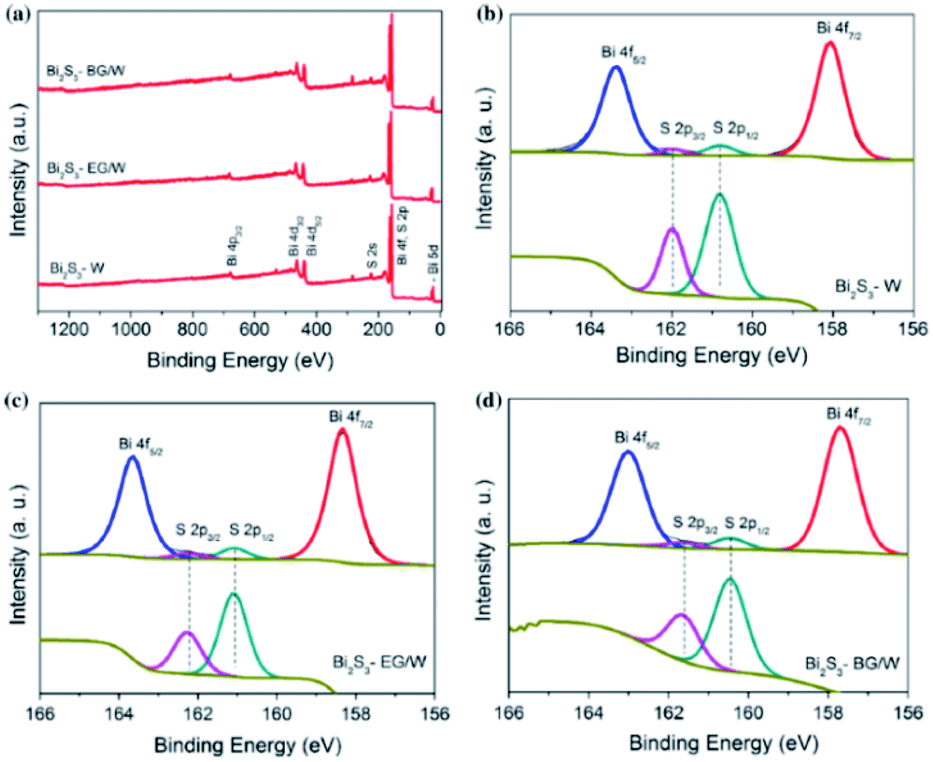
Fig. 20 represents the chemical states of Bi2S3, which were investigated by high-resolution Bi 4f and S 2p XPS spectra. Fig. 20a depicts the overall spectrum of Bi2S3 in water, ethylene glycol/water, and butyl glycol/water. The Bi 4f spectrum of Bi2S3–W (water) in Fig. 20b shows two predominant peaks at 158.1 and 163.4 eV, which correspond to the spin states of Bi 4f7/2 and Bi 4f5/2, respectively, in Bi2S3. The Bi 4f spectra of the other samples show peaks at 158.3 and 163.6 eV for Bi2S3–EG/W (ethylene glycol/water) as in Fig. 20c, and peaks at 157.7 and 163 eV for Bi2S3–BG/W (butyl glycol/water) as in Fig. 20d. The peak positions in Fig. 19 match well with the binding energy values reported in the literature for Bi3+.117 The magnified core-level S 2p spectrum is shown below the Bi 4f region for each Bi2S3 sample. The S 2p region consists of two asymmetric peaks. The signal with a higher intensity located at about 162 eV is ascribed to S 2p3/2 and the smaller signal at about 160.7 eV is attributed to the spin state of S 2p1/2. The S 2p peaks are at 162 and 160.8 eV for Bi2S3–W, 161.6 and 160.5 eV for Bi2S3–EG/W, and 162.2 and 161.1 eV for Bi2S3–BG/W. The positions of the S 2p3/2 and S 2p1/2 signals in the S 2p spectra prove that sulfur exists in its S2− valence state.59
 | ||
| Fig. 20 XPS spectra of Bi2S3 (a) survey scan spectrum and high-resolution Bi 4f and S 2p spectra of (b) Bi2S3–W, (c) Bi2S3–EG/W, and (d) Bi2S3–BG/W.59 | ||
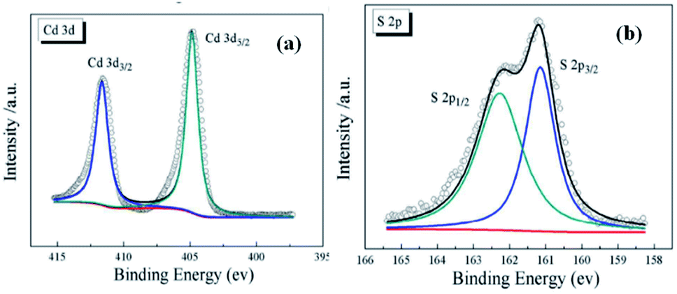
Xu et al.91 evaluated the valence states of Cd and S in CdS samples using XPS, where CdS was synthesized through the hydrothermal method. The existence of cadmium in its Cd2+ state was confirmed by the presence of the two peaks at 405.2 eV for Cd 3d5/2 and 412 eV for Cd 3d3/2 as shown in Fig. 21a, whereas the S 2p peaks at 161.6 and 162.7 eV are attributed to S 2p3/2 and S 2p1/2, respectively, as shown in Fig. 21b.
 | ||
| Fig. 21 XPS spectra of (a) Cd 3d and (b) S 2p of CdS.91 | ||
Yu et al. reported the hydrothermally synthesized MoS2, which consists of Mo 3d5/2 and Mo 3d3/2 peaks at 228.9 and 232.0 eV, respectively.100 Further, S 2p exhibits the doublet shape of two peaks, S 2p3/2 and S 2p1/2, located at 161.7 and 162.9 eV, respectively. The above observations confirm the +4 and −2 oxidation states for Mo and sulfur in MoS2, respectively. Likewise, Huang et al. reported that the predominant elements in the MoS2 sample are Mo and S ascribed by XPS and the atomic ratio of Mo to S is about 1:2.97
5. Energy storage in metal sulfides-based capacitors
The electrochemical performance of various self-synthesized nanomaterials has been determined with the help of electrochemical impedance spectroscopy (EIS), cyclic voltammetry (CV), and galvanostatic charge–discharge (GCD) curves. This section mainly focuses on CV and GCD, which explain the energy storage capability of the synthesized nanomaterials in terms of specific capacitance.5.1. Bismuth sulfide
Bismuth sulfide (Bi2S3) is a well-known lamellar structured semiconductor and possesses extraordinary photoconductivity, favorable photovoltaic properties, and low bandgap; it is environment friendly, low cost, and high in abundance.60,118,119 The Bi2S3 samples can be synthesized by various methods such as solvothermal,59 wet chemical,62 and hydrothermal,60 as reported in Section 2. In the solvothermal method, Miniach et al. used different solvent systems to synthesize Bi2S3 such as water (Bi2S3–W), ethylene glycol/water (Bi2S3–EG/W), and butyl diglycol/water (Bi2S3–BG/W). Furthermore, the CV parameters of synthesized Bi2S3 in each solvent system recorded at scan rates of 1 and 100 mV s−1 are shown in Fig. 22a and b, respectively.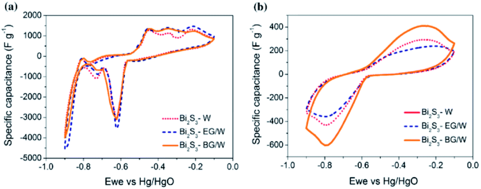 | ||
| Fig. 22 CV curves of Bi2S3 electrodes at (a) 1 mV s−1 and (b) 100 mV s−1.59 | ||
As illustrated in the above cyclic voltammograms, the Bi2S3 electrode materials were tested in a wide potential range from −0.1 to −0.9 V. The distinct redox peaks ascribed in Fig. 22a at −0.6 and −0.45 V during the anodic and cathodic sweeps represent the pseudocapacitive behavior of Bi2S3, respectively. The redox couple can arise from the change in the bismuth valence state (Bi3+/Bi0) or be induced by the frequently reported reversible reaction between Bi2S3 and the OH− ions in the electrolyte.61,120 The other redox couple observed in Fig. 22b could be related to the adsorption–desorption of hydrogen in Bi2S3.121 However, when the scan rate increases to 100 mV s−1, many redox peaks fade, as shown in Fig. 22b. The calculated specific capacitances of Bi2S3–W, Bi2S3–EG/W, and Bi2S3–BG/W from the CV curves, recorded at the scan rate of 1 mV s−1, are found to be 608, 630, and 615 F g−1, respectively. Further, Bi2S3–BG/W showed a specific capacitance of 168 F g−1 at 100 mV s−1 scan rate, which demonstrated its superior capability compared to that of Bi2S3–W (106 F g−1) and Bi2S3-EG/W (118 F g−1).59
Vadivel et al. employed the wet chemical method to synthesize the pure Bi2S3 and Bi2S3–graphene (BG) electrode materials. Fig. 23a shows the CV curves of the BG composite and pure Bi2S3 at the scan rate of 5 mV s−1 in the potential range from −0.2 to −1.0 V. Further, the anodic and cathodic peaks that appeared in the spectrum are due to the oxidation and reduction of OH− ions and Bi2S3 electrode material, respectively. When the scan rate increased from 5 to 100 mV s−1 for the BG composite, as shown in Fig. 23b, the shape of the CV curve was maintained by representing an excellent performance of the electrode material and subsequently increased the anodic and cathodic processes. Further, the presence of graphene in the BG composite increased the capacitance value due to its higher conductivity compared to that of Bi2S3.62
 | ||
| Fig. 23 CV curves of (a) the BG composite and pure Bi2S3 at 5 mV s−1 and (b) the BG composite at different scan rates.62 | ||
The calculated specific capacitances of Bi2S3 and BG composite materials from the GCD curves are shown in Fig. 24a and b, respectively, and the values of the BG composite are 290, 282, 187, 182, 126, and 110 F g−1 at different current densities. Moreover, these values are higher than those of pure Bi2S3 (191, 140, 108, 107, 80, and 68 F g−1) at similar current densities. The effective incorporation of graphene sheets over Bi2S3 nanorods in the BG composite could be the reason behind the improved rate capability. Further, the increased surface area, higher conductive nature, and flexibility of graphene may have influenced the electrochemical performance of the BG composite material.122–124 Moreover, the rod-like structure of the BG composite could have provided more active sites for the redox process of the active material with greater interfacial contact between the electrode and the electrolyte.125,126
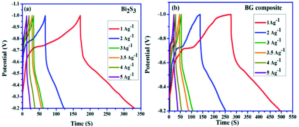 | ||
| Fig. 24 GCD curves of (a) Bi2S3 and (b) BG composite at different current densities.62 | ||
Nie et al.60 prepared X–Bi2S3 (without GO), rGO, and BGNS composites (with GO) using the hydrothermal method. Fig. 25 illustrates the CV and GCD profiles of the above materials. Fig. 25a depicts the typical CV curves of the above products at 5 mV s−1. Further, the CV plots of the BGNS samples expanded along with the decreased additive amounts of GO (BGNS 1, 2, and 3 with 15, 30, and 45 mg of GO, respectively) indicate better capacitance values compared to bare rGO and X–Bi2S3. Specific capacitance values were determined from the GCD curves recorded at the current density of 1 A g−1, as shown in Fig. 25b, for BGNS-3 (201 F g−1), BGNS-2 (342 F g−1) and BGNS-1 (396 F g−1); BGNS-1 exhibited the highest capacitance, which was higher compared to the obtained capacitances for rGO (136 F g−1) and X–Bi2S3 (60 F g−1).
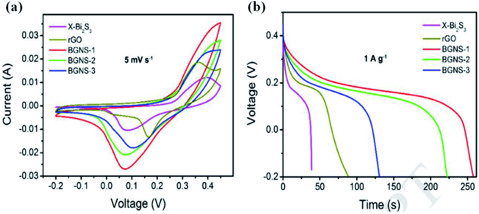 | ||
| Fig. 25 (a) CV curves at a scan rate of 5 mV s−1 and (b) GCD curves at a current density of 1 A g−1.60 | ||
The increased specific capacitance of the BGNS composite may be attributed to the synergistic effect between Bi2S3 and carbon (rGO/GO). It facilitates effective electron transport and faster ion diffusion during the charge–discharge process through the electrolyte when the material employed is an active material for supercapacitor electrodes, thus enforcing the BGNS composite with superior electrochemical performance over bare rGO and pure Bi2S3 nanomaterials. Moreover, the contact area enhances with the decrease in the particle size, which could play a significant role in the accessibility of the composite materials to OH− ions and shorten the ion migration pathway during the charge–discharge process, thus increasing the specific capacitance of the BGNS composite.
5.2. Copper sulfide
Copper sulfide (CuS) has been considered as one of the most promising pseudocapacitor materials due to its excellent metallic properties, high specific capacity, and excellent physical, chemical, structural, and surface properties.127–129 CuS has been synthesized by various methods such as solvothermal method, hydrothermal method, CBD, and CVD. Here, we focus on the solvothermal63,64 and hydrothermal66,69,70 synthesis of CuS only. Huang et al. and Peng et al. used the solvothermal method to synthesize CuS-based electrode materials. The CV curves of CuS–CTAB (cetyltrimethylammonium bromide), CuS–SDBS (sodium dodecylbenzenesulfonate), and pure CuS in the potential range from −0.4 to −0.6 V are shown in Fig. 26a. It can be observed that these CV curves deviate from the ideal rectangular shape, signifying the pseudocapacitive behavior. Fig. 26b represents the GCD profiles of the above electrode materials at a current density of 1 A g−1 and pure CuS shows the highest specific capacitance of 833.3 F g−1 compared to 378.9 F g−1 and 232.4 F g−1 for CuS–CTAB and CuS–SDBS, respectively. As illustrated by the CV and GCD curves, the CuS electrode possesses higher capacitance than CuS–CTAB and CuS–SDBS electrodes due to the thinner layer of CuS. This thinner layer enables the easier penetration of electrolytes to promote electron and charge transfer.63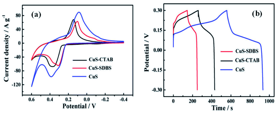 | ||
| Fig. 26 (a) CV and (b) GCD curves of CuS–CTAB, CuS–SDBS, and CuS electrodes.63 | ||
Fig. 27a1 shows the CV curves of solvothermally synthesized CuS, PPy, and CuS@PPy composite at the scan rate of 25 mV s−1 with the electrolyte of 1 M KCl. The insertion and expulsion of K+ ions are indicated in the CV curve of PPy, which possesses a couple of redox peaks.126 The CuS electrode presents a pair of redox peaks at about 0.31 and 0.1 V, which are attributed to the CuS/Cu2S redox transition.127 Similarly, the CuS@PPy composite shows another pair of redox peaks at about 0.31 V and 0.05 V. Fig. 27b gives the GCD curves of CuS, PPy, and CuS@PPy composite electrodes with the capacitance values of 212, 275, and 427 F g−1, respectively, at 1 A g−1. Besides, the increase in the CuS content in the CuS@PPy composite resulted in an increase in the specific capacitance. Further, the specific capacitance of the CuS@PPy composite is higher compared to both pure CuS and PPy. This is probably due to the presence of CuS, which possesses better conductivity than PPy and also provides a path for the insertion and extraction of K+ ions within PPy.60
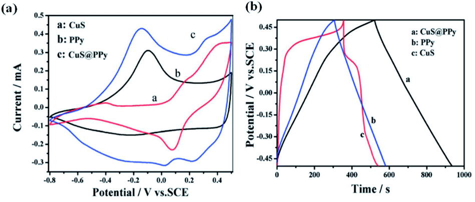 | ||
| Fig. 27 (a) CV curves and (b) GCD curves of CuS, PPy, and CuS@PPy composite.60 | ||
In another study reported by Zhang et al.,65 the specific capacitance values of CuS microspheres were found to be 237, 216, 204, 195, 187, and 180 F g−1 at different current densities. Further, about 75.9% of the original specific capacitance was retained when the current density increased from 0.5 to 8.0 A g−1. Furthermore, the thin CuS nanosheets significantly shorten the diffusion pathway compared to the thick plate-like structure of CuS. Moreover, CuS nanosheets facilitate higher surface area, which increases the rate of redox reaction due to the presence of a large number of electrochemically active sites.
Huang et al.,66 Marimuthu et al.,69 Zhang et al.,68 and Zhai et al.70 reported the electrochemical performance of hydrothermally synthesized CuS. As shown in Fig. 28a, the shape of the CV curves clearly exhibits the pseudocapacitive behavior of CuS/MWCNTs, pure CuS, and pure MWCNTs in the potential range from −0.4 to 0.6 V at the scan rate of 50 mV s−1. It is obvious that the CuS/MWCNTs composite electrode possesses higher capacitance than pure electrodes. Fig. 28b shows the GCD curves of CuS, MWCNTs, and CuS–MWCNTs with the specific capacitance values of 925.1, 555.6, and 2831.0 F g−1, respectively, at a current density of 1 A g−1 in 6.0 M KOH electrolyte. This indicates that the specific capacitance of the hybrid material is greatly enhanced due to the interaction between CuS sheets and WMCNTs, which accelerates electrochemical performance as a result of the effective and rapid conduct of charge carriers.66
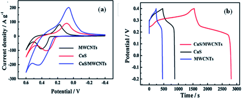 | ||
| Fig. 28 (a) CV curves at 50 mV s−1 and (b) GCD curves at current density of 1 A g−1 of CuS, MWCNTs, and CuS/MWCNTs composite.66 | ||
Zhang et al. reported that the Ni foam-supported CuS nanowall arrays electrode delivers high specific capacitances of 1124, 1053, 912.5, 864.3, 815.5, and 689.4 F g−1 at current densities of 15, 20, 30, 40, 50, and 80 mA cm−2, respectively.68 In another study, the highest specific capacitance of 298 F g−1 at 2 A g−1 current density was obtained for CuS nanoparticles prepared with 1:2 ratio of copper acetate and thiourea.67 However, the hydrolysis of ions and growth of CuS nanoparticles are hindered by the addition of CTAB that induces earlier micellization, which results in the formation of charged micelles on copper sulfide nanoparticles. Moreover, the liberation rate of S2− ions from thiourea has also been influenced by changing the concentration of thiourea in the alkaline precursor solution. The combined effect of thiourea concentration and diverse rate of hydrolysis is positive for assembly and anisotropic growth. The concentration of thiourea greatly affects the physical and electrochemical features of CuS.
In another study, the calculated specific capacitance values of sandwich-type flower-like CuS/carbonized cloth (CSCC) electrodes, prepared at different reaction times such as 3, 4, 5, and 6 h, were found to be 2168, 3468, 3112, and 2876 F cm−2, respectively, at 4 mA cm−2, which were higher than the CC electrode with 61 F cm−2 at the same current density.70
5.3. Nickel sulfide
Nickel sulfide belongs to VI–VIII compound semiconductor and has attracted significant attention owing to its high electronic conductivity, low cost, ease of synthesis, low toxicity, and high specific capacitance.130–132 As widely reported, hydrothermal, chemical bath deposition, wet chemical synthesis, and microwave-assisted synthetic methods have been used to synthesize various micro/nanostructures of nickel sulfide electrode materials. Many different phases of nickel sulfide such as NiS, Ni3S2, NiS2, Ni3S4, Ni7S6, and Ni9S8 have been extensively investigated in recent decades due to their versatile applications in supercapacitors, catalytic hydrogenation, dye-sensitized solar cells, and lithium-ion batteries.Xiong et al.106 studied the CV of Ni3S2 nanorod arrays obtained at various temperatures. The CV curves shown in Fig. 29a exhibit a notable pair of redox peaks in the potential range from −0.2 to 0.7 V. The redox peaks near 0.48 and 0.12 V (vs. Ag/AgCl) can be attributed to the reversible redox reactions of Ni2+/Ni3+. The specific capacitances of three types of Ni3S2 synthesized at different temperatures of 115 °C, 140 °C, and 160 °C at 30 mV s−1 were found to be 420, 464, and 306 F g−1, respectively. The properties of interfacial surface structure and ionic/electronic diffusion of the electrode materials have vital roles in improving the specific capacitance of the supercapacitors. The specific capacitances calculated from the GCD curves shown in Fig. 29b revealed the highest specific capacitance of 694 F g−1 at a discharge current density of 20 mA cm−2 for Ni3S2 nanosheet@nanorods, which was formed at 115 °C. Here, the Ni3S2 nanorods are well wrapped by Ni3S2 nanosheets and possess a highly open structure that offers sufficient space for buffering the volume changes during the charge–discharge process. At the same time, Ni3S2 nanosheets largely increase the contact area between the electrolyte and active materials, and greatly facilitate ion and electron diffusion.
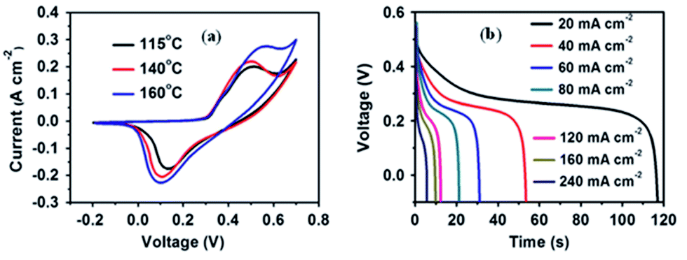 | ||
| Fig. 29 (a) CV curves of Ni3S2 at different temperatures and (b) GCD curves of Ni3S2 at different current densities.106 | ||
The hydrothermally synthesized 3D hierarchical nanostructures of Ni3S2 on Ni foam were studied as a supercapacitor electrode.133 These 3D nanostructures exhibit a significant increase in the active material availability for electrochemical performance. The 3D hierarchical nanostructures of Ni3S2 showed a high specific capacitance of 710.4 F g−1 at the current density of 2 A g−1. Later, Huo et al. prepared the 3D Ni3S2 nanosheets array on Ni foam electrode, which exhibited a high specific capacitance of 1370.4 F g−1 at the current density of 2 A g−1. The good performance of Ni3S2 nanosheets can be ascribed to the unique porous and open structure of the Ni3S2 nanosheets that facilitate the penetration of the electrolyte into the inner part and shorten the ionic diffusion path, hence improving the dynamic performance. Moreover, the open space within the Ni3S2 nanosheets can store a large number of ions, which ensures that sufficient faradaic reactions can take place for energy storage.133
From the CV measurements of pristine NiS and NiS/C-dots composite carried out in 2 M KOH electrolyte solution, it can be seen that both materials exhibit pseudocapacitive nature with the appearance of an oxidation peak and a corresponding reduction peak in their CV profiles. The NiS/C-dots composite material possesses significantly high current density compared to the pristine NiS due to the better charge transport property of the composite material compared to the pristine NiS material (larger peak separation of 0.29 V was observed for pristine NiS). The maximum specific capacitance of 650 F g−1 was obtained for the NiS/C-dots composite, which is larger than that of pristine NiS (480 F g−1) at 10 mV s−1 scan rate. The transport of charge deep inside the matrix is quite fast in NiS/C-dots composite electrode material due to the incorporation of highly conducting carbon dots; therefore, the specific capacitance of the said material is improved.109
Wei et al. performed CV measurements on hollow α-NiS and β-NiS materials in 3.0 M KOH electrolyte by varying the scan rates from 5 to 100 mV s−1. The shape of these curves indicates the pseudocapacitive behavior. The specific capacitances derived from the GCD curves are 562.3 and 501.5 F g−1 for α-NiS and β-NiS, respectively, at 0.6 A g−1. At a higher current density of 6.0 A g−1, the specific capacitance of α-NiS remained at 201.9 F g−1, while that of β-NiS hollow sphere electrode reduced to 169.1 F g−1. Hence, α-NiS hollow sphere electrode is significantly better than the β-NiS electrode in terms of the specific capacitance.110
Shu-Wei Chou and Jeng-Yu synthesized flaky nickel sulfide (Ni3S2) nanostructure on Ni foam by the ED method, which showed a high specific capacitance of 717 F g−1 at 2 A g−1 in 1 M KOH electrolyte solution. The CV shape of the Ni3S2 flaky electrode differs from the rectangular CV shape of an ideal electric double-layer capacitor and reveals diverse pseudocapacitive characteristics.112 Further, a nickel sulfide/electrochemically reduced graphene oxide (erGO) nanocomposite prepared by the ED method has been reported by Liu et al. The CV of this nanocomposite displays distinct pseudocapacitive characteristics, which is quite different from the rectangular CV shape of the erGO-based supercapacitor. This suggests that the total capacitance mainly depends on the nickel sulfide rather than erGO. When compared with sole nickel sulfides,134 the nickel sulfide/erGO nanocomposite shows a higher specific capacitance of 1392.2 F g−1 at a current density of 2 A g−1.113
Pang et al. synthesized NiS2 nanocubes, nanospheres, and nanoparticles by microwave-assisted synthesis. The CV curve of NiS2 nanocubes electrode in 3.0 M KOH electrolyte solution shows a broad redox peak due to the faradaic reactions of NiS2 nanocubes based on the surface redox mechanism of Ni2+ to Ni3+ at the surface. Further, NiS2 nanocube electrodes possess a larger specific capacitance of 695 F g−1 at a current density of 1.25 A g−1 than that of NiS2 nanospheres and nanoparticles.115
5.4. Molybdenum sulfide
Molybdenum disulfide (MoS2) is one of the most considered van der Waals solids, which has unique physical properties when it is in single-layer, multi-layer, or re-stacked layer forms. These can be fabricated by chemical exfoliation from its layered 3D structure.104,135 In particular, the layered structure and inherent conductivity of MoS2 have provoked interest among other transition metal sulfides. Therefore, it is considered to be a suitable replacement for graphene and carbon nanotubes in energy storage applications. Besides, Mo-based substances (such as MoO3, MoO2, and MoS2) make them viable candidates for electrochemical applications due to their various valence states and rich chemical properties.136,137 Further, MoS2 possesses unique atomic and electronic structure.100 Moreover, MoS2 have fourteen different polymorphs with varying electrical and optical properties of interest. A recent simulation-based research shows that the seven out of fourteen polymorphs are both dynamically and mechanically stable, which make them interesting candidates for optoelectronic applications.138 MoS2 continues to attract much attention, particularly in supercapacitors due to its higher intrinsic fast ionic conductivity (than oxides) and higher capacity (than graphite).139–142Hu et al., Balasingam et al., Kanaujiya et al., and Luo et al. synthesized MoS2 nanostructures as electrodes for capacitor applications. Hu et al. synthesized porous tubular C/MoS2 nanocomposite on Ni foam by the hydrothermal method. The CV curve of the nanocomposite electrode exhibits a remarkable reversible redox peak, which suggests the pseudocapacitive properties of the nanocomposite. The GCD parameters display the specific capacitance of 210 F g−1 at the current density of 1 A g−1 for the C/MoS2 nanocomposite, which is higher than that of pure CNTs.96 The double-layer capacitive performance of the MoS2 nanostructures in 1.0 M Na2SO4 electrolyte solution with the potential window of −0.8 to 0.2 V at the scanning rate of 10 mV s−1 was reported by Huang et al., as shown in Fig. 30a. The GCD curve of the MoS2 nanosheets electrode is shown in Fig. 30b with the highest specific capacitance of 129.2 F g−1 at a current density of 1.0 A g−1.97 Further, the specific capacitances of 90.1, 225, and 218.4 F g−1 at the current density of 1 A g−1 have been reported for sponge-like MoS2, flower-like mesoporous MoS2, and irregular MoS2 nanosheet, respectively.101–103
 | ||
| Fig. 30 (a) CV curve and (b) GCD curve of MoS2 nanosheets.97 | ||
Wang et al. synthesized 3D flower-like MoS2 electrode materials through the hydrothermal method by varying the duration of treatment in the autoclave. The calculated specific capacitances revealed that the MoS2-16 electrode (treatment time 16 h) had a higher specific capacitance of 518.7 F g−1 at a current density of 1 A g−1 than those of MoS2-8 (treatment time 8 h) and MoS2-24 (treatment time 24 h) electrodes. This higher specific capacitance of the 3D flower-like MoS2-16 is partially attributed to its ultrathin and porous features, which can facilitate richer electroactive sites and more efficient electron transport.99 Moreover, Yu et al. synthesized MoS2 nanosheets on TiN nanorods (TMS). The CV parameters of the above material revealed that even though TiN significantly contributed to the capacitance, the major contributor was MoS2. The maximum specific capacitance of the TMS-6 electrode (reaction time 6 h) resulted in about 662.2 mF cm−2 at the current density of 1 mA cm−2. It was 4.5 times and 4.9 times higher than that of the pristine MoS2 electrode and TiN electrode, respectively. This is a clear evidence for the presence of synergistic effect in the MoS2–TiN composite.100
Yang et al. synthesized edge-oriented MoS2 thin-film by electrodeposition method and its measured cyclic voltammogram shows quasi-rectangular shapes with a pair of small humps due to the cation intercalation and reversible redox reactions between the valence states of Mo4+ and Mo3+. The specific capacitance of edge-oriented MoS2 thin film is 12.5 mF cm−2 at the scan rate of 50 mV s−1.104
5.5. Tin sulfide
Tin (Sn)-formulated sulfides, such as tin monosulfide (SnS) and tin disulfide (SnS2), may be designated as multifunctional materials due to their potential applications.143 In the compound semiconductors, the IV–VI group binary compound SnS and SnS2 has received much attention as a potential candidate due to its remarkable stability, optical properties, and structural characteristics.144–149 Further, SnS is increasingly being investigated as a photoconverter because it is neither toxic nor expensive, and its commercial availability.150–152 Furthermore, it is a layered semiconductor and possesses an orthorhombic crystal structure. Besides, SnS2 possesses a layered structure, similar to CdI2, in which the tin atoms are located between two hexagonally close-packed sulfur slabs to form a three-atom sandwich structure.153–160Patil et al. deposited the SnS thin films by chemical bath deposition at different deposition times of 120, 240, and 360 min denoted as TS1, TS2, and TS3, respectively. The CV measurements were carried out in a 2 M KOH electrolyte solution for bare SS substrate (stainless steel), TS1, TS2, and TS3 electrodes with a potential range of −0.5 to −1.2 V. The rectangular-shaped CV curves with small redox peaks show that the charge storage is due to redox reactions as well as EDLC-type reactions. The specific capacitance values of TS1, TS2, and TS3 electrodes are found to be 950, 1203, and 1055 F g−1, respectively, at a scan rate of 5 mV s−1. The measured specific capacitance values varied due to the variation in the morphologies of the SnS films at different deposition times. The nanoflower-like morphology of SnS offers a more specific surface area for fast charge intercalation/de-intercalation reactions.95
Moreover, a leaf-like SnS2 nanosheet was synthesized using hydrothermal method by Ma et al. Fig. 31a shows the CV curves of bare nickel foam, bare SnS2 nanosheets, and m-SnS2 hierarchical architectures in the potential range from −0.1 to 0.4 V at the scan rate of 10 mV s−1 in KOH solution. The CV curves of all the electrodes confirm that they are distinct from the ideal rectangular curve originating from the electric double-layer capacitor.3,161 All the electrodes with redox peaks indicate the reversibility of the redox processes, which results from the intercalation of K+ ions into the S–Mo–S layer.162,163 Moreover, it can be seen that the m-SnS2 electrode possesses a higher specific capacitance than that of the bare SnS2 electrode and nickel foam. The GCD curves of bare SnS2 nanosheets and m-SnS2 architectures are shown in Fig. 31b and c, respectively. The specific capacitance values of bare SnS2 and m-SnS2 at a current density of 1 A g−1 are calculated to be 89.4 and 213.2 F g−1, respectively.93
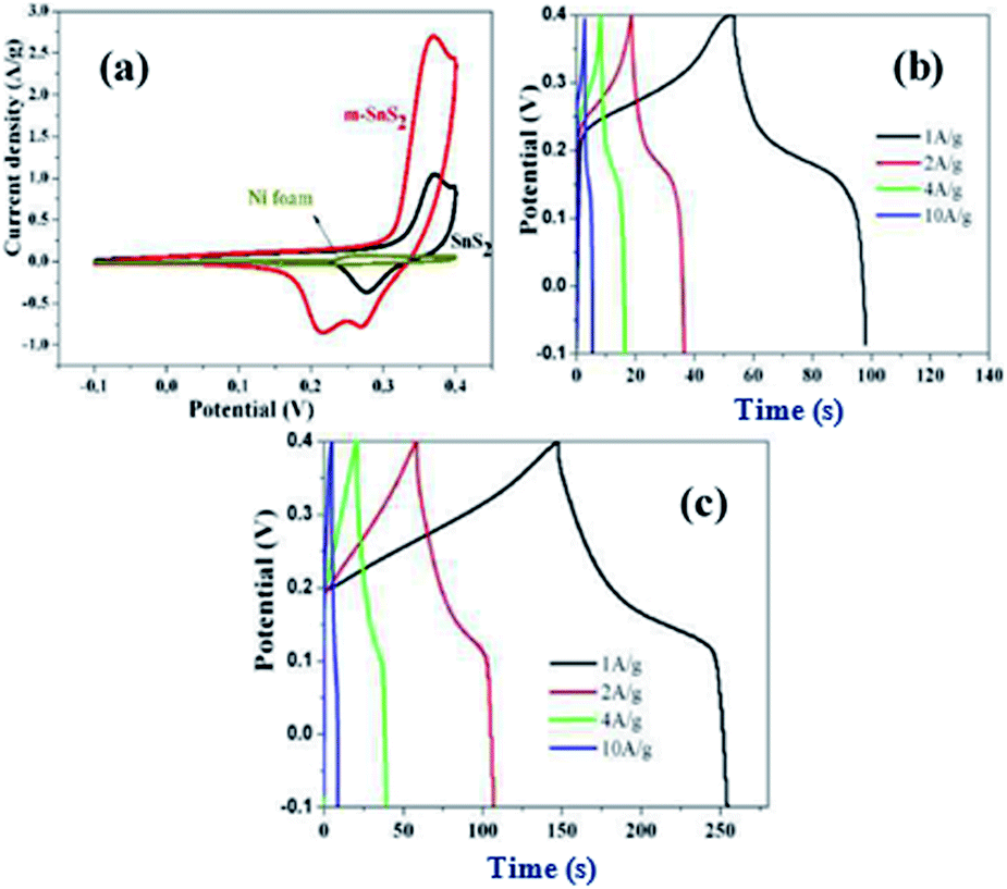 | ||
| Fig. 31 (a) CV curves of bare nickel foam, bare SnS2 nanosheets, and m-SnS2 architectures, and GCD curves of (b) bare SnS2 nanosheets and (c) m-SnS2 architectures.93 | ||
5.6. Cobalt sulfide
Cobalt sulfide is an important member of TMS and a potential candidate for energy storage applications.164 It possesses potential supercapacitor applications due to its several advantages such as low cost, electrical activity, long-term stability, as well as excellent electronic and physicochemical properties.165–168 Further, it possesses a variety of phases such as CoS, CoS2, Co2S3, Co3S4, Co9S8, and Co1−xS, which depends on the ratio of cobalt to sulfur.169 The electrochemical performance is enriched by the high redox activity of cobalt sulfide.170,171 CoS has received special attention due to its rich redox couples (Co2+/Co3+ and Co3+/Co4+), different morphologies, and ultra-high capacitance value.172Several methods, such as solvothermal, CBD, ED, MWA, hot injection, and hydrothermal methods, have been used to synthesize cobalt sulfide nanostructures with a variety of phases. Li et al. have developed an ultralong CoS1.097 nanotube network assembled by interlaced nanoflakes using a simple one-step solvothermal method. Two pairs of redox peaks were observed in the CV curve of CoS1.097 in 2 M aqueous KOH electrolyte, indicating the coexistence of an electric double-layer capacitance and pseudocapacitive behavior. The specific capacitance values of CoS1.097, calculated from the corresponding GCD curves, were found to be approximately 764, 686, 597, 400, and 237 F g−1 at the current densities of 0.5, 1, 2, 5, and 10 A g−1 respectively. Besides, Li et al. prepared 3D flower-like Co1−xS by varying the amount of the precursor of the sulfur source and its CV curve illustrates the faradaic behavior of the Co1−xS electrode material, which contributes to the electron transfer process of the Co2+/Co3+ redox couple. The specific capacitances of the two flower-like structures of Co1−xS, synthesized in diethanolamine (DEA) and calculated from their discharge curves, are 674 and 600 F g−1, respectively. These values are higher than that of the nanospheres of CoS2 (360 F g−1) synthesized in pure water at a current density of 3 A g−1.72
Peng et al. prepared CoS2 hollow sphere electrodes that exhibit high pseudocapacitances of 1301, 1073, 883, 650, and 450 F g−1 at current densities of 1, 2.5, 5, 10, and 20 A g−1, respectively. The highest specific capacitance of hollow sphere CoS2 sample was further confirmed by carrying out comparative studies with bulk CoS2 and other CoS2 spheres (double-shell and yolk–shell). The ultrathin nanosheets build mesoporous spheres that facilitate high surface area and several electroactive sites for redox reaction, which encourage the pseudocapacitive performance of the CoS2 hollow sphere.82,172 Furthermore, Tang et al.74 synthesized CoS2–rGO nanocomposite and its CV measurements were taken in 6 M KOH electrolyte solution. The CV curves shown in Fig. 32a and b reveal the typical pseudocapacitive behavior of the CoS2 and CoS2–rGO electrodes. The CoS2–rGO nanocomposite exhibits a specific capacitance value of 265 F g−1, which is higher than that of CoS2 (135 F g−1). This could be attributed to the synergistic effect of CoS2 and reduced graphene oxide, and the good conductivity of CoS2 nanoparticles might have prevented the agglomeration of CoS2.
 | ||
| Fig. 32 CV curves of (a) CoS2 and (b) CoS2–rGO in 6 M KOH electrolyte.74 | ||
The preparation of CoS nanostructures on nickel foam by the CBD method has been reported by Anil Kumar et al. CV measurements of these nanostructures were carried out in 1 M KOH electrolyte with a potential window between 0.4 and 0.6 V at the scan rate of 30 mV s−1. The CV curve of the ethanol-based CoS electrode showed a pair of well-defined redox peaks as a result of the reversible faradaic reaction. The pseudocapacitance behavior of this electrode was higher when compared to water-based and water/ethanol-based CoS electrodes owing to the resultant large pore size, reduced surface area, and poor adhesion to the substrate.169,173,174 Further, the use of water and water/ethanol system led to less interaction between the KOH electrolyte and the electrode.51,175 The specific capacitances of 31.66, 41.36, and 21.7 F g−1 at the current density of 1.5 A g−1 were observed for the CoS electrodes prepared using water, ethanol, and water/ethanol system, respectively.50
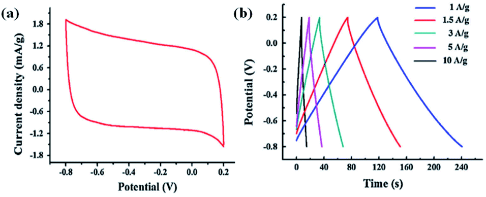
Gervas et al. demonstrated the GCD non-linear curves of CoS-1 (200 °C) and CoS-2 (260 °C), which were synthesized by the hot injection method. It shows typical pseudocapacitance behavior attributed to faradaic redox reactions at the CoS sample surface. A larger charge storage capacity was obtained by the longer charge and discharge time for CoS-2 than CoS-1 at the same current density. The maximum specific capacitances for CoS-2 samples were found to be 440 and 1059 F g−1 as calculated from the GCD (current density of 1 A g−1) and CV (scan rate of 1 mV s−1) curves, respectively. From these results, it was concluded that cobalt sulfide with a lower deficiency of sulfur might be better for electrochemical applications.90
5.7. Quantitative electrochemical performance
In this comprehensive review, the electrochemical energy storage ability of several transition and post-transition metal sulfides along with their usage as electrode materials in supercapacitors and pseudocapacitors have been discussed. The best quantitative electrochemical performance of each transition and post-transition metal sulfide electrode material is summarized in Table 2.| Material | Method of synthesis | Specific capacitance | Conditions | Ref. |
|---|---|---|---|---|
| Bi2S3 | ST | 632.0 F g−1 | Current density of 0.5 A g−1 | 59 |
| Bi2S3–rGO | HT | 396.0 F g−1 | Current density of 1 A g−1 | 60 |
| CuS | ST | 833.3 F g−1 | Current density of 1 A g−1 | 63 |
| CuS/MWCNT/Ni foam | HT | 2831.0 F g−1 | Current density of 1 A g−1 | 66 |
| CuS/Ni foam | HT | 1124.0 F g−1 | Current density of 15 A g−1 | 68 |
| CuS/FTO thin films | HT | 8.3 mF cm−2 | Current density of 1 mA cm−2 | 69 |
| CuS/CCs | HT | 1025.0 mF cm−2 | Current density of 2 mA cm−2 | 70 |
| Co1−xS | ST | 674.0 F g−1 | Current density of 3 A g−1 | 71 |
| CoS1.097 | ST | 686.0 F g−1 | Current density of 1 A g−1 | 72 |
| CoS2 | ST | 1301.0 F g−1 | Current density of 1 A g−1 | 73 |
| CoS2–rGO | ST | 331.0 F g−1 | Current density of 0.5 A g−1 | 74 |
| CoS | ST | 156.0 F g−1 | Current density of 1 A g−1 | 88 |
| CoS2 | HT | 499.0 F g−1 | Current density of 1 A g−1 | 75 |
| rGONF/CoS2 | HT | 635.8 F g−1 | Current density of 1 A g−1 | 76 |
| CCs/CoS2 | HT | 322.0 F g−1 | Current density of 0.5 A g−1 | 77 and 78 |
| 245.0 F g−1 | Current density of 1 A g−1 | |||
| CoS2/MWCNT | HT | 1846.0 F g−1 | Current density of 1 A g−1 | 79 |
| Co9S8/3DG | HT | 1366.0 F g−1 | Current density of 1 A g−1 | 80 |
| Activated Co9S8/3DG | 2317.0 F g−1 | Current density of 1 A g−1 | ||
| Co3S4/rGO | HT | 2314.0 F g−1 | Scan rate of 2 mV s−1 | 81 |
| Co3S4/NF | HT | 2415.0 F g−1 | Current density of 1 A g−1 | 82 |
| CoS | HT | 285.0 F g−1 | Current density of 0.5 A g−1 | 83 |
| 245.0 F g−1 | Current density of 1 A g−1 | |||
| CoS | 932.0 F g−1 | Current density of 5 A g−1 | 84 | |
| CoS/NF | ED | 1471.0 F g−1 | Current density of 4 A g−1 | 85 |
| CoS/eRG/Ni foam | ED | 3785.0 F g−1 | Current density of 1 A g−1 | 86 |
| CoS/NF | CBD | 41.3 F g−1 | Current density of 1.5 A g−1 | 50 |
| CoS/NF | MWA | 586.0 F g−1 | Current density of 1 A g−1 | 87 |
| CoS | MWA | 224.0 F g−1 | Current density of 1 A g−1 | 88 |
| CoSx | Wet chemical synthesis | 475.0 F g−1 | Current density of 5 mA cm−2 | 89 |
| CoS | Hot injection method | 440.0 F g−1 | Current density of 1 A g−1 | 90 |
| CdS/Ni foam | HT | 909.0 F g−1 | Current density of 0.6 A g−1 | 91 |
| γ-MnS/rGO/carbon paper | HT | 547.6 F g−1 | Current density of 1 A g−1 | 92 |
| m-SnS2 | HT | 213.2 F g−1 | Current density of 1 A g−1 | 93 |
| O-SnS | CBD | 1101.0 F g−1 | Current density of 1 mA cm−2 | 94 and 95 |
| C/MoS2 | HT | 210.0 F g−1 | Current density of 1 A g−1 | 96 |
| MoS2 | HT | 129.2 F g−1 | Current density of 1 A g−1 | 97 |
| MoS2 | HT | 92.5 F g−1 | Current density of 0.5 mA cm−2 | 98 |
| MoS2 | HT | 518.7 F g−1 | Current density of 1 A g−1 | 99 |
| MoS2 film | HT | 218.4 F g−1 | Current density of 1 A g−1 | 103 |
| MoS2/Mo foil | ED followed by CVD | 14.5 mF cm−2 | Current density of 1 mA cm−2 | 104 |
| Ni3S2 | HT | 1370.4 F g−1 | Current density of 2 A g−1 | 105 |
| Ni3S2/NF | HT | 694.0 F g−1 | Current density of 20 mA cm−2 | 106 |
| Ni3S2/NF | HT | 710.4 F g−1 | Current density of 2 A g−1 | 107 |
| CNT@Ni3S2 | HT | 514.0 F g−1 | Current density of 4 A g−1 | 108 |
| NiS/C-dot | HT | 880.0 F g−1 | Current density of 2 A g−1 | 109 |
| α-NiS | HT | 562.3 F g−1 | Current density of 0.6 A g−1 | 110 |
| β-NiS | HT | 501.5 F g−1 | Current density of 0.6 A g−1 | 110 |
| NiS/Ni foam | HT | 2384.0 F g−1 | Current density of 1 A g−1 | 111 |
| Ni3S2/NF | ED | 717.0 F g−1 | Current density of 2 A g−1 | 112 |
| Nickel sulfide/ERGO | ED | 1392.2 F g−1 | Current density of 2 A g−1 | 113 |
| NiS/Ti foil | CBD | 788.0 F g−1 | Current density of 1 mA cm−2 | 114 |
| NiS2/NF | MWA | 695.0 F g−1 | Current density of 1.25 A g−1 | 115 |
Here, recent studies reported on transition and post-transition metal sulfide-based capacitors were reviewed. Different structural characteristics and the capacitive nature of particular transition and post-transition metal sulfides, which are widely used in this area, such as Bi2S3, CuS, MoS2, NiS2, NiS, Ni3S2, CoS, CoS2, SnS, and SnS2 have been focused. The controlled morphologies, ability for the formation of different phases, high symmetry in their crystal forms, and enhanced electrical conductivity of the above materials have highly attracted the researchers to expand the applications of these materials. Even though significant advancement has been made in this promising research field, an intensive study is crucial to produce commercially viable applications. In this regard, various transition and post-transition metal sulfides with nanostructured morphologies and increased active surface have been produced by facile synthetic methods in the past decade, which exhibited enhanced capacitance via the improved rate of electron transfer and higher penetration of the electrolyte. Herein, we have discussed the individual electrochemical performance of reviewed transition and post-transition metal sulfides according to the ascending order of the reported highest specific capacitance values.
Nanosheets, sphere-like nanostructures, 3D flower-like microspheres composed of nanosheets, sponge-like nanostructures, and flower-like mesoporous structures of hydrothermally prepared MoS2 were reviewed in this study. Among them, 3D flower-like microspheres composed of nanosheets of MoS2 showed a high specific capacitance of 518.7 F g−1 at a current density of 1 A g−1. Further, autoclaved time and temperature of synthesis played a crucial role in the resultant morphologies of MoS2. Furthermore, in addition to hydrothermal preparation, ED followed by CVD methods of MoS2 preparation was also reported.
Further, γ-MnS/rGO-coated carbon paper showed a specific capacitance of 547.6 F g−1 at a current density of 1 A g−1. An improved electronic conductivity confines aggregation and the lessening of the volume variation of γ-MnS resulted due to the presence of rGO wrapping on γ-MnS nanorods.
The hydrothermally prepared Bi2S3–rGO nanosheet composites with uniform morphology showed a specific capacitance of 396.0 F g−1 at a current density of 1 A g−1, whereas solvothermally prepared sphere-like Bi2S3 nanoparticles showed high specific capacitance of 632.0 F g−1 at a current density of 0.5 A g−1 due to its high specific surface area and facilitated electrochemically active sites for electron flow. Further, a good cycling stability was observed by a capacitance retention of 87% after 500 charge/discharge cycles.
Hydrothermally prepared CdS coated Ni foam resulted a specific capacitance of 909 F g−1 at a current density of 0.6 A g−1. The fabricated supercapacitor showed excellent cycling stability over 5000 charge/discharge cycles at a current density as large as 14.2 A g−1, and 104% of initial capacitance was maintained. However, the toxicity of CdS is of concern to find suitable alternative materials.
Hydrothermally prepared molybdenum-doped leaf-like SnS2 showed higher specific capacitance of 213.2 F g−1 at a current density of 1 A g−1 compared to bare SnS2 electrodes, whereas orthorhombic nanoflower-like SnS prepared by CBD showed a specific capacitance of 1101 F g−1 at a current density of 1 mA cm−2. This could be attributed to nanoflower-like morphology of SnS, which facilitates a higher surface area for fast charge intercalation and de-intercalation reactions. Moreover, these orthorhombic SnS nanoflowers-coated electrodes exhibit good electrochemical stability over 1000 cycles with capacitance retention of 90.2% at 100 mV s−1.
Ni3S2, NiS2 and NiS phases of nickel sulfides are widely focused in this area. Among them, hollow nanoframe-like particles constructed with nanocubes of NiS showed high specific capacitance of 2384 F g−1 at a current density of 1 A g−1 than other phases including 3D nanosheets of Ni3S2, nanoflakes of Ni3S2, hollow spheres of NiS, hierarchical flower-like nanostructure of NiS, and nanocubes and nanospheres of NiS2. The hollow nature of nanoframe-like particles constructed with nanocubes of NiS provides high specific surface area, which facilitates efficient electron transport through good electrical conductivity and promotes electrolyte diffusion between the electrode and the electrolyte. Moreover, capacitance retention of 90.2% after 4000 cycles resulted at a current density of 4 A g−1.
Hydrothermally prepared CuS-based electrode showed high electrochemical performance than solvothermally prepared CuS as hydrothermally prepared CuS coated on Ni form showed a specific capacitance of 1124.0 F g−1 at a current density of 15 A g−1, which is higher compared to CuS coated on CCs. However, the MWCNTs blending with CuS, which was coated on Ni form, showed a high specific capacitance of 2831.0 F g−1 at a current density of 1 A g−1 due to the enhanced specific surface area and excellent conductivity of MWCNTs. Further, MWCNTs facilitate efficient charge transport and promote electrolyte diffusion; thus, the system has good cycling stability over 600 cycles with capacitance retention of more than 90%.
Generally, cobalt sulfide materials lack insufficient support for fast electron transport in faradaic redox reactions at high current density. The high performance of cobalt sulphide electrode was achieved by incorporating electrochemically reduced graphene (eRG). The connected graphene matrix, which is tightly wrapped with CoS, serves as an electronic super path to facilitate fast charge transfer during both charge and discharge processes. Further, this integrated structure led to enlarged electroactive surface area of the electrode materials. CoS/eRG exhibited an impressive high specific capacitance of 3785 F g−1 at a current density of 1 A g−1 with capacitance retention of 82% at 20 A g−1.
6. Summary and perspectives
To produce high-performance supercapacitors with transition and post-transition metal sulfide-based electrodes, a further increase in the specific capacitance can be obtained by investigating the morphology, particle size, surface area, and conductivity of the electrode. Nanostructures of transition and post-transition metal sulfides with high specific surface area can facilitate efficient contact with electrodes and electrolyte ions, providing more electroactive sites for energy storage. For example, various nanostructured materials including 3D flower-like microspheres composed of nanosheets, spheres, nanoflowers, and hollow nanoframes have been reported as high-performance supercapacitor electrode materials. Further, a suitable nanomaterial can be integrated with metal sulfides to overcome the drawbacks of conductivity of individual metal sulfides by providing versatile platforms for efficient charge transfer.Due to their high electrochemical performances, Bi2S3, CuS, MoS2, NiS2, NiS, Ni3S2, CoS, CoS2, CdS, SnS, and SnS2 are effective candidates as electrodes for supercapacitors, which can also be integrated with DSSC in order to build integrated solar/photo capacitors. However, in heterostructured photocapacitors, the capacitive nature is achieved by the oxidation of lower chemical state of sulfide materials into their higher chemical state by forming their oxides in the active photoelectrodes. For this purpose, CoS, NiS, Ni3S2, SnS, PbS, and Bi2S3 are particularly the most potential candidates as active electrodes since their sulfides are in lower oxidation state. However, PbS should be avoided due to its toxicity. In recent times, self-powered photocapacitors have attracted much interest due to their free energy conversion from the sun and self-charging properties; thus, the growth of such photocapacitors may be beneficial to be used along with/or replace batteries in many smart electronic devices in the future. We hope that this comprehensive review on transition and post-transition metal sulfides in supercapacitors will encourage further research into the potential application of the same photocapacitors.
Author contributions
Conceptualization: K. T., D. V., M. S.; methodology: K. T., A. P., D. V., M. S.; formal analysis: K. T., A. P.; software: K. T., A. P.; investigation: K. T., A. P., D. V., M. S.; validation: K. T., A. P., D. V., M. S., P. R.; writing – original draft: K. T., A. P.; visualization: K. T., A. P., D. V., M. S.; writing – review & editing: K. T., A. P., A. Y., Y. S., M. S., D. V., P. R.; supervision: M. S., A. Y., D. V., P. R.; project administration: D. V., P. R.; funding acquisition: D. V., P. R.; all authors have read and agreed to the published version of the manuscript.Conflicts of interest
There are no conflicts to declare.References
- X. Cao, C. Tan, X. Zhang, W. Zhao and H. Zhang, Adv. Mater., 2016, 28, 6167–6196 CrossRef CAS PubMed.
- M. Zhao, Q. Zhao, J. Qiu, H. Xue and H. Pang, RSC Adv., 2016, 6, 95449–95468 RSC.
- D. Yu, Q. Qian, L. Wei, W. Jiang, K. Goh, J. Wei, J. Zhang and Y. Chen, Chem. Soc. Rev., 2015, 44, 647–662 RSC.
- D. Mohler and D. Sowder, in Renewable Energy Integration, Elsevier, 2014, pp. 285–292 Search PubMed.
- A. Pirashanthan, T. Murugathas, K. Mariappan, P. Ravirajan, D. Velauthapillai and S. Yohi, Mater. Lett., 2020, 274, 127997 CrossRef CAS.
- A. Pirashanthan, M. Thanihaichelvan, K. Mariappan, D. Velauthapillai, P. Ravirajan and Y. Shivatharsiny, Sol. Energy, 2021, 225, 399–406 CrossRef CAS.
- T. Rajaramanan, S. Shanmugaratnam, V. Gurunanthanan, S. Yohi, D. Velauthapillai, P. Ravirajan and M. Senthilnanthanan, Catalysts, 2021, 11, 690 CrossRef CAS.
- A. Pirashanthan, D. Velauthapillai, N. Robertson and P. Ravirajan, Sci. Rep., 2021, 11, 1–8 CrossRef PubMed.
- H. Jiang, P. S. Lee and C. Li, Energy Environ. Sci., 2013, 6, 41–53 RSC.
- R. Liu, Y. Liu, H. Zou, T. Song and B. Sun, Nano Res., 2017, 10, 1545–1559 CrossRef CAS.
- M. Yilmaz, S. Hsu, S. Raina, M. Howell and W. P. Kang, J. Renewable Sustainable Energy, 2018, 10, 063503 CrossRef.
- T. M. I. Mahlia, T. J. Saktisahdan, A. Jannifar, M. H. Hasan and H. S. C. Matseelar, Renewable Sustainable Energy Rev., 2014, 33, 532–545 CrossRef.
- D. Li, J. Shi and C. Li, Small, 2018, 14, 1–22 Search PubMed.
- C. Yang, J. Chen, X. Ji, T. P. Pollard, X. Lü, C. J. Sun, S. Hou, Q. Liu, C. Liu, T. Qing, Y. Wang, O. Borodin, Y. Ren, K. Xu and C. Wang, Nature, 2019, 569, 245–250 CrossRef CAS PubMed.
- A. K. Shukla, S. Sampath and K. Vijayamohanan, Curr. Sci., 2000, 79, 1656–1661 CAS.
- C. Liu, Z. G. Neale and G. Cao, Mater. Today, 2016, 19, 109–123 CrossRef CAS.
- M. Lee, Y. Yoo, J. H. Kwak, Y. S. Yun, H. G. Jung, D. Byun, S. H. Oh and H. D. Lim, Chem. Eng. J., 2021, 412, 128549 CrossRef CAS.
- C. M. Costa, J. C. Barbosa, R. Gonçalves, H. Castro, F. J. D. Campo and S. Lanceros-Méndez, Energy Storage Mater., 2021, 37, 433–465 CrossRef.
- L. Zeng, L. Qiu and H. M. Cheng, Energy Storage Mater., 2019, 23, 434–438 CrossRef.
- D. Larcher and J. M. Tarascon, Nat. Chem., 2015, 7, 19–29 CrossRef CAS PubMed.
- P. Breeze, in Power System Energy Storage Technologies, Elsevier, 2018, vol. 106, pp. 61–68 Search PubMed.
- K. K. Kar, Handbook of Nanocomposite Supercapacitor Materials I, Springer International Publishing, Cham, 2020, vol. 300 Search PubMed.
- Y. Zhou, H. Qi, J. Yang, Z. Bo, F. Huang, M. S. Islam, X. Lu, L. Dai, R. Amal, C. H. Wang and Z. Han, Energy Environ. Sci., 2021, 14, 1854–1896 RSC.
- Y. Zhou, Y. Wang, K. Wang, L. Kang, F. Peng, L. Wang and J. Pang, Appl. Energy, 2020, 260, 114169 CrossRef.
- W. Jing, C. H. Lai, W. S. H. Wong and M. L. D. Wong, Appl. Energy, 2018, 224, 340–356 CrossRef.
- J. Chen and P. S. Lee, Adv. Energy Mater., 2021, 11, 2003311 CrossRef CAS.
- M. Bahdanchyk, M. Hashempour and A. Vicenzo, Electrochim. Acta, 2020, 332, 135503 CrossRef CAS.
- N. Wu, Mater. Chem. Phys., 2002, 75, 6–11 CrossRef CAS.
- H. Choi and H. Yoon, Nanomaterials, 2015, 5, 906–936 CrossRef CAS PubMed.
- T. Miyasaka and T. N. Murakami, Appl. Phys. Lett., 2004, 85, 3932–3934 CrossRef CAS.
- T. N. Murakami, N. Kawashima and T. Miyasaka, Chem. Commun., 2005, 3346 RSC.
- M. Gong, A. Kirkeminde, N. Kumar, H. Zhao and S. Ren, Chem. Commun., 2013, 49, 9260 RSC.
- X. Xia, J. Luo, Z. Zeng, C. Guan, Y. Zhang, J. Tu, H. Zhang and H. J. Fan, Sci. Rep., 2012, 2, 1–6 Search PubMed.
- R. Liu, C. Liu and S. Fan, J. Mater. Chem. A, 2017, 5, 23078–23084 RSC.
- A. P. Cohn, W. R. Erwin, K. Share, L. Oakes, A. S. Westover, R. E. Carter, R. Bardhan and C. L. Pint, Nano Lett., 2015, 15, 2727–2731 CrossRef CAS PubMed.
- G. Maddala, M. Ambapuram, V. Tankasala and R. Mitty, ACS Appl. Energy Mater., 2021, 4, 11225–11233 CrossRef CAS.
- P. Chen, C. Cao, C. Ding, Z. Yin, S. Qi, J. Guo, M. Zhang and Z. Sun, J. Power Sources, 2022, 521, 230920 CrossRef CAS.
- M. Wu, X. Zhao, J. Gao, J. Guo, J. Xiao and R. Chen, Surf. Interfaces, 2022, 31, 101983 CrossRef.
- D. Rand, M. Jakešová, G. Lubin, I. Vėbraitė, M. David-Pur, V. Đerek, T. Cramer, N. S. Sariciftci, Y. Hanein and E. D. Głowacki, Adv. Mater., 2018, 30, 1–11 Search PubMed.
- A. S. Dahlan, A. Tataroʇlu, A. A. Al-Ghamdi, A. A. Al-Ghamdi, S. Bin-Omran, Y. Al-Turki, F. El-Tantawy and F. Yakuphanoglu, J. Alloys Compd., 2015, 646, 1151–1156 CrossRef CAS.
- A. Winchester, S. Ghosh, S. Feng, A. L. Elias, T. Mallouk, M. Terrones and S. Talapatra, ACS Appl. Mater. Interfaces, 2014, 6, 2125–2130 CrossRef CAS PubMed.
- S. Ratha and C. S. Rout, ACS Appl. Mater. Interfaces, 2013, 5, 11427–11433 CrossRef CAS PubMed.
- J. Feng, X. Sun, C. Wu, L. Peng, C. Lin, S. Hu, J. Yang and Y. Xie, J. Am. Chem. Soc., 2011, 133, 17832–17838 CrossRef CAS PubMed.
- J. Yun, Y. Noh, C.-H. Lee, S. Na, S. Lee, S. M. Jo, H. Joh and D. Kim, Small, 2014, 10, 2319–2324 CrossRef CAS PubMed.
- J. H. Rhee, C. Chung and E. W. Diau, NPG Asia Mater., 2013, 5, e68 CrossRef CAS.
- S. Shanmugaratnam, B. Selvaratnam, A. Baride, R. Koodali, P. Ravirajan, D. Velauthapillai and Y. Shivatharsiny, Catalysts, 2021, 11, 589 CrossRef CAS.
- Y. Chen, B. Song, X. Tang, L. Lu and J. Xue, Small, 2014, 10, 1536–1543 CrossRef CAS PubMed.
- M. Cabán-Acevedo, M. L. Stone, J. R. Schmidt, J. G. Thomas, Q. Ding, H.-C. Chang, M.-L. Tsai, J.-H. He and S. Jin, Nat. Mater., 2015, 14, 1245–1251 CrossRef PubMed.
- S. Mao, Z. Wen, S. Ci, X. Guo, K. K. Ostrikov and J. Chen, Small, 2015, 11, 414–419 CrossRef CAS PubMed.
- Y. Anil Kumar, S. Srinivasa Rao, D. Punnoose, C. Venkata Tulasivarma, C. V. V. M. Gopi, K. Prabakar and H. Kim, R. Soc. Open Sci., 2017, 4, 170427 CrossRef PubMed.
- Z. Chen, Z. Wan, T. Yang, M. Zhao, X. Lv, H. Wang, X. Ren and X. Mei, Sci. Rep., 2016, 6, 25151 CrossRef CAS PubMed.
- Y. Zhou, D. Yan, H. Xu, J. Feng, X. Jiang, J. Yue, J. Yang and Y. Qian, Nano Energy, 2015, 12, 528–537 CrossRef CAS.
- T. Peng, Z. Qian, J. Wang, D. Song, J. Liu, Q. Liu and P. Wang, J. Mater. Chem. A, 2014, 2, 19376–19382 RSC.
- D. Cai, D. Wang, C. Wang, B. Liu, L. Wang, Y. Liu, Q. Li and T. Wang, Electrochim. Acta, 2015, 151, 35–41 CrossRef CAS.
- H. Jia, Z. Wang, X. Zheng, Y. Cai, J. Lin, H. Liang, J. Qi, J. Cao, J. Feng and W. Fei, Electrochim. Acta, 2019, 312, 54–61 CrossRef CAS.
- S. K. Shinde, M. B. Jalak, S. Y. Kim, H. M. Yadav, G. S. Ghodake, A. A. Kadam and D.-Y. Kim, Ceram. Int., 2018, 44, 23102–23108 CrossRef CAS.
- S. Safshekan, I. Herraiz-Cardona, D. Cardenas-Morcoso, R. Ojani, M. Haro and S. Gimenez, ACS Energy Lett., 2017, 2, 469–475 CrossRef CAS.
- T. Kajana, D. Velauthapillai, Y. Shivatharsiny, P. Ravirajan, A. Yuvapragasam and M. Senthilnanthanan, J. Photochem. Photobiol., A, 2020, 401, 112784 CrossRef CAS.
- E. Miniach and G. Gryglewicz, J. Mater. Sci., 2018, 53, 16511–16523 CrossRef CAS.
- G. Nie, X. Lu, J. Lei, L. Yang and C. Wang, Electrochim. Acta, 2015, 154, 24–30 CrossRef CAS.
- H. Yang, J. Xie and C. M. Li, RSC Adv., 2014, 4, 48666–48670 RSC.
- S. Vadivel, A. N. Naveen, V. P. Kamalakannan, P. Cao and N. Balasubramanian, Appl. Surf. Sci., 2015, 351, 635–645 CrossRef CAS.
- K. Huang, J. Zhang and Y. Fan, J. Alloys Compd., 2015, 625, 158–163 CrossRef CAS.
- H. Peng, G. Ma, K. Sun, J. Mu, H. Wang and Z. Lei, J. Mater. Chem. A, 2014, 2, 3303 RSC.
- J. Zhang, H. Feng, J. Yang, Q. Qin, H. Fan, C. Wei and W. Zheng, ACS Appl. Mater. Interfaces, 2015, 7, 21735–21744 CrossRef CAS PubMed.
- K. Huang, J. Zhang and K. Xing, Electrochim. Acta, 2014, 149, 28–33 CrossRef CAS.
- N. Sonai Muthu, S. D. Samikannu and M. Gopalan, Ionics, 2019, 25, 4409–4423 CrossRef CAS.
- Y. Zhang, J. Xu, Y. Zheng, X. Hu, Y. Shang and Y. Zhang, RSC Adv., 2016, 6, 59976–59983 RSC.
- T. Marimuthu, N. Anandhan, R. Panneerselvam, K. P. Ganesan and A. A. Roselin, Nano-Struct. Nano-Objects, 2019, 17, 138–147 CrossRef.
- S. Zhai, K. Jin, M. Zhou, Z. Fan, H. Zhao, Y. Zhao, X. Li and Z. Cai, Colloids Surf., A, 2019, 575, 75–83 CrossRef CAS.
- Y. Li, S. Liu, W. Chen, S. Li, L. Shi and Y. Zhao, J. Alloys Compd., 2017, 712, 139–146 CrossRef CAS.
- S. Liu, C. Mao, Y. Niu, F. Yi, J. Hou, S. Lu, J. Jiang, M. Xu and C. Li, ACS Appl. Mater. Interfaces, 2015, 7, 25568–25573 CrossRef CAS PubMed.
- S. Peng, L. Li, H. Tan, R. Cai, W. Shi, C. Li, S. G. Mhaisalkar, M. Srinivasan, S. Ramakrishna and Q. Yan, Adv. Funct. Mater., 2014, 24, 2155–2162 CrossRef CAS.
- J. Tang, J. Shen, N. Li and M. Ye, Ceram. Int., 2014, 40, 15411–15419 CrossRef CAS.
- X. Zeng, B. Yang, X. Li and R. Yu, Electrochim. Acta, 2017, 240, 341–349 CrossRef CAS.
- Q. Chen, D. Cai and H. Zhan, J. Alloys Compd., 2017, 706, 126–132 CrossRef CAS.
- R. Ren, M. S. Faber, R. Dziedzic, Z. Wen, S. Jin, S. Mao and J. Chen, Nanotechnology, 2015, 26, 494001 CrossRef PubMed.
- M. S. Faber, R. Dziedzic, M. A. Lukowski, N. S. Kaiser, Q. Ding and S. Jin, J. Am. Chem. Soc., 2014, 136, 10053–10061 CrossRef CAS PubMed.
- A. Sarkar, A. K. Chakraborty, S. Bera and S. Krishnamurthy, J. Phys. Chem. C, 2018, 122, 18237–18246 CrossRef CAS.
- T.-W. Lin, C.-S. Dai, T.-T. Tasi, S.-W. Chou, J.-Y. Lin and H.-H. Shen, Chem. Eng. J., 2015, 279, 241–249 CrossRef CAS.
- S. J. Patil, J. H. Kim and D. W. Lee, J. Power Sources, 2017, 342, 652–665 CrossRef CAS.
- B. Xin, Y. Zhao and C. Xu, J. Solid State Electrochem., 2016, 20, 2197–2205 CrossRef CAS.
- H. Wan, X. Ji, J. Jiang, J. Yu, L. Miao, L. Zhang, S. Bie, H. Chen and Y. Ruan, J. Power Sources, 2013, 243, 396–402 CrossRef CAS.
- Y. Zhao, Z. Shi, T. Lin, L. Suo, C. Wang, J. Luo, Z. Ruan, C. Wang and J. Li, J. Power Sources, 2019, 412, 321–330 CrossRef CAS.
- J.-Y. Lin and S.-W. Chou, RSC Adv., 2013, 3, 2043–2048 RSC.
- J. Shi, X. Li, G. He, L. Zhang and M. Li, J. Mater. Chem. A, 2015, 3, 20619–20626 RSC.
- F. Luo, J. Li, H. Yuan and D. Xiao, Electrochim. Acta, 2014, 123, 183–189 CrossRef CAS.
- B. You, N. Jiang, M. Sheng and Y. Sun, Chem. Commun., 2015, 51, 4252–4255 RSC.
- F. Tao, Y. Zhao, G. Zhang and H. Li, Electrochem. Commun., 2007, 9, 1282–1287 CrossRef CAS.
- C. Gervas, M. D. Khan, S. Mlowe, C. Zhang, C. Zhao, R. K. Gupta, M. P. Akerman, P. Mashazi, T. Nyokong and N. Revaprasadu, ChemElectroChem, 2019, 6, 2560–2569 CrossRef CAS.
- P. Xu, J. Liu, P. Yan, C. Miao, K. Ye, K. Cheng, J. Yin, D. Cao, K. Li and G. Wang, J. Mater. Chem. A, 2016, 4, 4920–4928 RSC.
- G. Zhang, M. Kong, Y. Yao, L. Long, M. Yan, X. Liao, G. Yin, Z. Huang, A. M. Asiri and X. Sun, Nanotechnology, 2017, 28, 065402 CrossRef PubMed.
- L. Ma, L. Xu, X. Zhou, X. Xu and L. Zhang, RSC Adv., 2015, 5, 105862–105868 RSC.
- A. M. Patil, V. C. Lokhande, U. M. Patil, P. A. Shinde and C. D. Lokhande, ACS Sustainable Chem. Eng., 2018, 6, 787–802 CrossRef CAS.
- A. M. Patil, V. C. Lokhande, U. M. Patil, P. A. Shinde and C. D. Lokhande, ACS Sustainable Chem. Eng., 2018, 6, 787–802 CrossRef CAS.
- B. Hu, X. Qin, A. M. Asiri, K. A. Alamry, A. O. Al-Youbi and X. Sun, Electrochim. Acta, 2013, 100, 24–28 CrossRef CAS.
- K. Huang, J. Zhang, G. Shi and Y. Liu, Electrochim. Acta, 2014, 132, 397–403 CrossRef CAS.
- K. Krishnamoorthy and G. Kumar, Mater. Res. Bull., 2014, 50, 499–502 CrossRef CAS.
- F. Wang, G. Li, J. Zheng, J. Ma, C. Yang and Q. Wang, RSC Adv., 2018, 8, 38945–38954 RSC.
- M. Yu, S. Zhao, H. Feng, L. Hu, X. Zhang, Y. Zeng, Y. Tong and X. Lu, ACS Energy Lett., 2017, 2, 1862–1868 CrossRef CAS.
- S. K. Balasingam, M. Lee, B. H. Kim, J. S. Lee and Y. Jun, Dalton Trans., 2017, 46, 2122–2128 RSC.
- N. Kanaujiya, N. Kumar, Y. Sharma and G. D. Varma, J. Electron. Mater., 2019, 48, 904–915 CrossRef CAS.
- S. Luo, L. Xu, J. Li, W. Yang, M. Liu and L. Ma, Nano, 2020, 15, 2050011 CrossRef CAS.
- Y. Yang, H. Fei, G. Ruan, C. Xiang and J. M. Tour, Adv. Mater., 2014, 26, 8163–8168 CrossRef CAS PubMed.
- H. Huo, Y. Zhao and C. Xu, J. Mater. Chem. A, 2014, 2, 15111 RSC.
- X. Xiong, B. Zhao, D. Ding, D. Chen, C. Yang, Y. Lei and M. Liu, NPG Asia Mater., 2016, 8, e300 CrossRef.
- Z. Zhang, Z. Huang, L. Ren, Y. Shen, X. Qi and J. Zhong, Electrochim. Acta, 2014, 149, 316–323 CrossRef CAS.
- T. Zhu, H. B. Wu, Y. Wang, R. Xu and X. W. D. Lou, Adv. Energy Mater., 2012, 2, 1497–1502 CrossRef CAS.
- S. Sahoo, A. K. Satpati, P. K. Sahoo and P. D. Naik, ACS Omega, 2018, 3, 17936–17946 CrossRef CAS PubMed.
- C. Wei, C. Cheng, J. Zhao, Y. Wang, Y. Cheng, Y. Xu, W. Du and H. Pang, Chem.–Asian J., 2015, 10, 679–686 CrossRef CAS PubMed.
- X.-Y. Yu, L. Yu, H. Bin Wu and X. W. D. Lou, Angew. Chem., Int. Ed., 2015, 54, 5331–5335 CrossRef CAS PubMed.
- S. Chou and J. Lin, J. Electrochem. Soc., 2013, 160, D178–D182 CrossRef CAS.
- X. Liu, X. Qi, Z. Zhang, L. Ren, Y. Liu and L. Meng, Ceram. Int., 2014, 40, 8189–8193 CrossRef CAS.
- P. Gaikar, S. P. Pawar, R. S. Mane, M. Nuashad and D. V. Shinde, RSC Adv., 2016, 6, 112589–112593 RSC.
- H. Pang, C. Wei, X. Li, G. Li, Y. Ma, S. Li, J. Chen and J. Zhang, Sci. Rep., 2015, 4, 3577 CrossRef PubMed.
- F. Paquin, J. Rivnay, A. Salleo, N. Stingelin and C. Silva, J. Mater. Chem. C, 2015, 3, 10715–10722 RSC.
- W. Lou, M. Chen, X. Wang and W. Liu, Chem. Mater., 2007, 19, 872–878 CrossRef CAS.
- L. Fang, Y. Qiu, T. Zhai, F. Wang, M. Lan, K. Huang and Q. Jing, Colloids Surf., A, 2017, 535, 41–48 CrossRef CAS.
- W. Zong, F. Lai, G. He, J. Feng, W. Wang, R. Lian, Y.-E. Miao, G.-C. Wang, I. P. Parkin and T. Liu, Small, 2018, 14, 1801562 CrossRef PubMed.
- C. H. Ng, H. N. Lim, S. Hayase, Z. Zainal, S. Shafie and N. M. Huang, Ind. Eng. Chem. Res., 2018, 57, 2146–2154 CrossRef CAS.
- P. Hu, Y. Cao and B. Lu, Mater. Lett., 2013, 106, 297–300 CrossRef CAS.
- J. Yang, X. Duan, W. Guo, D. Li, H. Zhang and W. Zheng, Nano Energy, 2014, 5, 74–81 CrossRef CAS.
- B. Wang, Y. Wang, J. Park, H. Ahn and G. Wang, J. Alloys Compd., 2011, 509, 7778–7783 CrossRef CAS.
- D. H. Nagaraju, Q. Wang, P. Beaujuge and H. N. Alshareef, J. Mater. Chem. A, 2014, 2, 17146–17152 RSC.
- V. D. Nithya, B. Hanitha, S. Surendran, D. Kalpana and R. Kalai Selvan, Ultrason. Sonochem., 2015, 22, 300–310 CrossRef CAS PubMed.
- S. Vijayakumar, S. Nagamuthu and G. Muralidharan, ACS Appl. Mater. Interfaces, 2013, 5, 2188–2196 CrossRef CAS PubMed.
- K. J. Huang, J. Z. Zhang, Y. Liu and Y. M. Liu, Int. J. Hydrogen Energy, 2015, 40, 10158–10167 CrossRef CAS.
- Y. Lu, B. Li, S. Zheng, Y. Xu, H. Xue and H. Pang, Adv. Funct. Mater., 2017, 27, 1–28 Search PubMed.
- U. Shamraiz, R. A. Hussain and A. Badshah, J. Solid State Chem., 2016, 238, 25–40 CrossRef CAS.
- M. Naveed, W. Younas, C. Cao, S. Rafai, S. Khalid, Z. Wang and C. Qiao, ChemNanoMat, 2019, 5, 1216–1224 CrossRef CAS.
- B. Safdar, J. A. Rajesh, S.-H. Kang, H. Kim and K.-S. Ahn, J. Alloys Compd., 2020, 826, 154211 CrossRef CAS.
- S. Suresh, S. S. R. Solay Anand, R. Arul and D. Isha, Chalcogenide Lett., 2016, 13, 291–299 CAS.
- B. Li, M. Zheng, H. Xue and H. Pang, Inorg. Chem. Front., 2016, 3, 175–202 RSC.
- Z. Xing, Q. Chu, X. Ren, J. Tian, A. M. Asiri, K. A. Alamry, A. O. Al-Youbi and X. Sun, Electrochem. Commun., 2013, 32, 9–13 CrossRef CAS.
- X. Hu, W. Zhang, X. Liu, Y. Mei and Y. Huang, Chem. Soc. Rev., 2015, 44, 2376–2404 RSC.
- K. Krishnamoorthy, P. Pazhamalai, G. K. Veerasubramani and S. J. Kim, J. Power Sources, 2016, 321, 112–119 CrossRef CAS.
- T. N. Y. Khawula, K. Raju, P. J. Franklyn, I. Sigalas and K. I. Ozoemena, J. Mater. Chem. A, 2016, 4, 6411–6425 RSC.
- H. Eidsvåg, M. Rasukkannu, D. Velauthapillai and P. Vajeeston, RSC Adv., 2021, 11, 3759–3769 RSC.
- X. Cao, C. Tan, X. Zhang, W. Zhao and H. Zhang, Adv. Mater., 2016, 28, 6167–6196 CrossRef CAS PubMed.
- R. Thangappan, S. Kalaiselvam, A. Elayaperumal, R. Jayavel, M. Arivanandhan, R. Karthikeyan and Y. Hayakawa, Dalton Trans., 2016, 45, 2637–2646 RSC.
- K. Krishnamoorthy, G. K. Veerasubramani, P. Pazhamalai and S. J. Kim, Electrochim. Acta, 2016, 190, 305–312 CrossRef CAS.
- K.-J. Huang, L. Wang, J.-Z. Zhang, L.-L. Wang and Y.-P. Mo, Energy, 2014, 67, 234–240 CrossRef CAS.
- G. Hatui, G. Chandra Nayak, G. Udayabhanu, Y. K. Mishra and D. D. Pathak, New J. Chem., 2017, 41, 2702–2716 RSC.
- A. P. Chowdhury, B. H. Shambharkar, S. G. Ghugal, S. S. Umare and A. G. Shende, RSC Adv., 2016, 6, 108290–108297 RSC.
- L. A. Burton, D. Colombara, R. D. Abellon, F. C. Grozema, L. M. Peter, T. J. Savenije, G. Dennler and A. Walsh, Chem. Mater., 2013, 25, 4908–4916 CrossRef CAS.
- S. H. Chaki, M. D. Chaudhary and M. P. Deshpande, Adv. Nat. Sci.: Nanosci. Nanotechnol., 2014, 5, 045010 CAS.
- S. H. Chaki, M. D. Chaudhary and M. P. Deshpande, J. Semicond., 2016, 37, 053001 CrossRef.
- G. A. Tritsaris, B. D. Malone and E. Kaxiras, J. Appl. Phys., 2014, 115, 173702 CrossRef.
- J. Vidal, S. Lany, J. Francis, R. Kokenyesi and J. Tate, J. Appl. Phys., 2014, 115, 113507 CrossRef.
- A. M. Tripathi and S. Mitra, RSC Adv., 2014, 4, 10358 RSC.
- H. Chauhan, M. K. Singh, S. A. Hashmi and S. Deka, RSC Adv., 2015, 5, 17228–17235 RSC.
- S. Sánchez-Salcedo, A. Nieto and M. Vallet-Regí, Chem. Eng. J., 2008, 137, 62–71 CrossRef.
- H. Chauhan, M. K. Singh, P. Kumar, S. A. Hashmi and S. Deka, Nanotechnology, 2017, 28, 025401 CrossRef PubMed.
- N. Parveen, S. A. Ansari, H. R. Alamri, M. O. Ansari, Z. Khan and M. H. Cho, ACS Omega, 2018, 3, 1581–1588 CrossRef CAS PubMed.
- U. Chalapathi, B. Poornaprakash, B. Purushotham Reddy and S. Park, Thin Solid Films, 2017, 640, 81–87 CrossRef CAS.
- S. H. Chaki, H. J. Joshi, J. P. Tailor and M. P. Deshpande, Mater. Res. Express, 2017, 4, 076402 CrossRef.
- N. Anitha, M. Anitha, J. Raj Mohamed, S. Valanarasu and L. Amalraj, J. Asian Ceram. Soc., 2018, 6, 121–131 CrossRef.
- J.-R. Tu, X.-F. Shi, H.-W. Lu, N.-X. Yang and Y.-J. Yuan, Mater. Lett., 2016, 185, 303–306 CrossRef CAS.
- N. Parveen, S. A. Ansari, H. R. Alamri, M. O. Ansari, Z. Khan and M. H. Cho, ACS Omega, 2018, 3, 1581–1588 CrossRef CAS PubMed.
- L. A. Burton, T. J. Whittles, D. Hesp, W. M. Linhart, J. M. Skelton, B. Hou, R. F. Webster, G. O'Dowd, C. Reece, D. Cherns, D. J. Fermin, T. D. Veal, V. R. Dhanak and A. Walsh, J. Mater. Chem. A, 2016, 4, 1312–1318 RSC.
- Y. Wang and Y. Xia, Adv. Mater., 2013, 25, 5336–5342 CrossRef CAS PubMed.
- K. Gopalakrishnan, S. Sultan, A. Govindaraj and C. N. R. Rao, Nano Energy, 2015, 12, 52–58 CrossRef CAS.
- M. Acerce, D. Voiry and M. Chhowalla, Nat. Nanotechnol., 2015, 10, 313–318 CrossRef CAS PubMed.
- Q. Chen, H. Li, C. Cai, S. Yang, K. Huang, X. Wei and J. Zhong, RSC Adv., 2013, 3, 22922 RSC.
- S. Chen, H. Chen, M. Fan, C. Li and K. Shu, J. Sol-Gel Sci. Technol., 2016, 80, 119–125 CrossRef CAS.
- H. Chen, J. Jiang, L. Zhang, H. Wan, T. Qi and D. Xia, Nanoscale, 2013, 5, 8879 RSC.
- F. Zhao, W. Huang, H. Zhang and D. Zhou, Appl. Surf. Sci., 2017, 426, 1206–1212 CrossRef CAS.
- H. Wang, Y. Liang, Y. Li and H. Dai, Angew. Chem., Int. Ed., 2011, 50, 10969–10972 CrossRef CAS PubMed.
- X. Meng, H. Sun, J. Zhu, H. Bi, Q. Han, X. Liu and X. Wang, New J. Chem., 2016, 40, 2843–2849 RSC.
- X. Xia, C. Zhu, J. Luo, Z. Zeng, C. Guan, C. F. Ng, H. Zhang and H. J. Fan, Small, 2014, 10, 766–773 CrossRef CAS PubMed.
- C. N. R. Rao and K. P. R. Pisharody, Prog. Solid State Chem., 1976, 10, 207–270 CrossRef.
- S.-Y. Zhai, L.-L. Li and M.-G. Wang, Ionics, 2017, 23, 1819–1830 CrossRef CAS.
- Y. Zhang, M. Zheng, M. Qu, M. Sun and H. Pang, J. Alloys Compd., 2015, 651, 214–221 CrossRef CAS.
- J. Jiang, W. Shi, S. Song, Q. Hao, W. Fan, X. Xia, X. Zhang, Q. Wang, C. Liu and D. Yan, J. Power Sources, 2014, 248, 1281–1289 CrossRef CAS.
- X. Wang, H. Xia, X. Wang, B. Shi and Y. Fang, RSC Adv., 2016, 6, 97482–97490 RSC.
| This journal is © The Royal Society of Chemistry 2022 |