
 Open Access Article
 This Open Access Article is licensed under a
 Creative Commons Attribution 3.0 Unported Licence
Greatly enhanced hole collection of MoOx with top sub-10 nm thick silver films for gridless and flexible crystalline silicon heterojunction solar cells†
Qiyun Lei‡
a,
Xinan Xu‡a,
Na Lua,
Liu Yang *ab and
Sailing He*abc
*ab and
Sailing He*abc
aCentre for Optical and Electromagnetic Research, National Engineering Research Center for Optical Instruments, College of Optical Science and Engineering, Zhejiang University, Hangzhou 310058, China. E-mail: optyang@zju.edu.cn; sailing@zju.edu.cn
bNingbo Research Institute, Zhejiang University, Ningbo 315100, China
cJORCEP, School of Electrical Engineering, Royal Institute of Technology (KTH), S-100 44 Stockholm, Sweden
First published on 3rd August 2022
Abstract
Greatly enhanced hole collection of MoOx is demonstrated experimentally with a top sub-10 nm thick Ag film, allowing for an efficient dopant-free contacted crystalline silicon (c-Si) heterojunction solar cell without a front grid electrode. With the removal of shadows induced by the front grid electrode, the gridless solar cell with the MoOx/Ag hole-selective contact (HSC) shows an increment of ∼8% in its power conversion efficiency (PCE) due to the greatly improved short-circuit current density (Jsc) as well as the almost undiminished fill factor (FF) and open-circuit voltage (Voc), while the gridless solar cells with the conventional MoOx/ITO and pure MoOx HSCs exhibit ∼20% and ∼43% degradations in PCE due to the overwhelming decrease in their FF and Jsc, respectively. Through systematic characterizations and analyses, it is found that the ultrathin Ag film (more conductive than ITO) provides an additional channel for photogenerated holes to transport on MoOx, contributing to the great enhancement in the hole collection and the great suppression of the shunt loss in the gridless solar cells. A 50 μm thick gridless c-Si heterojunction solar cell with the MoOx/Ag HSC is 75% thinner but is 86% efficient compared to its 200 μm thick counterpart (while the 50 μm thick gridless solar cell with the MoOx/ITO HSC is much less efficient). It is over 82% efficient after being bent to a curvature radius as small as 4 mm, also showing superior mechanical flexibility to its counterpart with the MoOx/ITO HSC. Our MoOx/Ag double-layer HSC can be easily fabricated through thermal evaporation without breaking the vacuum, saving both the time and cost of the fabrication of the whole device. Therefore, this work provides a guide for the design of efficient HSCs for high-efficiency, low-cost, and flexible solar cells.
Introduction
Crystalline silicon (c-Si) solar cells have dominated the worldwide photovoltaic (PV) market for decades. To reduce the levelized cost of electricity, c-Si PV devices are required to constantly increase their power conversion efficiency (PCE) and simultaneously decrease their cost. Recently, remarkable progress has been made owing to advanced passivating contacts.1–3 Based on polycrystalline silicon (poly-Si)/tunnel oxide and hydrogenated amorphous silicon (a-Si:H) passivating contacts, the PCE has reached and even surpassed 26%.4–6 In these contacts, poly-Si and a-Si:H need to be either p-type or n-type doped to selectively collect holes or electrons. However, doping has its own drawbacks. Physically, both the short-circuit current density (Jsc) and open-circuit voltage (Voc) will be negatively affected through dopant-induced Auger recombination, bandgap narrowing, surface/interface recombination, and free-carrier absorption.7–11 Additionally, both poly-Si and a-Si:H are grown with inflammable and explosive precursor gases. For poly-Si, high-temperature post-annealing (e.g., 900 °C)4 is required, which is bound to increase the fabrication cost.To overcome the above drawbacks, dopant-free carrier-selective contacts have been developed and have quickly attracted much attention.1–3,11,12 Electron-selective contacts (ESCs) usually adopt low-workfunction materials (e.g., Ca,13 Mg14). Alternatively, sub-stoichiometric materials can be introduced to the metal/c-Si interface as passivating layers (e.g., TiOx,15–17 MgOx,18 SiOx (ref. 19)) or barrier-lowering layers (e.g., LiFx (ref. 20–22) and MgFx (ref. 23)) to further reduce the interfacial barrier. In contrast, high-workfunction materials are always chosen as hole-selective contacts (HSCs),1–3,12,24 e.g., sub-stoichiometric transition-metal oxides (TMOs), including MoOx,21,22,25–40 WOx,29,30,41 V2Ox (ref. 29 and 42–45) and CrOx.46 Based on undoped inorganic HSCs and ESCs, the PCEs of c-Si heterojunction solar cells have exceeded 20%.47,48 Meanwhile, these dopant-free heterocontacts can be processed easily under low temperatures, and the PV cost can be reduced further.
TMO-based HSCs are often used as front contacts of solar cells.22,25,26,28–46 Due to their rather poor conductivity, TMOs have to be capped with transparent conductive oxides (TCOs),22,25,26,28–30 such as indium tin oxide (ITO) and hydrogenated indium oxide, to improve their carrier transport and collection efficiency. Otherwise, the fill factor (FF) of the cell becomes quite low even with dense Ag grids directly on top of the TMO.49 For those TMO/TCO-based HSCs, a Ag grid electrode is indispensable,22,25,26,28–46 inevitably shading part of the sunlight and decreasing the absorption and thus the Jsc. It is also known that indium is scarce and TCOs containing indium have been increasing in price, especially ITO. Additionally, fragile TCOs are unfriendly to emerging flexible solar cells. To replace these TMO/TCO-based HSCs, TMO/metal/TMO three-layer HSCs have been developed and applied to c-Si solar cells recently.50–52 With an ultrathin metallic film (10 nm or less in thickness), such HSCs become highly conductive and the FFs of the c-Si solar cells are significantly improved.36–38 All these cells are measured using front Ag grid electrodes, whose shadow effects are not discussed. Further investigation is highly necessary to fully demonstrate the excellent hole transport and collection ability of these HSCs.
In this work, a sub-10 nm thick Ag film is employed on top of MoOx to form a double-layer HSC for efficient hole extraction from a c-Si heterojunction solar cell with LiFx/Al as the back ESC. Compared with previous reports,36–38 the outer layer of TMO is not added because the MoOx/Ag double-layer HSC is simple and is already sufficient to demonstrate the excellent hole transport and collection ability of the metal-incorporated HSC. When the front grid electrode is removed, our solar cell with the MoOx/Ag HSC shows surprisingly improved PCE due to the enhanced Jsc and almost undiminished FF and Voc; while in great contrast, solar cells with the conventional MoOx/ITO HSC and pure MoOx HSC exhibit obvious degradations in PCE due to the overwhelming decrease in FF and Jsc, respectively. Systematic characterization of the three HSCs has been conducted and analyzed. Finally, a 50 μm thick gridless c-Si heterojunction solar cell with the MoOx/Ag double-layer HSC is demonstrated, which is 75% thinner but retains 86% of the PCE of its 200 μm thick counterpart. It also demonstrates much better mechanical flexibility than its counterpart with the MoOx/ITO HSC.
Experimental section
Fabrication of c-Si heterojunction solar cells
N-Type (100) Czochralski double-side polished c-Si wafers (thickness: 200 μm; resistivity: 1–5 Ω cm) were employed to fabricate the c-Si heterojunction solar cells. Thin solar cells were fabricated on thin c-Si wafers, which were thinned from the 200 μm thick wafers via 50 wt% KOH etching at 90 °C, as described in detail in our previous work.49,53 Before device fabrication, the original or thinned wafers were thoroughly cleaned and immersed in a dilute 5 wt% hydrofluoric (HF) acid aqueous solution for 60 s to remove the surface oxide generated during the cleaning processes. Immediately after being dried in an oven at 90 °C for 10 min, the wafers were transferred to the vacuum chamber of our thermal evaporator (VNANO VZZ-300S). Another thin oxide layer regrew on the surfaces of the c-Si wafer because air was in the oven. However, it was found that such a drying process was of great necessity to improve the interfacial qualities between c-Si and LiFx/MoOx for deposition, and thereby the power conversion performance of the device (Note S1, ESI†). The rear ESC with ∼2.1 nm thick LiFx and 200 nm thick Al was sequentially deposited without breaking the vacuum condition. All the three MoOx/Ag, MoOx/ITO, and pure MoOx HSCs included a ∼23 nm thick MoOx layer, which was thermally evaporated directly onto the front surface of the c-Si wafers. For the MoOx/Ag HSC, an ultrathin Ag film was evaporated immediately after the MoOx deposition without breaking the vacuum condition. The pressure was 1.2 × 10⁻⁴ Pa. Since the Ag films to be deposited were no thicker than 10 nm, the deposition rate could not be too high, or the thickness would be difficult to control. A very low rate was also not preferred because it was unfavorable for the formation of continuous Ag films under 10 nm in thickness.54 Therefore, 0.7 nm s−1 was chosen for the deposition of our ultrathin Ag films. For the MoOx/ITO HSC, a 55 nm thick ITO film was sputtered onto the MoOx-coated c-Si wafer with a magnetron sputter (Kurt J. Lesker PVD75; DC power: 100 W; argon pressure: 3 mTorr; room temperature). Finally, 200 nm thick Ag electrodes were thermally deposited with either a grid or gridless shadow mask to produce grid or gridless solar cells with different HSCs.Characterization
For the characterization of the c-Si solar cells, current density–voltage (J–V) curves were recorded with a source meter (Keithley 2450) when the solar cells were illuminated with simulated AM1.5 G sunlight produced by a solar simulator (SAN-EI ELECTRIC AAA). The contact resistivity and sheet resistance of the HSCs on c-Si were measured using the TLM method, as schematically shown in the upper left inset of Fig. 2a and described in detail in Note S2, ESI.† The morphologies of the ultrathin Ag films with different thicknesses and the cross-section of the thin c-Si wafer were inspected using SEM (Carl Zeiss Ultra 55). The transmittance spectra were recorded with an integrating sphere-based spectrometer for the HSCs deposited on glass and normalized to the spectrum of the glass. A four-probe system was employed to measure the sheet resistance of the ultrathin Ag films with different thicknesses. Minority carrier lifetimes were measured with a quasi-steady-state photoconductance decay tester (Sinton WCT-120) and the samples were a piece of bare n-type Si wafer and three pieces of n-type Si wafers, which were covered with pure MoOx, MoOx/Ag, or MoOx/ITO HSCs on only one side of each wafer. It is a contactless method for generating carriers with light illumination and detecting the photocarriers through an induction coil embedded in the instrument under the sample.55 The interfaces of c-Si/MoOx, MoOx/Ag and MoOx/ITO were observed with an FEI Tecnai G2 F20 S-TWIN TEM instrument. The TEM samples were fabricated by focused ion beam (FIB) milling (Carl Zeiss Quata 3D FEG). The original and etched wafer surfaces were inspected by scanning probe microscopy (SPM, MultiMode VEECO). For the mechanical flexibility measurements, the thin solar cell was carefully attached to a piece of flexible PET substrate, which was fixed to two sample holders. One was fixed and the other was moving, producing different curvature radii for the device on the PET substrate.Results and discussion
Great carrier collection with few nanometer thick Ag films on MoOx for gridless c-Si heterojunction solar cells
Fig. 1a shows the schematic diagram of our fabricated c-Si heterojunction solar cell based on dopant-free carrier-selective contacts. The c-Si wafer was 200 μm thick until otherwise specified. The bottom electron-selective contact consists of a ∼2 nm thick LiFx film and a ∼100 nm thick Al film, evaporated in sequence without breaking the vacuum. The top hole-selective contact (HSC) consists of a ∼23 nm thick MoOx film and a ∼8 nm thick Ag film, also deposited sequentially without breaking the vacuum. The LiFx, Al and MoOx film thicknesses are chosen from our previous work.53,54 The ultrathin Ag film is transparent (Fig. S3, ESI†), allowing sunlight to transmit through MoOx into the c-Si active layer. Importantly, the sub-10 nm Ag film is able to greatly enhance the hole collection through the bottom MoOx film. In order to demonstrate the great hole collection capability of the MoOx/Ag double-layer HSC, solar cells with top grid and gridless electrodes (with thicknesses of ∼100 nm, shown in the inset of Fig. 1a) were fabricated and compared. For further comparison, the hole collection capabilities of two other conventional HSCs, namely, the MoOx/ITO double-layer and the pure MoOx layer, were also demonstrated with their cell structures schematically shown in Fig. 1b and c, respectively. Here, the MoOx films have the same thickness of ∼23 nm, while the ITO layer is ∼55 nm thick for antireflection. For each kind of solar cell, at least three cells were fabricated to evaluate the fabrication repeatability. The light J–V curves were characterized and the averaged characteristic parameters are summarized in Table 1, where the characteristic parameters of the solar cell with the maximum power conversion efficiency (PCE) are presented below the average values. The light J–V curves of the champion solar cells with grid and gridless electrodes are plotted below the corresponding schematic diagrams, as shown in Fig. 1a–c, respectively.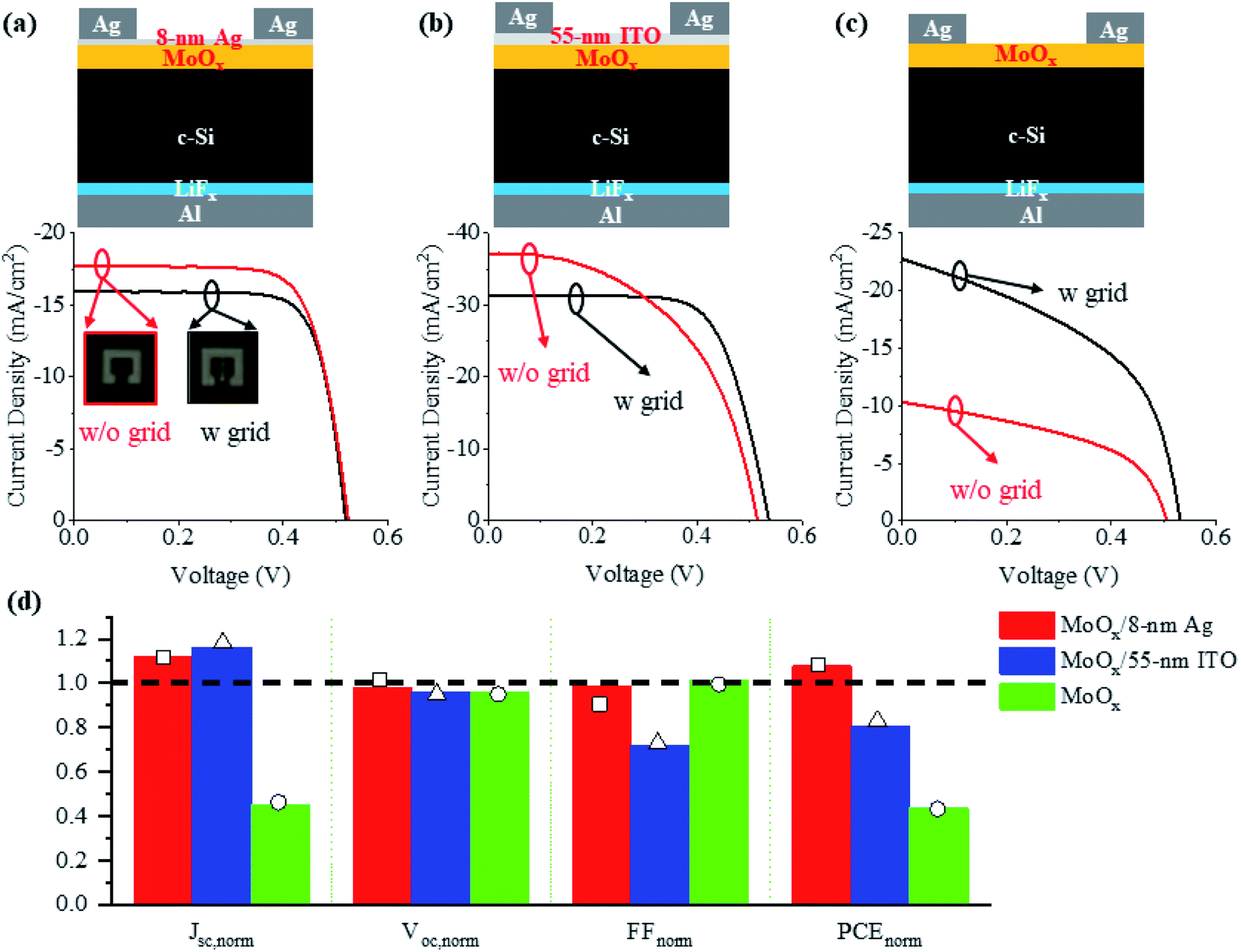 | ||
| Fig. 1 Comparison of c-Si heterojunction solar cells with (a) MoOx/Ag, (b) MoOx/ITO, and (c) pure MoOx as the HSCs: (top) schematic diagrams and (bottom) the best J–V curves for the champion cells with (black) and without (red) grid electrodes. (d) Normalized characteristic parameters, i.e., Jsc,norm, Voc,norm, FFnorm and PCEnorm, calculated from the average values of the three kinds of solar cells without the grid electrodes to those of the counterparts with the grid electrodes. Jsc,norm, Voc,norm, FFnorm and PCEnorm calculated from the values corresponding to the champion PCEs of the three kinds of solar cells are indicated by squares, triangles, and circles, respectively. | ||
| HSCs | Jsc mA cm−2 | Voc mV | FF% | PCE% | Shunt resistance Ω cm2 | Series resistance Ω cm2 | |
|---|---|---|---|---|---|---|---|
| MoOx/Ag | With grid | 15.68 ± 0.29 | 517 ± 1.7 | 75.92 ± 0.1 | 6.16 ± 0.12 | 1724.3 ± 181.8 | 2.96 ± 0.14 |
| 15.92 | 519 | 75.81 | 6.27 | 1828.4 | 3.01 | ||
| Without grid | 17.54 ± 0.61 | 504.7 ± 16.6 | 75.0 ± 1.42 | 6.63 ± 0.17 | 1407.4 ± 294.5 | 2.84 ± 0.82 | |
| 17.69 | 524.4 | 72.99 | 6.77 | 1243.8 | 3.99 | ||
| MoOx/ITO | With grid | 31.35 ± 0.08 | 531 ± 8.5 | 68.75 ± 2.24 | 11.49 ± 0.46 | 658.1 ± 66.1 | 2.75 ± 0.09 |
| 31.28 | 537 | 70.2 | 11.8 | 728.2 | 2.72 | ||
| Without grid | 36.46 ± 0.90 | 510 ± 6.2 | 49.47 ± 3.05 | 9.25 ± 0.92 | 302.1 ± 38.7 | 2.81 ± 0.32 | |
| 37.12 | 515 | 51.29 | 9.81 | 296.8 | 2.67 | ||
| MoOx | With grid | 22.57 ± 0.37 | 529 ± 5.6 | 46.67 ± 1.24 | 5.57 ± 0.17 | 70.1 ± 2.2 | 3.69 ± 0.56 |
| 22.68 | 532 | 47.75 | 5.76 | 68.8 | 3.18 | ||
| Without grid | 10.09 ± 0.2 | 508 ± 7 | 47.2 ± 0.5 | 2.42 ± 0.05 | 141.5 ± 2.3 | 6.76 ± 0.37 | |
| 10.32 | 506 | 47.31 | 2.47 | 140.4 | 6.7 | ||
From Fig. 1a–c, it can be seen that for the grid solar cells, both the MoOx/Ag and MoOx/ITO HSCs enable nearly square J–V curves with large shunt resistances and small series resistances, indicating high fill factors (FFs), in great contrast to the pure MoOx HSC. Especially for the MoOx/Ag HSC grid cell, due to the good conductivity of the ∼8 nm Ag film, the shunt resistance is maximal, leading to a maximum FF of up to 75.92%. However, due to the absorption of the ultrathin Ag film, the transmittance of the MoOx/Ag HSC is lower than those of the MoOx/ITO and the pure MoOx HSCs (Fig. S3, ESI†). This results in a much lower short-circuit current density (Jsc) and thus in a degraded open-circuit voltage (Voc). Therefore, the MoOx/Ag HSC grid solar cell cannot compete with the MoOx/ITO HSC grid solar cell (PCE ∼ 11.49%) but still performs better (PCE ∼ 6.16%) than the pure MoOx HSC grid solar cell (PCE ∼ 5.57%) because of the rather high FF.
When the inner grid is removed from the top electrode, the three solar cells behave differently (Fig. 1a–c). In order to clearly see the changes, the characteristic parameters of the three gridless solar cells were normalized to those of the grid counterparts and are plotted in Fig. 1d. The normalized parameters for the champion solar cells are also indicated in Fig. 1d. Without the shadow of the grid, the illuminated area is increased by about 9% from 23 to 25 mm2. For the MoOx/Ag and MoOx/ITO HSC solar cells, the Jsc values are improved by ∼12% and ∼16%, respectively; while for the pure MoOx HSC solar cell, the Jsc is decreased by ∼55%. This indicates that the double-layer HSCs are much more effective in collecting holes, even those generated in the central illuminated area far from the electrode frame. In contrast, the great reduction in Jsc for the pure MoOx HSC solar cell mainly results from the rather poor conductivity of MoOx. Despite the increased solar illumination and subsequently increased photocarriers, a large number of holes cannot be efficiently extracted by the electrode frame without the inner grid.
Due to the great reduction in Jsc, the Voc is also degraded for the gridless solar cell with the pure MoOx HSC. For the solar cells with the MoOx/Ag and MoOx/ITO HSCs, because the increase in photocarriers and Jsc with the absence of the optical shadows is inevitably accompanied by the increase in carrier recombination, the average Voc decreases a little (Fig. 1d and Table 1). This can be verified by the smaller minority carrier lifetime for the MoOx/Ag- and MoOx/ITO-coated wafers than that for the pure MoOx-coated wafer (demonstrated in Fig. 3a). Fortunately, the Voc degradation is very small for all the solar cells (less than 4%) and does not affect the PCE much. For the gridless MoOx/Ag HSC solar cell with the champion PCE, its Voc is even slightly higher than that of the counterpart with the inner grid electrode (Fig. 1d and Table 1).
For the gridless solar cells with the MoOx/Ag and pure MoOx HSCs, the FFs remain almost unchanged compared with those of the grid cells, but the mechanisms are quite different. In the former, both the shunt and series resistances decrease when the grid is removed. This means that the conductive ultrathin Ag film is favorable for collecting photogenerated holes, but the shunt loss increases without the help of the inner grid for conduction. The opposite behavior happens for the latter because of the less conductive MoOx without the grid, leading to increased shunt and series resistances (Table 1). For the gridless solar cell with the MoOx/ITO HSC, the balance between the hole collection and shunt loss is broken with greatly increased shunt channels. Thus, its FF is greatly reduced (Fig. 1d).
Based on all the above parameters, only the MoOx/Ag HSC can improve the cell PCE (by ∼8%) when the grid is removed. Great PCE degradations of ∼20% and ∼43% are observed when the conventional MoOx/ITO and MoOx HSCs are applied to the gridless solar cells. Unfortunately, the PCE of the gridless MoOx/Ag HSC solar cell is still inferior to that of the gridless MoOx/ITO HSC solar cell due to the much lower Jsc, which is induced by the much lower optical transmissivity of the MoOx/Ag HSC (Fig. S3, ESI†). That being said, the MoOx/Ag HSC is more advantageous in fabrication through thermal evaporation without breaking the vacuum, enabling high-throughput and low-cost fabrication of the whole device. However, to fabricate the MoOx/ITO HSC, pumping twice is necessary for thermal evaporation and sputtering, respectively, which is time-consuming and cost-ineffective. The MoOx/Ag HSC is also more mechanically flexible than the MoOx/ITO HSC, allowing for thin and highly flexible c-Si solar cells as emerging wearable power sources (demonstrated below).
Comprehensive analyses of contact performance
In order to elaborate on the various above photovoltaic behaviors, we characterized the contact performances between the three different HSCs and the n-type c-Si with the transfer length method (TLM).27 As schematically shown in the upper left inset of Fig. 2a, a series of current–voltage curves were measured through two Ag line pads on top of the HSCs with various pad spacings, which are plotted in Fig. 2a–c, respectively, for the MoOx/Ag, MoOx/ITO, and pure MoOx HSCs. All contacts exhibit very good ohmic features. In each panel, the total resistances were also plotted in the lower right inset as a function of the pad spacing and fitted using a straight line, from which the sheet resistance, Rsh_HSC, and the contact resistivity, ρc_HSC, of the HSC were calculated and are plotted in Fig. 2d and e, respectively. Details can be found in Note S2, ESI.† Both the Rsh_HSC and ρc_HSC are drastically reduced when the MoOx film is covered with an ultrathin Ag film or an ITO film and the MoOx/Ag HSC affords the smallest values of Rsh_HSC and ρc_HSC. For all the three HSCs, c-Si is in direct contact with MoOx, which has a much higher workfunction than c-Si. The Fermi level equilibration makes the conduction and valence bands of c-Si bent up near this contact interface, where electrons are blocked and holes are accumulated to form an inversion layer. Such band alignment is beneficial for hole transportation and collection. Therefore, both the measured Rsh_HSC and ρc_HSC include the resistances of the whole HSC and the inversion layer. In order to clearly show how holes are transported from one Ag line pad to another, we present a schematic illustration in Fig. 2f, where there are three channels for hole transport at the c-Si/MoOx/Ag or c-Si/MoOx/ITO contacts. When current is injected from the left Ag line pad, part of the holes first go vertically through the double-layers of the HSC and then flow horizontally in the inversion layer to the right Ag line pad; part of them go through the top Ag or the ITO layer and into the MoOx layer for horizontal transportation; and most holes will flow directly in the top Ag or the ITO layer because of their much better conductivity than MoOx or the inversion layer. Due to the absence of the last highly conductive channel in the pure c-Si/MoOx contact, both vertical and horizontal transportation will meet extremely high resistances. Therefore, for the pure MoOx HSC solar cell, the FF is rather low and a grid is required to collect photogenerated holes, which are otherwise likely to be lost by recombination. Since Ag is more conductive than ITO (to be compared in the next section), the photogenerated holes, which can be collected with lower resistance, can also transport a longer distance. Thus, even for the gridless MoOx/Ag HSC solar cell, the FF still remains very high and the holes are collected efficiently (Fig. 1c and Table 1).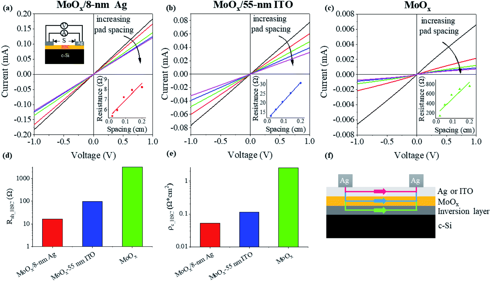 | ||
| Fig. 2 TLM-based HSC/c-Si contact measurement: current–voltage curves between Ag line pad electrodes with different spacings for (a) the MoOx/Ag, (b) the MoOx/ITO, and (c) the pure MoOx HSCs; (d) extracted sheet resistances, Rsh_HSC, and (e) contact resistivities, ρc_HSC, of the three HSCs; (f) schematic diagram of the current flow between two Ag line pad electrodes. | ||
Fig. 3a shows that the measured minority carrier lifetimes of the c-Si wafers covered with the above three HSCs are all higher than that of the individual c-Si wafer. This suggests the passivation effects of the MoOx layer, which is however weakened a little bit by the additional Ag or the ITO layer. As mentioned above, due to the large difference in workfunction, an inversion layer forms near the c-Si/MoOx interface, where holes are accumulated and electrons are blocked. Consequently, carrier recombination here is reduced, which is known as the field-effect passivation of MoOx.49,53 From the field-emission transmission electron microscopy (TEM) image in Fig. 3b, an interlayer can be clearly observed between MoOx and the n-type c-Si regardless of whether MoOx is covered with Ag or ITO. The interlayer thickness is ∼3.98 nm. As reported in our previous work,49,53 this interlayer, containing Mo, O, and Si elements, is mainly due to the oxidization of the c-Si surface and the reduction of the MoOx film. To confirm this point, in this work we explored the interfacial chemical state of the c-Si/MoOx interface through depth profiling X-ray photoelectron spectroscopy (XPS). As shown in Fig. 3e, the O 1s spectrum can be deconvoluted into three dominant peaks associated with Mo–O bonds (531.6 eV), Si–O bonds (532.8 eV), and defective oxide (532.2 eV; inherent to many TMOs56) on the MoOx side. As the etching depth increases, the dominant Mo–O peak drops, while the Si–O peak first increases and then decreases, indicating the oxidization of the Si surface during MoOx deposition. The existence of the oxide interlayer at the MoOx/c-Si interface is also confirmed by the Mo 3d and Si 2p spectra. The Mo 3d spectrum shifts to a lower binding energy, indicating the reduction of Mo6+ cations on the MoOx side to Mo atoms on the c-Si side, while Si is partially oxidized and a mixture of sub-stoichiometric species coexist in the interlayer. It is fully illustrated that the oxide interlayer is caused by the evaporated MoOx, which oxidizes the bottom c-Si surface, making it reduced. The oxide interlayer is able to chemically passivate the dangling bonds of the c-Si surface, further improving the minority carrier lifetime (Fig. 3a).
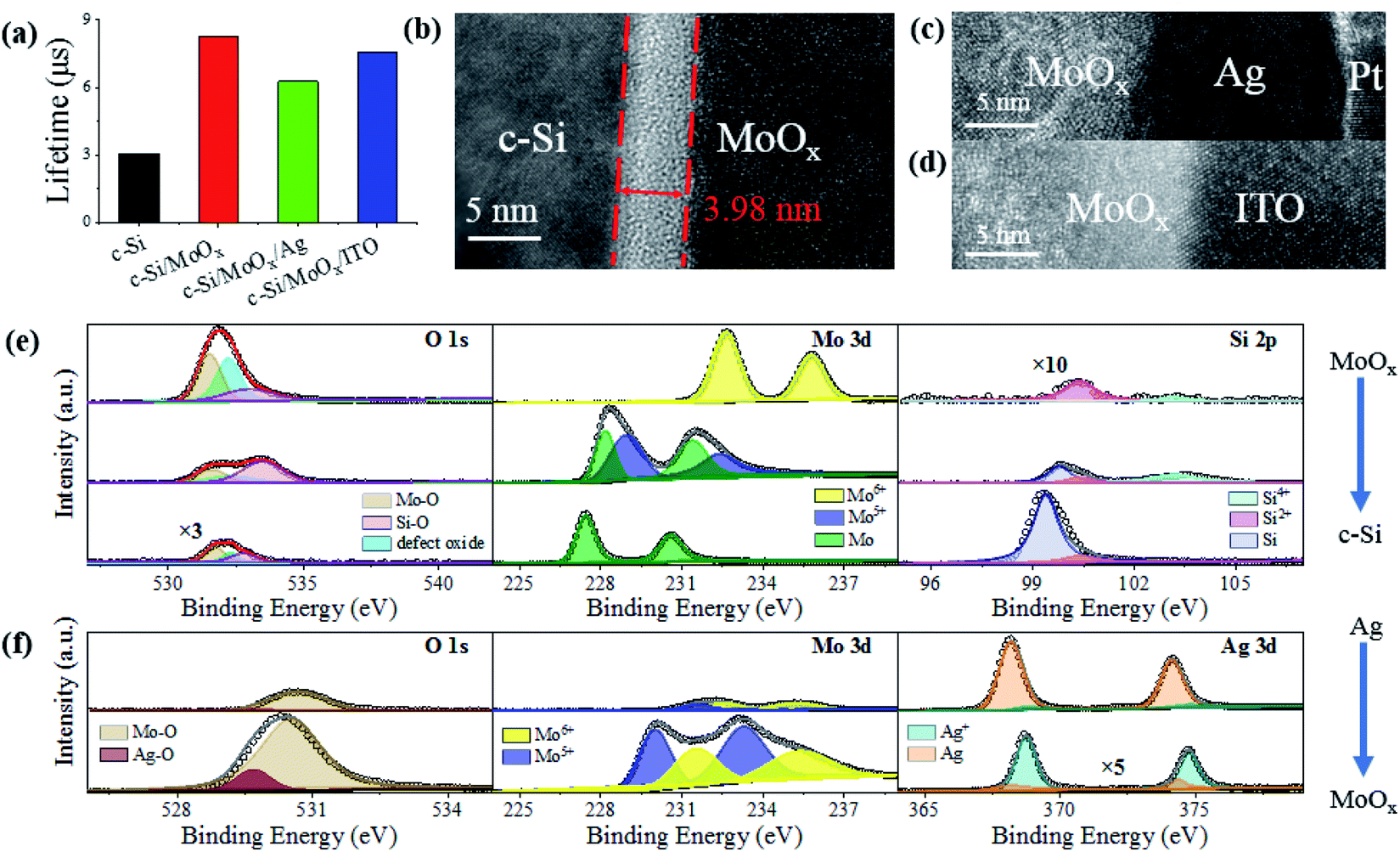 | ||
| Fig. 3 (a) Minority carrier lifetimes of the n-type c-Si, c-Si/MoOx, c-Si/MoOx/Ag, and c-Si/MoOx/ITO samples at an injection level of 1015 cm−3. TEM images of the (b) c-Si/MoOx, (c) MoOx/Ag and (d) MoOx/ITO interfaces. XPS depth profiling results of (e) the c-Si/MoOx interface, showing O 1s, Mo 3d, and Si 2p regions; (f) the MoOx/Ag interface, showing O 1s, Mo 3d, and Si 2p regions (circles: measured; lines: fitted). Some spectra with extremely small intensities are magnified by different multipliers (indicated close to the curves) so as to be distinguished. | ||
In contrast, no apparent interlayers appear at the MoOx/Ag and MoOx/ITO interfaces shown in Fig. 3c and d, respectively. The thermally evaporated ∼8 nm ultrathin Ag film does not look very uniform (whose morphology is demonstrated below) and the interface seems not very flat (Fig. 3c); while the interface between MoOx and the sputtered ITO appears flat, and there is no apparent damage during sputtering (Fig. 3d). In order to further explore the interfacial variation at the MoOx/Ag interface, depth profiling XPS was performed and is illustrated in Fig. 3f. On the Ag side, Ag–O bonds can hardly be distinguished from the O 1s spectrum. However, as the etching depth goes to the MoOx side, the Ag–O peak (529.7 eV) appears clearly, meaning that Ag is likely to be oxidized. From the Mo 3d spectra, it is seen that the main peaks move towards the low binding energy, indicating that part of the Mo6+ ions are reduced to Mo5+ with a significant increase in the intensity on the MoOx side. For the Ag 3d spectra, the dominant peaks are first related to Ag atoms in the outer layer and then become associated with Ag+ cations in the inner layer. These spectral variations illustrate that the initially evaporated Ag is oxidized upon being deposited onto the MoOx film. The remaining Ag atoms at the interface act as recombination centers, leading to a relatively lower carrier lifetime for the c-Si/MoOx/Ag sample compared to that for the c-Si/MoOx/ITO sample, as shown in Fig. 3a. Fortunately, such a lifetime decrease does not cause too much degradation in the Voc for the photovoltaic devices, as shown in Fig. 1 and Table 1.
Effects of Ag thickness on carrier collection in the MoOx/Ag HSC
As a consequence of physical vapor deposition technology, the thermal evaporation of metal films inevitably suffers from the three-dimensional (3D) Volmer–Weber growth mode in the initial stage of deposition.57–61 A continuous film with low resistance cannot be achieved with thickness below 10 nm. A thick film will however lead to rather low optical transparency. Fortunately, MoOx in this work can serve as a seed layer to mitigate the surface energy difference between the Ag to be deposited and the c-Si active layer. The 3D Volmer–Weber growth mode can thus be suppressed effectively, allowing a sub-10 nm Ag continuous film to be achieved with both low sheet resistance and high transmittance.Fig. 4a shows the morphological evolution of our thermally evaporated Ag films with different thicknesses on top of the MoOx-coated c-Si substrates, inspected with scanning electron microscopy (SEM). The thickness-dependent sheet resistances, Rsh_film, and optical transmittance spectra of identical Ag films were characterized on MoOx-coated quartz substrates and are shown in Fig. 4b and S3, ESI,† respectively. All the MoOx coatings were ∼23 nm thick, the same as that applied in solar cells. As shown in Fig. 4a, dense Ag nanoparticles are distributed on the 4 nm thick film. They are separated from each other. Therefore, the Ag film is non-conductive and its Rsh_film is too large to measure. When the film thickness increases to 6 nm, the small Ag nanoparticles become largely isolated nanoclusters. The Rsh_film is measurable but is quite large (Fig. 4b). Upon light illumination, localized surface plasmons (LSPs) are excited in either nanoparticles or nanoclusters,57–61 resulting in enhanced absorption and thus transmission dips around 650 nm (Fig. S3, ESI†). Further increasing the thickness to 8 nm and 10 nm makes the Ag nanoclusters coalesce into sparse and dense networks, respectively. Due to the increased electron transport paths, the Rsh_film drops dramatically to below 10 Ω sq−1, much smaller than that of the ∼55 nm thick ITO (Fig. 4b). Meanwhile, the LPR-induced transmission dips disappear with improved optical transmittance (Fig. S3, ESI†). Among all the ultrathin Ag films, the 8 nm film shows the best transparency (especially in the near-infrared wavelength range) with a sunlight weighted average transmittance of 55.2% but is much lower than those of the ITO or the uncoated pure MoOx films. Fortunately, its rather low Rsh_film enables extremely good carrier collection performance in terms of the sheet resistance and contact resistivity of the HSC on c-Si, to be described below. The small error bars in the Rsh_film at various film thicknesses show the very good repeatability of the deposition process.
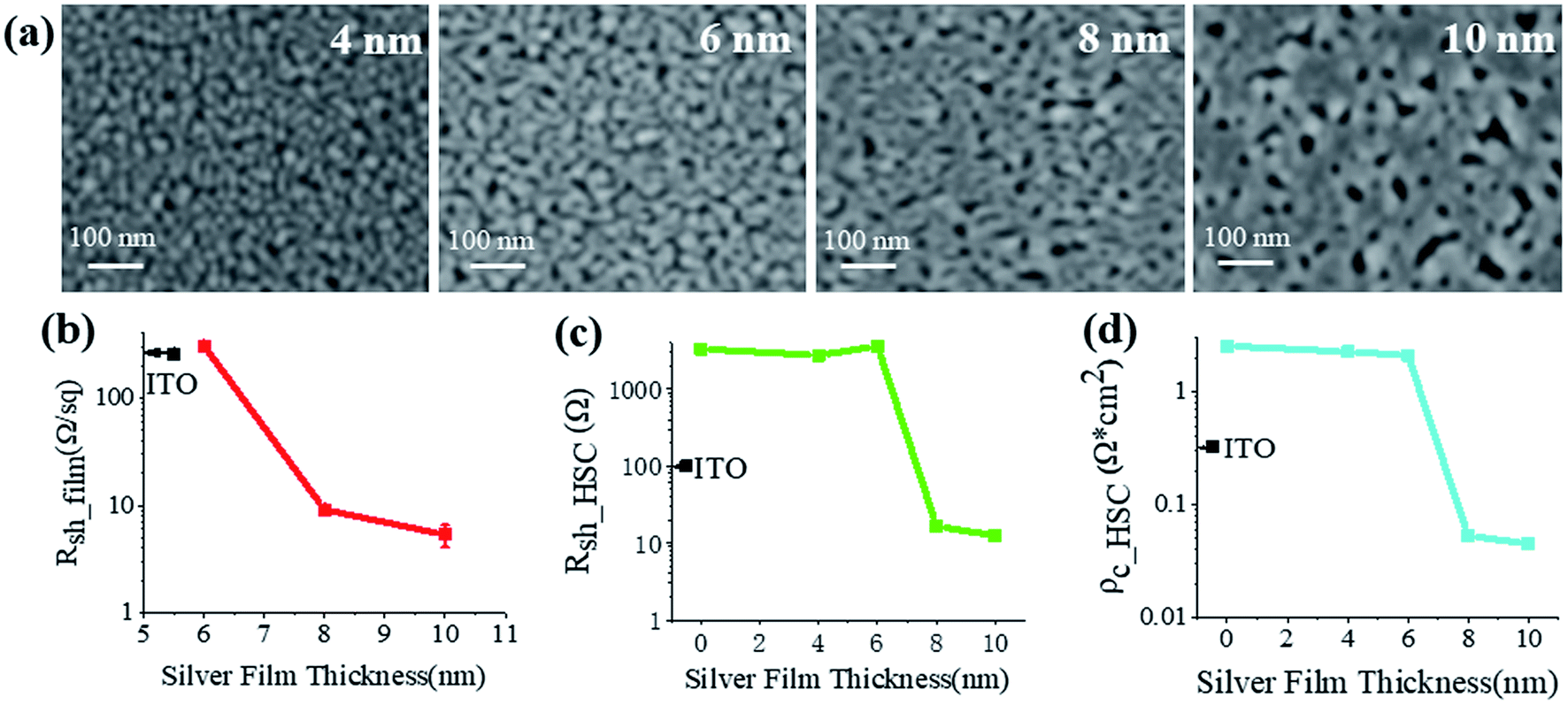 | ||
| Fig. 4 (a) Top view SEM images of our thermally evaporated Ag films with thicknesses of 4, 6, 8, and 10 nm on c-Si/MoOx substrates. (b) Thickness-dependent sheet resistance, Rsh_film, of the identical Ag films deposited on quartz/MoOx substrates. For each value, at least three samples were fabricated and characterized to show the repeatability of the fabrication. (c) Sheet resistance, Rsh_HSC, and (d) contact resistivity, ρc_HSC, of the MoOx/Ag HSC on n-type c-Si as a function of Ag film thickness. For comparison, the corresponding values of Rsh_film, Rsh_HSC, and ρc_HSC for the ∼55 nm thick ITO are also indicated in (b), (c), and (d), respectively. | ||
As shown in Fig. 4c and d, both the sheet resistance, Rsh_HSC, and contact resistivity, ρc_HSC, of the MoOx/Ag HSC follow the trend of the Rsh_film (rather than the optical transparency), dependent on the Ag film thickness (Fig. 4b). Both the Rsh_HSC and ρc_HSC drop dramatically when the Ag film thickness changes from 6 to 8 nm. This strong correlation indicates the dominant role of the ultrathin Ag film on the whole HSC regarding carrier collection. Compared with the pure MoOx HSC, the top Ag film provides another channel to conduct holes. If it is continuous, e.g., in the 8 and 10 nm thick films, the carrier collection can naturally be improved both vertically and horizontally; while for the discontinuous Ag films with thicknesses below 8 nm, both the Rsh_HSC and ρc_HSC show no obvious improvement compared with the pure MoOx HSC (Fig. 4c and d). Due to the large Rsh_film of ITO (Fig. 4b), the MoOx/ITO HSC shows inferior carrier collection ability in terms of its Rsh_HSC (Fig. 4c) and ρc_HSC (Fig. 4d) compared to the MoOx/Ag HSCs with Ag film thicknesses of 8 and 10 nm, whose Ag films are more conductive. It is also found that our MoOx/8 nm Ag HSC owing to a quite low ρc_HSC outperforms almost all the HSCs reported previously (Table S2, ESI†). Therefore, it is believed to be a quite good dopant-free contact for hole collection.
50 μm thick gridless and flexible c-Si solar cell with the MoOx/Ag HSC
In order to further demonstrate the advantage of the MoOx/8 nm Ag HSC, we fabricated flexible c-Si heterojunction solar cells based on 50 μm thick wafers (inset of Fig. 5a), which were etched from 200 μm thick as-bought wafers (Experimental section). For comparison, a 50 μm thick flexible solar cell with the MoOx/55 nm ITO HSC was also fabricated. The J–V curves of the two flexible solar cells are presented in Fig. 5a and compared with those of the 200 μm thick counterparts. Their characteristic parameters were extracted and are listed in Table 2. In order to clearly show the influence of the wafer thickness, the ratios of the characteristic parameters of the 50 μm thick cell to those of the 200 μm thick cell, i.e., Jsc_50/Jsc_200, Voc_50/Voc_200, FF50/FF200, and PCE50/PCE200, were calculated and are plotted in Fig. 5b, where the c-Si thickness ratio, tSi_50/tSi_200, is also indicated for comparison. When the c-Si thickness, tSi, is reduced by 75% from 200 μm to 50 μm, for the MoOx/Ag HSC solar cell, the PCE still retains 86% of the initial value of the 200 μm thick cell with degradation of merely 14%, resulting from the 7%, 4%, and 4% decreases in Jsc, Voc, and FF, respectively (Fig. 5b). However, due to the larger reduction in Jsc (13%) and FF (36%), the PCE decreases more dramatically by 45% for the MoOx/ITO HSC solar cell. Its absolute PCE (5.43%) was even slightly lower than that of the thin MoOx/Ag HSC solar cell (5.85%).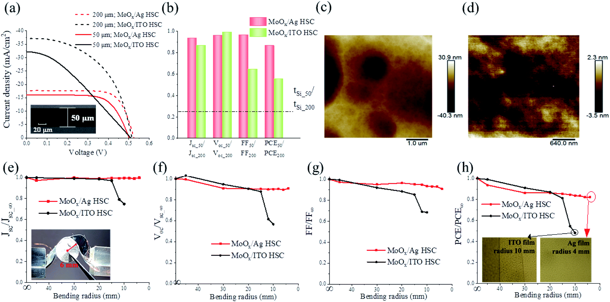 | ||
| Fig. 5 (a) Measured J–V curves of the 50 μm thick gridless c-Si heterojunction solar cells with the MoOx/8 nm Ag and MoOx/55 nm ITO HSCs in comparison with their 200 μm thick counterparts. Inset: SEM image of the 50 μm thick c-Si wafer. (b) Ratios of the characteristic parameters of the 50 μm thick gridless solar cells to those of their 200 μm thick counterparts, i.e., Jsc_50/Jsc_200, Voc_50/Voc_200, FF50/FF200, and PCE50/PCE200. The wafer thickness ratio, tSi_50/tSi_200, is also indicated as a dashed line. Surface morphologies of (c) the etched 50 μm thick and (d) the original 200 μm thick c-Si wafers. Normalized characteristic parameters of the bent gridless solar cells with the MoOx/Ag and MoOx/ITO HSCs to those of the unbent counterparts, i.e., (e) Jsc/Jsc∞, (f) Voc/Voc∞, (g) FF/FF∞, and (h) PCE/PCE∞, as a function of bending radius. The inset in (e) shows a gridless solar cell with the MoOx/Ag HSC bent at a radius of 6 mm; the inset in (h) shows the optical pictures of the 55 nm thick ITO surface after being bent at a radius of 10 mm and of the 8 nm thick Ag film surface after being bent at a radius of 4 mm. | ||
| HSCs | tSi (μm) | Jsc (mA cm−2) | Voc (mV) | FF (%) | PCE (%) | Shunt resistance (Ω cm2) | Series resistance (Ω cm2) |
|---|---|---|---|---|---|---|---|
| MoOx/Ag | 200 | 17.69 | 524.4 | 72.99 | 6.77 | 1243.8 | 3.99 |
| 50 | 16.51 | 503 | 70.43 | 5.85 | 925.93 | 4.79 | |
| MoOx/ITO | 200 | 37.12 | 515 | 51.29 | 9.81 | 298 | 2.67 |
| 50 | 32.19 | 510 | 33.08 | 5.43 | 154.32 | 11.85 |
When the c-Si is thinned, there must be some photons not fully absorbed, especially those in the near-infrared wavelength range. Due to the highly reflective LiFx/Al ESC, they will be reflected towards the front HSC. Since the MoOx/ITO HSC is more transparent than the MoOx/Ag HSC, more light will be transmitted through the MoOx/ITO HSC into the air, leading to larger reflectivity. In contrast, the MoOx/Ag HSC benefits the light trapping62 and thus the reduced reflectivity of the thin cell (Fig. S3 and S4, ESI†). Therefore, the Jsc degradation for the MoOx/Ag HSC solar cell is smaller than that for the MoOx/ITO HSC solar cell (Fig. 5b).
Because of the very fast etching process, the c-Si surface roughness increased from 0.75 nm to 8.02 nm (Fig. 5c and d), which must lead to enhanced carrier recombination at the c-Si surfaces. Fortunately, owing to the good passivation effects of the HSC and ESC, as demonstrated in Fig. 3, in this work and in our previous work,49 the Voc values of both solar cells with the MoOx/Ag and MoOx/ITO HSCs are not affected much by the rough surface. The relatively larger Voc degradation for the MoOx/Ag HSC solar cell is likely due to the Ag atoms occurring at the MoOx/Ag interface as recombination centers, as discussed in Fig. 3. In contrast, the rough c-Si surface seems to affect the quality of the sputtered ITO significantly, leading to a significant increment in the series resistance and an apparent decrease in the shunt resistance of the device (Table 2). Therefore, FF for the MoOx/ITO HSC solar cell drops by 36%, much larger than the FF degradation of 4% for the MoOx/Ag HSC solar cell (Fig. 5b). This indicates the more excellent tolerance of the ultrathin Ag film to the substrate surface to be deposited.
Furthermore, a mechanical flexibility test was conducted for the two kinds of 50 μm thick solar cells with the setup shown in the inset of Fig. 5e. The measured J–V curves of the solar cells under different curvature radii are plotted in Fig. S5, ESI.† To show the performance variation with the curvature radius, the characteristic parameters of the bent solar cells were normalized to those of the unbent cells and are plotted in Fig. 5e–h. It can be seen that all the characteristic parameters for the MoOx/Ag HSC solar cell are above 82% of those for the unbent counterpart, even when the bending radius is reduced to as small as 4 mm. There are no apparent cracks at the Ag surface (inset of Fig. 5g). In great contrast, all the normalized parameters for the MoOx/ITO HSC solar cell fail to remain higher than 80% but instead drop dramatically when the bending radius becomes smaller than 15 mm. We observed obvious cracks at the 55 nm thick ITO surface at a curvature radius of 10 mm (inset of Fig. 5g), which were the main reason for the failure of the MoOx/ITO HSC solar cell at small bending radii. Such a comparison fully illustrates the superior mechanical flexibility of the 8 nm thick Ag film, enabling flexible c-Si solar cells as emerging wearable power sources.
Conclusions
In summary, greatly enhanced hole collection of MoOx has been demonstrated experimentally with a top sub-10 nm thick Ag film, which enables an efficient undoped contacted c-Si heterojunction solar cell without a front grid electrode. Compared with solar cells with front grid electrodes, the gridless solar cell with the MoOx/Ag HSC shows an increment of ∼8% in PCE due to the shadow removal-induced improvement of the Jsc as well as the almost-undiminished FF and Voc, while in great contrast, the gridless solar cells with the conventional MoOx/ITO HSC and pure MoOx HSC exhibit obvious degradations in PCE (∼20% and ∼43%, respectively) due to the overwhelming decrease in their FF and Jsc, respectively. Systematic characterizations of the three HSCs have been conducted. It is found that the more conductive ultrathin Ag film (rather than ITO) provides an additional channel for photogenerated holes to transport more quickly on MoOx, which contributes to the great enhancement in hole collection and shunt loss suppression in the gridless solar cells. Our MoOx/Ag double-layer HSC can be easily fabricated through thermal evaporation without breaking the vacuum, saving both the time and cost of the fabrication of the whole device. Based on this HSC, a 50 μm thick gridless c-Si heterojunction solar cell is demonstrated, which is 75% thinner but retains 86% of the PCE of its 200 μm thick counterpart (while the 50 μm thick gridless solar cell with the MoOx/ITO HSC is much less efficient). It is over 82% efficient after being bent to a curvature radius as small as 4 mm, showing much better mechanical flexibility than its counterpart with the MoOx/ITO HSC. This work provides a guide for the design of high-efficiency and low-cost solar cells, promising for applications as emerging wearable power sources.Conflicts of interest
There are no conflicts to declare.Acknowledgements
This work was supported in part by the National Natural Science Foundation of China (91833303, 61775195), National Key Research and Development Program of China (2017YFA0205700), Fundamental Research Funds for the Central Universities (Zhejiang University NGICS Platform), and Ningbo Science and Technology Project (2018B10093).Notes and references
- C. Battaglia, A. Cuevas and S. De Wolf, Energy Environ. Sci., 2016, 9, 1552–1576 RSC.
- T. G. Allen, J. Bullock, X. Yang, A. Javey and S. De Wolf, Nat. Energy, 2019, 4, 914–928 CrossRef CAS.
- Y. Liu, Y. Li, Y. Wu, G. Yang, L. Mazzarella, P. Procel-Moya, A. Tamboli, K. Weber, M. Boccard, O. Isabella, X. Yang and B. Sun, Mater. Sci. Eng. R, 2020, 142, 100579 CrossRef.
- A. Richter, R. Müller, J. Benick, F. Feldmann, B. Steinhauser, C. Reichel, A. Fell, M. Bivour, M. Hermle and S. W. Glunz, Nat. Energy, 2021, 6, 429–438 CrossRef CAS.
- F. Haase, C. Hollemann, S. Schäfer, A. Merkle, M. Rienäcker, J. Krügener, R. Brendel and R. Peibst, Sol. Energy Mater. Sol. Cells, 2018, 186, 184–193 CrossRef CAS.
- K. Yoshikawa, H. Kawasaki, W. Yoshida, T. Irie, K. Konishi, K. Nakano, T. Uto, D. Adachi, M. Kanematsu, H. Uzu and K. Yamamoto, Nat. Energy, 2017, 2, 17032 CrossRef CAS.
- A. Richter, S. W. Glunz, F. Werner, J. Schmidt and A. Cuevas, Phys. Rev. B: Condens. Matter Mater. Phys., 2012, 86, 165202 CrossRef.
- D. Yan and A. Cuevas, J. Appl. Phys., 2014, 116, 194505 CrossRef.
- J. Oh, H.-C. Yuan and H. M. Branz, Nat. Nanotechnol., 2012, 7, 743–748 CrossRef CAS PubMed.
- S. C. Baker-Finch, K. R. McIntosh, D. Yan, K. C. Fong and T. C. Kho, J. Appl. Phys., 2014, 116, 063106 CrossRef.
- A. Descoeudres, C. Allebé, N. Badel, L. Barraud, J. Champliaud, G. Christmann, F. Debrot, A. Faes, J. Geissbühler, J. Horzel, A. Lachowicz, J. Levrat, S. Martin de Nicolas, S. Nicolay, B. Paviet-Salomon, L. L. Senaud, C. Ballif and M. Despeisse, Sol. Energy, 2018, 175, 54–59 CrossRef CAS.
- J. Melskens, B. W. H. v. d. Loo, B. Macco, L. E. Black, S. Smit and W. M. M. Kessels, IEEE J. Photovolt., 2018, 8, 373–388 Search PubMed.
- T. G. Allen, J. Bullock, P. Zheng, B. Vaughan, M. Barr, Y. Wan, C. Samundsett, D. Walter, A. Javey and A. Cuevas, Prog. Photovoltaics, 2017, 25, 636–644 CAS.
- Y. Wan, C. Samundsett, D. Yan, T. Allen, J. Peng, J. Cui, X. Zhang, J. Bullock and A. Cuevas, Appl. Phys. Lett., 2016, 109, 113901 CrossRef.
- B. Liao, B. Hoex, A. G. Aberle, D. Chi and C. S. Bhatia, Appl. Phys. Lett., 2014, 104, 253903 CrossRef.
- G. Sahasrabudhe, S. M. Rupich, J. Jhaveri, A. H. Berg, K. A. Nagamatsu, G. Man, Y. J. Chabal, A. Kahn, S. Wagner, J. C. Sturm and J. Schwartz, J. Am. Chem. Soc., 2015, 137, 14842–14845 CrossRef CAS PubMed.
- X. Yang, P. Zheng, Q. Bi and K. Weber, Sol. Energy Mater. Sol. Cells, 2016, 150, 32–38 CrossRef CAS.
- Y. Wan, C. Samundsett, J. Bullock, M. Hettick, T. Allen, D. Yan, J. Peng, Y. Wu, J. Cui, A. Javey and A. Cuevas, Adv. Energy Mater., 2017, 7, 1601863 CrossRef.
- Z. Yang, P. Gao, J. Sheng, H. Tong, C. Quan, X. Yang, K. W. A. Chee, B. Yan, Y. Zeng and J. Ye, Nano Energy, 2018, 46, 133–140 CrossRef CAS.
- J. Bullock, P. Zheng, Q. Jeangros, M. Tosun, M. Hettick, C. M. Sutter-Fella, Y. Wan, T. Allen, D. Yan, D. Macdonald, S. De Wolf, A. Hessler-Wyser, A. Cuevas and A. Javey, Adv. Energy Mater., 2016, 6, 1600241 CrossRef.
- H.-D. Um, N. Kim, K. Lee, I. Hwang, J. H. Seo and K. Seo, Nano Lett., 2016, 16, 981–987 CrossRef CAS PubMed.
- J. Bullock, M. Hettick, J. Geissbühler, A. J. Ong, T. Allen, C. M. Sutter-Fella, T. Chen, H. Ota, E. W. Schaler, S. De Wolf, C. Ballif, A. Cuevas and A. Javey, Nat. Energy, 2016, 1, 15031 CrossRef CAS.
- Y. Wan, C. Samundsett, J. Bullock, T. Allen, M. Hettick, D. Yan, P. Zheng, X. Zhang, J. Cui, J. McKeon, A. Javey and A. Cuevas, ACS Appl. Mater. Interfaces, 2016, 8, 14671–14677 CrossRef CAS.
- Z. Wang, P. Li, Z. Liu, J. Fan, X. Qian, J. He, S. Peng, D. He, M. Li and P. Gao, APL Mater., 2019, 7, 110701 CrossRef.
- C. Battaglia, X. Yin, M. Zheng, I. D. Sharp, T. Chen, S. McDonnell, A. Azcatl, C. Carraro, B. Ma, R. Maboudian, R. M. Wallace and A. Javey, Nano Lett., 2014, 14, 967–971 CrossRef CAS PubMed.
- C. Battaglia, S. M. de Nicolás, S. De Wolf, X. Yin, M. Zheng, C. Ballif and A. Javey, Appl. Phys. Lett., 2014, 104, 113902 CrossRef.
- J. Bullock, A. Cuevas, T. Allen and C. Battaglia, Appl. Phys. Lett., 2014, 105, 232109 CrossRef.
- J. Geissbühler, J. Werner, S. Martin de Nicolas, L. Barraud, A. Hessler-Wyser, M. Despeisse, S. Nicolay, A. Tomasi, B. Niesen, S. De Wolf and C. Ballif, Appl. Phys. Lett., 2015, 107, 081601 CrossRef.
- L. G. Gerling, S. Mahato, A. Morales-Vilches, G. Masmitja, P. Ortega, C. Voz, R. Alcubilla and J. Puigdollers, Sol. Energy Mater. Sol. Cells, 2016, 145, 109–115 CrossRef CAS.
- M. Bivour, J. Temmler, H. Steinkemper and M. Hermle, Sol. Energy Mater. Sol. Cells, 2015, 142, 34–41 CrossRef CAS.
- C. Liu, L. Zhang, G. Yu, T. Wang, X. Wu, L. Xu, P. Lin, C. Cui, X. Yu and P. Wang, Mater. Sci. Semicond. Process., 2022, 146, 106687 CrossRef CAS.
- M. Nayak and V. K. Komarala, IEEE Trans. Electron Devices, 2022, 69, 3251–3257 Search PubMed.
- W. Wang, J. He, D. Yan, W. Chen, S. P. Phang, C. Samundsett, S. K. Karuturi, Z. Li, Y. Wan and W. Shen, Sol. Energy, 2022, 231, 203–208 CrossRef CAS.
- J. Chen, C. Liu, S. Xu, P. Wang, X. Ge, B. Han, Y. Zhang, M. Wang, X. Wu, L. Xu, P. Lin, X. Huang, X. Yu and C. Cui, Mater. Sci. Semicond. Process., 2021, 132, 105920 CrossRef CAS.
- M. Gülnahar, H. Nasser, A. Salimi and R. Turan, J. Mater. Sci.: Mater. Electron., 2021, 32, 1092–1104 CrossRef.
- C. Lu, Rusli, A. B. Prakoso and Z. Li, Mater. Chem. Phys., 2019, 236, 121779 CrossRef CAS.
- T. Pan, J. Li, Y. Lin, Z. Xue, Z. Di, M. Yin, J. Wang, L. Lu, L. Yang and D. Li, J. Mater. Sci.: Mater. Electron., 2021, 32, 3475–3486 CrossRef CAS.
- Y. Jiang, S. Cao, L. Lu, G. Du, Y. Lin, J. Wang, L. Yang, W. Zhu and D. Li, Nanoscale Res. Lett., 2021, 16, 87 CrossRef CAS.
- G. Gregory, C. Luderer, H. Ali, T. S. Sakthivel, T. Jurca, M. Bivour, S. Seal and K. O. Davis, Adv. Mater. Interfaces, 2020, 7, 2000895 CrossRef CAS.
- H. Nasser, F. Es, M. Z. Borra, E. Semiz, G. Kökbudak, E. Orhan and R. Turan, Prog. Photovoltaics, 2021, 29, 281–293 CAS.
- D. Xu, X. Yu, D. Gao, C. Li, M. Zhong, H. Zhu, S. Yuan, Z. Lin and D. Yang, J. Mater. Chem. A, 2016, 4, 10558–10565 RSC.
- G. Masmitjà, L. G. Gerling, P. Ortega, J. Puigdollers, I. Martín, C. Voz and R. Alcubilla, J. Mater. Chem. A, 2017, 5, 9182–9189 RSC.
- X. Yang, H. Xu, W. Liu, Q. Bi, L. Xu, J. Kang, M. N. Hedhili, B. Sun, X. Zhang and S. De Wolf, Adv. Electron. Mater., 2020, 6, 2000467 CrossRef CAS.
- G. Masmitjà, E. Ros, R. Almache-Hernández, B. Pusay, I. Martín, C. Voz, E. Saucedo, J. Puigdollers and P. Ortega, Sol. Energy Mater. Sol. Cells, 2022, 240, 111731 CrossRef.
- Z. Liu, W. Lin, Z. Chen, D. Chen, Y. Chen, H. Shen and Z. Liang, Adv. Mater. Interfaces, 2022, 9, 2102374 CrossRef CAS.
- Z. Xu, S. Peng, H. Lin, S. Tian, Z. Wang, J. He, L. Cai, J. Hou and P. Gao, Sol. RRL, 2021, 5, 2100064 CrossRef CAS.
- J. Bullock, Y. Wan, Z. Xu, S. Essig, M. Hettick, H. Wang, W. Ji, M. Boccard, A. Cuevas, C. Ballif and A. Javey, ACS Energy Lett., 2018, 3, 508–513 CrossRef CAS.
- W. Wu, W. Lin, S. Zhong, B. Paviet-Salomon, M. Despeisse, Q. Jeangros, Z. Liang, M. Boccard, H. Shen and C. Ballif, Phys. Status Solidi RRL, 2020, 14, 1900688 CrossRef CAS.
- H. Dai, L. Yang and S. He, Nano Energy, 2019, 64, 103930 CrossRef CAS.
- W. Wu, J. Bao, Z. Liu, W. Lin, X. Yu, L. Cai, B. Liu, J. Song and H. Shen, Mater. Lett., 2017, 189, 86–88 CrossRef CAS.
- H. T. Nguyen, E. Ros, T. Tom, J. Bertomeu, J. M. Asensi, J. Andreu, I. M. Garcia, P. Ortega, M. Garín, J. Puigdollers, C. Voz and R. Alcubilla, IEEE J. Photovolt., 2019, 9, 72–77 Search PubMed.
- O. Akdemir, M. Z. Borra, H. Nasser, R. Turan and A. Bek, Int. J. Energy Res., 2020, 44, 3098–3109 CrossRef CAS.
- N. Lu, Q. Lei, X. Xu, L. Yang, Z. Yang, Z. Liu, Y. Zeng, J. Ye and S. He, Opt. Express, 2022, 30, 21309–21323 CrossRef CAS.
- L. Shi, Y. Cui, Y. Gao, W. Wang, Y. Zhang, F. Zhu and Y. Hao, Nanomaterials, 2018, 8, 473–485 CrossRef PubMed.
- R. A. Sinton and A. Cuevas, Appl. Phys. Lett., 1996, 69, 2510–2512 CrossRef CAS.
- L. G. Gerling, C. Voz, R. Alcubilla and J. Puigdollers, J. Mater. Res., 2017, 32, 260–268 CrossRef CAS.
- C. Zhang, C. Ji, Y.-B. Park and L. J. Guo, Adv. Opt. Mater., 2021, 9, 2001298 CrossRef CAS.
- Y.-G. Bi, Y.-F. Liu, X.-L. Zhang, D. Yin, W.-Q. Wang, J. Feng and H.-B. Sun, Adv. Opt. Mater., 2019, 7, 1800778 CrossRef.
- J. Yun, Adv. Funct. Mater., 2017, 27, 1606641 CrossRef.
- X. He, Q. Cao, J. Pan, L. Yang and S. He, RSC Adv., 2021, 11, 11481–11489 RSC.
- X. He, L. Yang and S. He, Opt. Lett., 2021, 46, 4666–4669 CrossRef CAS PubMed.
- N. P. Sergeant, A. Hadipour, B. Niesen, D. Cheyns, P. Heremans, P. Peumans and B. P. Rand, Adv. Mater., 2012, 24, 728–732 CrossRef CAS.
Footnotes |
| † Electronic supplementary information (ESI) available. See https://doi.org/10.1039/d2ra01512a |
| ‡ These authors contributed equally to this work. |
| This journal is © The Royal Society of Chemistry 2022 |