DOI:
10.1039/D2RA01394K
(Paper)
RSC Adv., 2022,
12, 20850-20856
Silicon micron cages derived from a halloysite nanotube precursor and aluminum sacrificial template in molten AlCl3 as an anode for lithium-ion batteries†
Received
2nd March 2022
, Accepted 16th May 2022
First published on 21st July 2022
Abstract
Porous nanostructures have been proposed a promising strategy to improve the electrochemical performance of Si materials as anodes of lithium-ion batteries (LIBs). However, expensive raw materials and the tedious preparation processes hinder their widespread adoption. In this work, silicon micron cages (SMCs) have been synthesized in molten AlCl3 through using spherical aluminum particles as a sacrificial template, and the earth-abundant and low-cost natural halloysite clay as a precursor. The aluminum spheres (1–3 μm) not only act as a sacrificial template but also facilitate the formation of silicon branches, which connect together to form SMCs. As anodes for LIBs, the SMC electrode exhibits a high reversible capacity of 1977.5 mA h g−1 after 50 cycles at a current density of 0.2 A g−1, and 1035.1 mA h g−1 after 300 cycles at a current density of 1.0 A g−1. The improved electrochemical performance of SMCs could be ascribed to the micron cage structure, providing abundant buffering space and mesopores for Si expansion. This promising method is expected to offer a pathway towards the scalable application of Si-based anode materials in the next-generation LIB technology.
Introduction
Silicon, with a theoretical lithium storage capacity (3580 mA h g−1) of nearly 10 times that of the graphite anode material (372 mA h g−1), is one of the most promising candidates for the next generation of lithium-ion batteries (LIBs). The attractive properties including low operational voltage, high earth abundance and low toxicity are additional benefits for silicon used as an anode material. Compared with the conventional electrode materials with relatively small structural changes during lithiation and delithiation, silicon suffers from large volume changes up to 300% due to the insertion/extraction of Li during every cycle. The instability of the solid-electrolyte interphase (SEI) caused by volume change and side reactions with the electrolyte, as well as the capacity fading caused by particle fracture and poor contact with current collector hinder its widespread adoption. Several strategies, including nanostructure anodes materials, nanocomposites of anode materials, surface modification of electrode and porous structures of anode materials, have been proposed to promote the electrochemical performance of silicon-based anode materials. Among these strategies, porous structure can provide buffering space for the volume expansion and optimize the Li-ion diffusion path, making it a promising strategy to improve the cycling performance and rate capability of silicon-based anode materials.1 Template methods, as is one of the most favorable methods, is widely used to synthesis porous silicon. A series of materials such as alumina,2 silica3 and graphene4 have been used as template to synthesis silicon nanotubes, silicon hollow nanospheres and silicon nanosheets, etc. The capacity, cycling performance and rate capability of silicon anode materials prepared using template have been significantly improved. However, porous silicon anode materials reported previously were mostly derived from the reduction of commercial SiO2 nanosphere/particle or chemical etching of commercial Si or Si/Al nano/micron particles, all of which require expensive raw materials and tedious preparation processes.3,5 Recently, natural aluminosilicate clay minerals have been used as precursor to synthesis silicon anode material via magnesiothermic/aluminothermic reduction for their nano structure and low cost. Huang et al., synthesized porous silicon/carbon (pSi/C) composite nanosheets by reducing the carbon-coated expanded vermiculite with metallic Al in the molten salts.6 The anode of pSi/C nanosheets exhibited a reversible capacity of 1837 mA h g−1 at 4 A g−1 after 500 cycles. Chen et al., prepared self-templating one-dimensional (1D) silicon nanorods from natural sepiolite by magnesiothermic reduction.7 Zhang et al., reported hierarchically porous micron-sized Si particles derived from the low-cost diatomite precursor. 90% capacity can be retained after 500 cycles at 0.2C for the sample without any coating or prelithiation.8 Halloysite is one of the natural clay minerals with a tubular morphology and a chemical formula of Al2Si2O5(OH)4·2H2O. The inner, external diameter and length of halloysite monomer tubes are about 15–100 nm, 40–190 nm and 500–1000 nm, respectively. Abundant resources, industrial supply, as well as low price make halloysite an excellent source of silicon. Various silicon structures such as Si nanoparticles,9 interconnected Si nanoparticles10 and 3D interconnected Si frameworks11 have been synthesized using acid etched natural halloysite nanotubes through the magnesiothermic reduction process. This indicates that delicate structures can be designed when preparing silicon materials using natural clay minerals as precursors through magnesiothermic/aluminothermic reduction. In this work, we proposed that aluminum metal nanospheres (diameter ≈ 2 μm) and H-aSiO2 (Halloysite-amorphous SiO2: acid selective etched natural halloysite nanotubes) can be used as sacrificial template and Si precursor, respectively. Silicon-micron-cages (SMCs) are further synthesized successfully through aluminothermic reduction in the molten salts. Using as anode of LIBs, compared with commercial silicon (C–Si) material, SMCs exhibit outstanding lithium storage performance due to the meticulous structure design. Another aluminothermic reduction of H-aSiO2 was conducted as comparative study using the same method except for aluminum with larger particle diameter of 100–200 μm to confirm the sacrificial template role of the aluminum metal nanospheres.
Experiments
Synthesis of silicon micron cages (SMCs)
Chemical compounds used in this article. Chlorohydric acid (PubChem CID: 313), (36%, AR); hydrofluoric acid (PubChem CID: 14917), (40%, AR); ethanol (PubChem CID: 702), (99.5%, AR); aluminum powder (1–2 μm) (PubChem CID: 5359268); aluminum powder (100–200 μm) (PubChem CID: 5359268); aluminum chloride (PubChem CID: 24012), (99%, AR); commercial silicon (diameter: 2 μm) (PubChem CID: 5461123). All the reagents used in this study were purchased from Sinopharm (Shanghai, China). The natural halloysite clay used in this work was provided by Hunan Xianglei Kaolin Industrial Co., Ltd.
Preparation of H-aSiO2. Typically, 4 g of halloysite powder was well dispersed in a hydrochloric acid solution (6 M, 40 mL) and transferred into a 100 mL Teflon autoclave. The dispersion was acid treated at 160 °C for 4 h. After cooling down to room temperature, the white precipitates were collected with a filter and washed three times with deionized water and ethanol, respectively. The collections were dried in oven at 110 °C for 6 h. The halloysite-derived aSiO2 (amorphous SiO2) samples were labeled as H-aSiO2.
Aluminothermic reduction. Fig. 1 shows the schematic illustration of the synthesis of silicon micron cages (SMCs). The aluminothermic reduction of H-aSiO2 obeys: 4Al + 3SiO2 + 2AlCl3→3Si + 6AlOCl. 2 g of H-aSiO2 was mixed well with 2.5 g Al powder and 16 g AlCl3 in air in a 100 mL Teflon autoclave. Then, the autoclave was sealed immediately and heated in an oven at 240 °C for 20 h. After cooling to room temperature naturally, the resultant was washed with 1 mol L−1 HCl/HF in a 100 mL Plastic beaker with a magnetic stirrer for 1 h. Sample denoted SMCs was obtained after washed with distilled water three times and dried in vacuum oven at 110 °C for 10 h. In order to investigate the formation mechanism of SMCs, silicon was prepared using the same process with larger diameter aluminum particles (100–200 μm). The silicon material prepared as a comparative study was denoted as COM-Si.
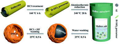 |
| | Fig. 1 Schematic illustration of the synthesis of silicon micron cages (SMCs). | |
Material characterization
The structure and morphology of the product were characterized by X-ray diffractometer (Rigaku D/Max-2400), Raman spectrometer (Renishaw, RM-1000), X-ray photoelectron spectroscopy (XPS) (Kratos Analytical Ltd AXIS Supra), nitrogen adsorption isotherms (Mocromeritics ASAP 2020 analyzer), Scanning electron microscopy (FEI Nova NanoSEM 430, 15 kV, 176 μA) and Transmission electron microscopy (FEI Tecnai F20).
Electrochemical measurements
The electrochemical properties of SMCs and C–Si were evaluated through coin type cells (2016 R-type) which were assembled under an argon-filled glove box (H2O, O2 < 1 ppm). The metallic Li sheet was used as a counter electrode. 1 M LiPF6 in a mixture of ethylene carbonate (EC)/dimethyl carbonate (DEC)/diethylene carbonate (DMC) = 1![[thin space (1/6-em)]](https://www.rsc.org/images/entities/char_2009.gif) :1:1 in volume with 5 wt% fluoroethylene carbonate (FEC) was used as electrolyte. For preparing working electrode, the slurry mixed with as-prepared SMCs material, carbon black (super P) and sodium alginate (SA) binder in a weight ratio of 6:2:2 in water solvent was pasted onto a Cu foil, and then dried in a vacuum oven at 80 °C for 10 h. The active material density of each electrode was determined to be about 1.0 mg cm−2. Galvanostatic measurements were conducted using a LAND-CT2001A instrument at room temperature with a fixed voltage range of 0.005–1.5 V (vs. Li/Li+). Cyclic voltammetry (CV) was performed on electrochemistry workstation (CHI660D), with a scanning rate of 0.1 mV s−1 at room temperature.
:1:1 in volume with 5 wt% fluoroethylene carbonate (FEC) was used as electrolyte. For preparing working electrode, the slurry mixed with as-prepared SMCs material, carbon black (super P) and sodium alginate (SA) binder in a weight ratio of 6:2:2 in water solvent was pasted onto a Cu foil, and then dried in a vacuum oven at 80 °C for 10 h. The active material density of each electrode was determined to be about 1.0 mg cm−2. Galvanostatic measurements were conducted using a LAND-CT2001A instrument at room temperature with a fixed voltage range of 0.005–1.5 V (vs. Li/Li+). Cyclic voltammetry (CV) was performed on electrochemistry workstation (CHI660D), with a scanning rate of 0.1 mV s−1 at room temperature.
Results and discussion
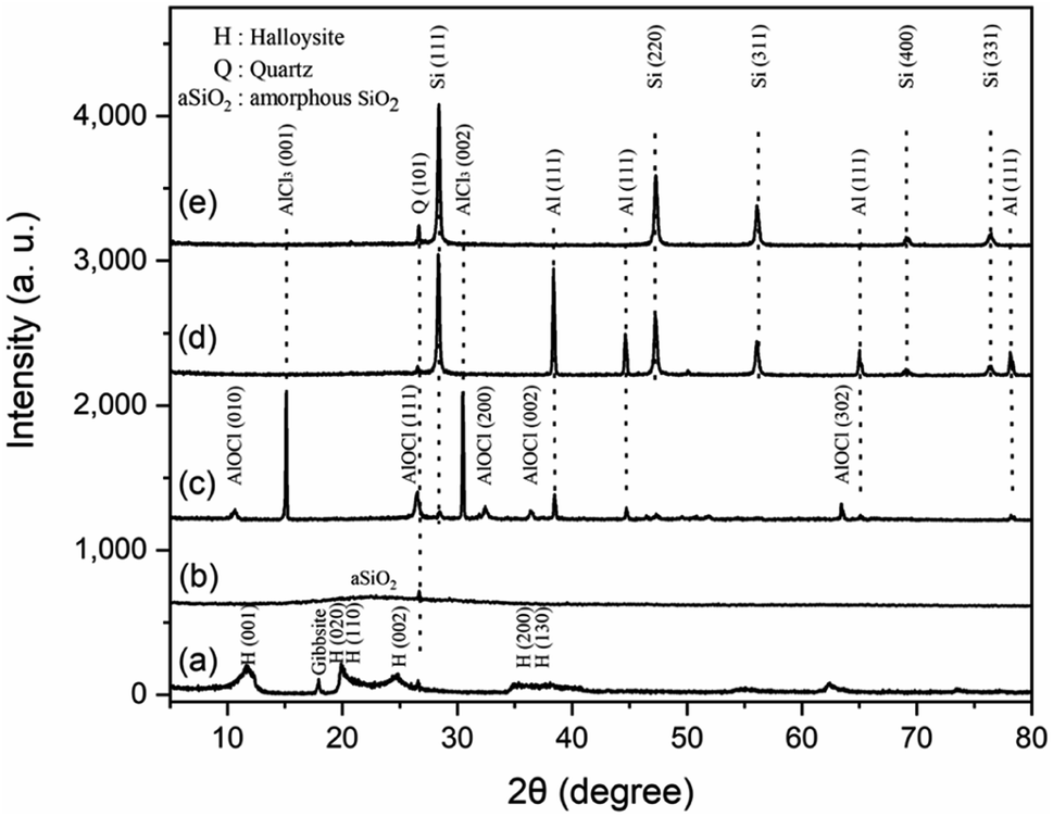
Fig. 2 shows the XRD patterns for products in all steps of preparation. The XRD pattern of natural halloysite clay matches well with the standard card of the Halloysite-7 Å (JCPDS No. 29-1487) (Fig. 2a). The peaks at 2θ = 18.3° and 26.6°, corresponding to gibbsite12 and quartz,13 respectively, indicates the impurity of natural halloysite clay. The main composite of gibbsite is Al(OH)3, which can be easily removed by HCl solution during the acid etching process. The inner layer of alumina was etched during HCl treatment, resulting in the loss of the multilayer wall packing structure. The peaks of halloysite are displaced by a broad and weak peak in the 2θ range of 15–35°, suggesting amorphous SiO2 (ref. 10) (Fig. 2b). A weak peak at 2θ = 26.7°, corresponding to quartz, can also be found in previous reports.13,14 In this work, quartz comes mainly from the raw halloysite clay, for the undissolvable of quartz in HCl solution. Fig. 2c depicts the XRD pattern of crud products without any washing. AlCl3, AlOCl, Al and Si are detected, which is well matched with the previous study.15 The presence of AlCl3 and metallic Al is attributed to the excess reagents. AlOCl was generated from the reaction of AlCl3 and Al2O3.16 Al2O3 is the by-product of the reduction of silicon from aluminum. After water washing (Fig. 2d), the main proportion of crud products are Al and Si, indicating AlCl3 and AlOCl can be removed by water. After 1 mol L−1 HCl/HF solution washing, the peaks located at 28.56°, 47.44°, 56.25°, 69.3°, and 76.51° are indexed to the diffraction peaks of the 111, 220, 311, 400 and 331 lattice planes of the cubic Si (JCPDS No. 27-1402) (Fig. 2e), indicating the crystalline silicon was successfully synthesized. The weak peak at 2θ = 26.7° observed in Fig. 2d and e may correspond to quartz coming from the raw halloysite clay.
 |
| | Fig. 2 XRD patterns for products in each step of preparing silicon micron cages (SMCs). (a) Halloysite clay; (b) H-aSiO2: halloysite etched by HCl; (c) crud products without any washing; (d) crud products after water washing; (e) Si products etched by 1 mol L−1 HCl/HF solution. | |
The SEM images of products in each preparation stage are displayed in Fig. 3a–f. The halloysite clay possessing 500–1000 nm and 50 nm for length and outer diameter, respectively, shows the uniform nanotubes and smooth surface (Fig. 3a). Although the tubular morphology of halloysite maintained after acid etching, the diameter shrunk and the surface is rough (Fig. 3b), resulting from the removal of aluminum oxide octahedron in the inner layer of halloysite by HCl etching. The aluminum particles (1–3 μm) and H-aSiO2 were evenly mixed (Fig. 3c), conducive to the progression of reduction. The crud product without any washing after reduction shows the spherical particles encased in irregular mass (Fig. 3d), composed of AlCl3, AlOCl, Al and Si informed by the results of XRD. After AlCl3, AlOCl removed with water, spherical particles with a diameter of 1–3 μm are the mixture of Si and Al particles (Fig. 3e). In the last step, spherical silicon particles will be obtained after the 1 mol L−1 HCl/HF solution treatment (Fig. 3f).
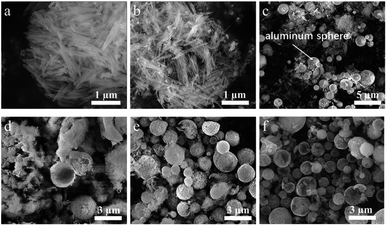 |
| | Fig. 3 SEM images for products in each step of preparing silicon micron cages (SMCs). (a) Halloysite clay; (b) H-aSiO2: HCl etched halloysite; (c) the mixture of Al and H-aSiO2 before reducing; (d) crud products without any washing after the reduction; (e) crud products after water washing; (f) silicon products after 1 mol L−1 HCl/HF solution washing. | |
Fig. 4a and b show the magnified images of prepared silicon material. The spherical silicon particle with slit is assembled from silicon branches and is found to be hollow. The silicon material prepared in this work is denoted as silicon micron cages (SMCs) for the similar structure to cage. The inner surface of SMCs is rough, and the wall thickness of SMC is about 100 nm (Fig. 4c). The hollow structure with slit of SMC can be clearly observed through transmission electron microscopy (TEM) (Fig. 4d). The high-resolution transmission electron microscopy (HRTEM) image in Fig. 4e demonstrates an amorphous SiO2 with a thickness of about 3 nm covering the crystal silicon, indicating the oxidation of silicon. The overhang portion of silicon has been completely oxidized into amorphous SiO2. The inset image of Fig. 4e shows the homogeneous lattice fringes with a spacing 0.31 nm, corresponding to the (111) plane of the cubic Si. The crystallinity of SMCs was further verified by selected area electron diffraction (SAED) (Fig. 4f). The diffraction rings could be indexed to the (111), (220) and (311) planes of the cubic Si.
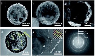 |
| | Fig. 4 Morphological characterization of silicon micron cages (SMCs). (a and b) The magnified SEM image of (SMC); (c) the inner surface of SMC. (d) TEM image of SMC (the yellow dash lines represent the slits in the SMC); (e) HRTEM image of SMC (amorphous SiO2 covering the surface of SMC indicating the oxidation of Si when exposure to air; the inset image magnified of the white box showing the crystalline structure of SMC); (f) the SAED pattern of SMC. | |
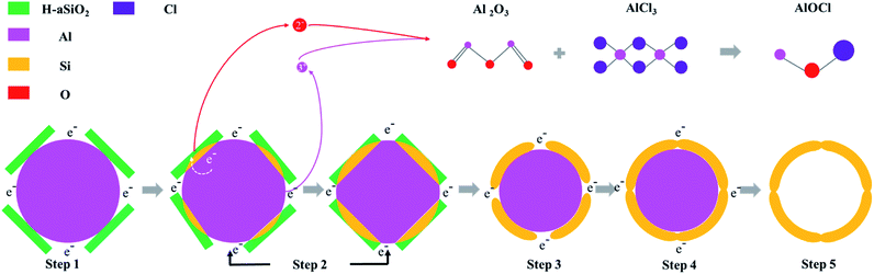
COM-Si was synthesized using aluminum with larger particle diameter (100–200 μm) as reductant through the same process. The SEM image of COM-Si shows irregular bulk (Fig. 5a), which is different from SMCs, confirming the sacrificial template role of spherical aluminum in preparing SMCs. First, previous reports introduced that ionization process (Al = Al3+ + 3e−) may exist in molten AlCl3 during the reduction process.15 The tubular Si material is expected to be obtained for the tubular morphology of H-aSiO2. However, the Si material synthesized in this work shows the morphology of the silicon micron cage, which is different from H-aSiO2 in both size and shape. Therefore, the electrons provided by the ionization process of Al are distributed near the surface of the Al particles. Consequently, the reduction process in this study takes place near the surface of the Al particles. Second, the tubular morphology of unreduced H-aSiO2 shows the undecomposable of H-aSiO2 in the molten salt (Fig. 5b). Only when attached to or near the aluminum sphere dose the reduction of H-aSiO2 take place. The tubular H-aSiO2 was reformed into silicon branches and then attached to the aluminum sphere. Since the SMCs are composed of silicon branches that are not present in COM-Si, the nano aluminum sphere is considered to facilitate the formation of silicon branches. Finally, the magnified image of an incomplete SMC shows a tendency of silicon branches to connect together if they grow further (Fig. 5c). Based on the above analysis, the formation mechanism of SMCs was proposed in a brief illustration (Fig. 6). Step 1, liquid phase molten AlCl3 ensures the tight contact of reactants and avoids the appearance of Al2O3 passivation layer.16 Step 2, the reduction process begins at the contact point of the reactants first. Step 3, silicon branches grow as more H-aSiO2 is reduced to silicon. Step 4, as the reduction progresses, the silicon branches are connected to form a silicon micron cage. Step 5, SMC will be obtained after aluminum is eliminated with HCl solution.
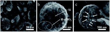 |
| | Fig. 5 SEM images of (a) Silicon material prepared using aluminum with larger particle diameter of 100–200 μm as reductant by the same method as SMCs, (b) the magnified image of prepared SMCs crud products after HCl washing and (c) the incomplete SMC shows the growth trend of silicon branches. | |
 |
| | Fig. 6 Schematic illustration of the formation mechanism of silicon micron cages (SMCs). | |
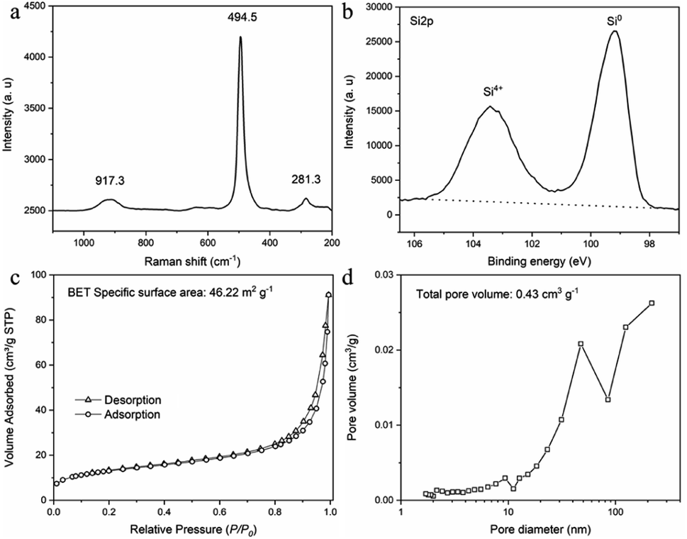
Raman test was conducted to confirm the composition of SMCs (Fig. 7a). One sharp peak at 494.5 cm−1 (resulting from the Si–Si stretching mode) and two weak and broad peaks at 281.3 cm−1 and 917.3 cm−1 (corresponding to the overtones of TA(X) and TO(L),7 respectively) were detected. The location of all three peaks moved to lower Raman shift for approximately 20 cm−1, attributing to the small size of the prepared silicon particles.17 The surface content of prepared SMCs was tested by X-ray photo-electron spectroscopy (XPS) spectrum (Fig. 7b). The high resolution Si 2p XPS spectrum of SMCs shows a strong peak at 99.12 eV and a relatively weak peak at 103.4 eV, corresponding to Si0 and Si4+, respectively.18 The peak of Si4+ suggests the oxidation of silicon when exposed to air.19 The nitrogen adsorption–desorption isotherms and pore size distribution curve of SMCs are presented in (Fig. 7c and d). A type of IV isotherm and H3 hysteresis loops was observed, indicating mesoporous structure. The rapid increase in the N2 adsorption capacity in the high relative pressure region indicated the existence of macropores.7 The specific surface area and total pore volume are 46.22 m2 g−1 and 0.134 cm3 g−1 analyzed by Brunauer–Emmett–Teller (BET) and Barrett–Joyner–Halenda (BJH) measurements, respectively. The pore size distribution curve shows a peak located at around 50 nm, and rises continually when the pore size is larger than 100 nm, indicating the pore size is mainly mesoporous and macropore.
 |
| | Fig. 7 Characterization of silicon micron cages (SMCs). (a) Raman spectrum; (b) XPS spectrum; (c) nitrogen adsorption–desorption isotherm; (d) pore size distribution curve. | |
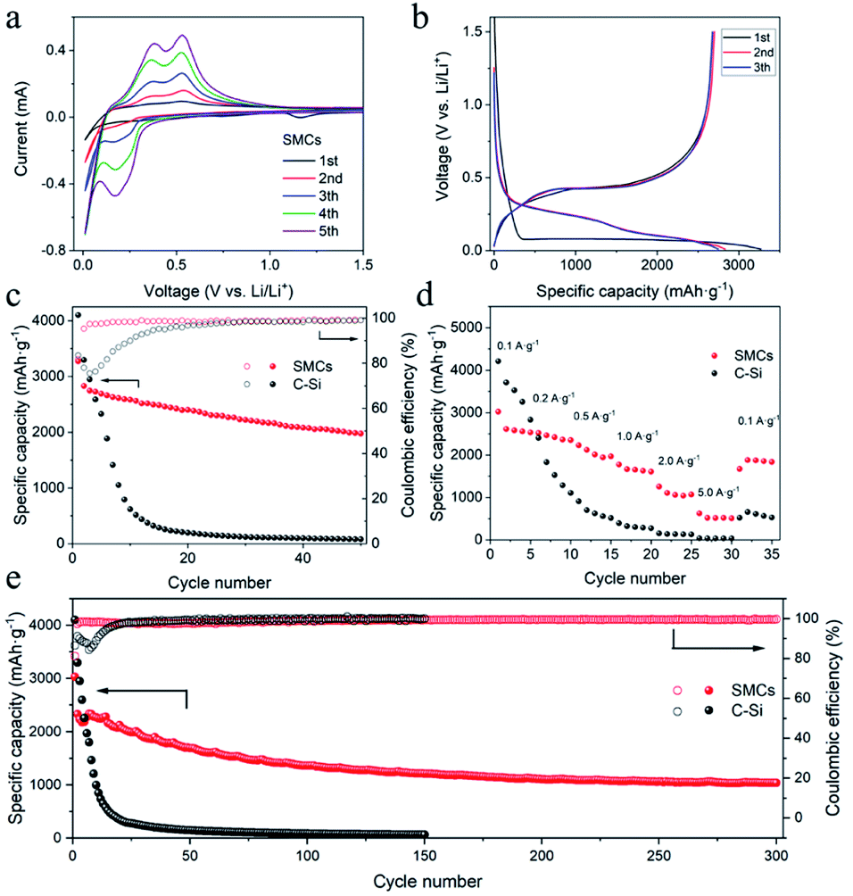
Half-cell lithium-ion battery performance was investigated by applying SMCs and commercial silicon (C–Si) as anode electrode material. Cyclic voltammetry (CV) test was conducted at 0.1 mV s−1 to investigate the lithiation/delithiation process of SMCs (Fig. 8a). In the initial cathodic process, a weak peak at about 1.16 V is corresponding to the formation of SEI film at the surface of silicon.10 A strong peak at around 0.01 V could be assigned to the formation of the amorphous-Li15Si4 phase and followed by the cubic Li15Si4 phase.8 In the anodic scan, two peaks at 0.38 and 0.53 V can be attributed to the delithiation of LixSi alloys to amorphous-Si. After the first cycle, a new peak near 0.17 V appeared, which is associated with the lithiation process and finally results in the reversible transformation from amorphous Si to LixSi alloy. The current of CV peaks increased gradually, indicating the activation of crystalline Si, which is similar to previous reports.20,21 The galvanostatic charge/discharge of SMCs tested at 0.2 A g−1 for the 1st, 2nd and 3rd cycles are plotted in Fig. 8b. The cells were deep charged and discharged between 0.005 V and 1.5 V, and the plateau of charge–discharge curves is consistent well with the CV curve, respectively. In the initial cycle, the main potential plateau of the discharge process was located at around 0.1 V, agreeing well with the lithiation process of crystalline Si. In the following cycles, the main discharge potential plateau shows around 0.1–0.5 V, which is attributed to the transformation from amorphous Si to LixSi alloy. The initial discharge and charge capacities were 3272.8 and 2675.9 mA h g−1 for SMCs, respectively, which was lower than 4102.7 and 3548.6 mA h g−1 for C–Si. The initial coulombic efficiency (CE) of SMCs was 81.8%, which was lower than 83.6% for C–Si. The lower CE of SMCs could be attributed to the larger specific surface area of SMCs since the micron cage structure, resulting in more SEI film formation. The 2nd cycle coulombic efficiency increased to 95.3%, and the average coulombic efficiency for the cycles from 3 to 50 is 98.6%, suggesting the excellent reversibility of SMCs electrode. SMCs shows a slow capacity decay from 3272.8 mA h g−1 to a reversible capacity of 1977.5 mA h g−1 after 50 cycles at a current density of 0.2 A g−1, while the reversible capacity of C–Si decayed seriously from 4102.7 mA h g−1 to 81.2 mA h g−1 after 50 cycles (Fig. 8c).
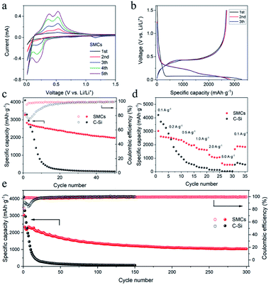 |
| | Fig. 8 Electrochemical performance of silicon micron cages (SMCs) and commercial silicon (C–Si). (a) Cyclic voltammograms of first five cycles of SMCs at a scan rate of 0.1 mV s−1; (b) discharge–charge voltage curves at current density of 0.2 A g−1; (c) cycling stability at 0.2 A g−1 for SMCs and C–Si; (d) rate performance of SMCs and C–Si; (e) long-term cycling of SMCs and C–Si at 1 A g−1. | |
Rate performances of SMCs and C–Si were evaluated using galvanostatic charge–discharge measurements by increasing the current density from a low value of 0.1 to 5.0 A g−1 and then back to 0.1 A g−1 (Fig. 8d). The stable discharge capacities of SMCs electrode were 2573.5, 2401.4, 2013.1, 1640.9, 1070.4 and 515.9 mA h g−1 at current densities of 0.1, 0.2, 0.5, 1.0, 2.0 and 5.0 A g−1, respectively. When current density increased from 0.1 to 5.0 A g−1, 20% reversible capacity has been maintained for SMCs, significantly improved than C–Si (1.1%). Besides, while the current density returns to 0.1 A g−1, the reversible capacity of SMCs can immediately recover to 1881.8 mA h g−1, suggesting excellent rate capability. A discharge specific capacity of 1035.1 mA h g−1 after 300 cycles for SMCs electrode at a higher current density of 1.0 A g−1 was attained, which is higher than the values from the most recent reports6–9,11,15,22–24 (for detailed data, see Table S1†). Compared with the third cycle, the capacity retention of the 300th cycle is 46.4%. Some oscillations in the specific capacity values could be observed in the first 100 cycles. This may result from the temperature difference, the active sites, and the surface conditions of the sample and the SEI layer thickness.18,25 In contrast, the capacity of C–Si electrode drops rapidly from 4102.7 mA h g−1 to 60.8 mA h g−1 in 150 cycles (Fig. 8e).
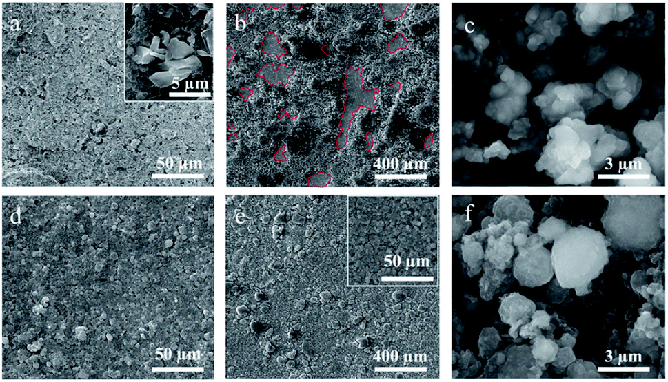
The top-view and cross-sectional images of silicon micron cages (SMCs) and commercial silicon (C–Si) electrodes before and after cycling were obtained using SEM to further investigate the volume expansion and long-term structural stability. The inset image in (Fig. 9a) shows the irregular particle morphology of C–Si with similar diameter to SMCs. Compared to that of the pristine C–Si electrode (Fig. 9a), the electrode collapsed severely after 50 cycles (Fig. 9b) due to the volume change of C–Si during cycling. Fortunately, the SMCs electrode (Fig. 9d) shown relatively neat surface morphology with tiny cracks after 50 cycles compared to the pristine electrode (Fig. 9e). The C–Si particles have been destroyed after cycling (Fig. 9c), while no severe crack or fracture of SMCs were found (Fig. 9f), which indicates the excellent cyclic stability of SMCs. The cross-sectional image of C–Si (Fig. 10a) and SMCs (Fig. 10c) electrodes shows that the active material binds tightly to the copper foil collector. After 50 cycles, part of the active material of C–Si electrode is detached from the collector (Fig. 10b), while the SMCs active material still binds tightly to the collector (Fig. 10d), showing outstanding structural stability of SMCs electrode during long cycling. The improved electrochemical performance and structural stability of SMCs electrode can be attributed to the micron cage constructed through using spherical aluminum particles as sacrificial template. Abundant buffering space and mesopores provided by the micron cage structure ease the Si expansion and promote the fast ion immigration during the charge and discharge process.3,26
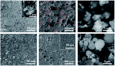 |
| | Fig. 9 SEM images of the microscopic morphological changes of commercial silicon (C–Si) and silicon micron cages (SMCs) electrode in the long cycling process at 1 A g−1. (a and b) Top-view images of C–Si electrode before cycling and after 50 cycles (the inset shows the irregular particle morphology of C–Si with similar diameter to SMCs); (c) the morphology characterization of C–Si particles after 50 cycles; (d and e) top-view images of SMCs electrode before cycling and after 50 cycles; (f) the morphology characterization of SMCs after 50 cycles. | |
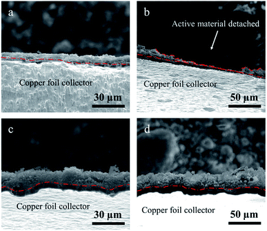 |
| | Fig. 10 Cross-sectional SEM images of (a and b) commercial silicon (C–Si) and (c and d) silicon micron cages (SMCs) electrodes before and after 50 cycles at 1 A g−1. | |
Conclusions
Silicon micron cages (SMCs) have been successfully synthesized in molten AlCl3 through using spherical aluminum particles as sacrificial template, and the earth-abundant and low-cost of natural halloysite clay as precursor. The aluminum spheres (1–3 μm) not only act as a sacrificial template but also facilitate the formation of silicon branches, which connect together to form SMCs. As anodes for lithium-ion batteries, SMCs exhibited a high reversible capacity of 1977.5 mA h g−1 after 50 cycles at a current density of 0.2 A g−1, and 1035.1 mA h g−1 after 300 cycles at a current density of 1.0 A g−1. The improved electrochemical performance of SMCs could be attributed to the micron cage structure. Abundant buffering space and mesopores provided by the micron cage structure ease the Si expansion and promote the fast ion immigration during the charge and discharge process. This promising method is expected to offer a pathway towards the scalable application of Si-base anode materials in the next-generation LIB technology.
Author contributions
Bo Li: conceptualization, methodology, validation, data curation, formal analysis, software, visualization, writing – original draft, writing – review & editing. Xiuyun Chuan: funding acquisition, project administration, supervision, resources, reviewing and editing. Shunpeng Chen: methodology, review & editing. Fangfang Liu: methodology, formal analysis, reviewing and editing. Xingguo Li: project administration, resources, methodology.
Conflicts of interest
The authors declare no conflicts of interest.
Acknowledgements
This study was financially supported by the National Natural Science Foundation of China (Grant No. 52074015 and 51774016) and the Test Fund of Peking University (0000012321).
Notes and references
- B. Bang, J. I. Lee, H. Kim, J. Cho and S. Park, Adv. Energy Mater., 2012, 2, 878–883 CrossRef CAS.
- M. H. Park, M. G. Kim, J. Choo, K. Kim, J. Kim, S. Ahn, Y. Cui and J. Cho, Nano Lett., 2009, 9, 3844–3847 CrossRef CAS PubMed.
- Y. Yao, M. McDowell, I. Ryu, H. Wu, N. Liu, L. Hu, W. D. Nix and Y. Cui, Nano Lett., 2011, 11, 2949–2954 CrossRef CAS PubMed.
- Z. Lu, J. Zhu, D. Sim, W. Zhou, W. Shi, H. H. Hng and Q. Yan, Chem. Mater., 2011, 23, 5293–5295 CrossRef CAS.
- S. Chen, X. Wu, Z. Liu, B. Sun, J. Deng, H. Zeng, C. Xinghua, J. Zheng and X. Li, J. Solid State Chem., 2021, 302, 122408 CrossRef CAS.
- X. Huang, D. Cen, R. Wei, H. Fan and Z. Bao, ACS Appl. Mater. Interfaces, 2019, 11, 26854–26862 CrossRef CAS PubMed.
- Q. Chen, R. Zhu, S. Liu, D. Wu and H. He, J. Mater. Chem. A, 2018, 6, 6356–6362 RSC.
- Y. Zhang, R. Zhang, S. Chen, H. Gao, M. Li, X. Song, H. Xin and Z. Chen, Adv. Funct. Mater., 2020, 30, 2005956 CrossRef CAS.
- X. Zhou, L. Wu, J. Yang, J. Tang, L. Xi and B. Wang, J. Power Sources, 2016, 324, 33–40 CrossRef CAS.
- W. Tang, X. X. Guo, X. H. Liu, G. Chen, H. J. Wang, N. Zhang, J. Wang, G. Z. Qiu and R. Z. Ma, Appl. Clay Sci., 2018, 162, 499–506 CrossRef CAS.
- H. Wan, H. Xiong, X. Liu, G. Chen, N. Zhang, H. Wang, R. Ma and G. Qiu, Dalton Trans., 2018, 47, 7522–7527 RSC.
- G. P. Zhou, Acta Mineral. Sin., 1990, 10(1), 46–52 Search PubMed.
- E. Joussein, S. Petit, J. Churchman, B. Theng, D. Righi and B. Delvaux, Clay Miner., 2005, 40, 383–426 CrossRef CAS.
- E. Abdullayev, A. Joshi, W. Wei, Y. Zhao and Y. Lvov, ACS Nano, 2012, 6, 7216–7226 CrossRef CAS PubMed.
- N. Lin, Y. Han, J. Zhou, K. Zhang, T. Xu, Y. Zhu and Y. Zhou, Energy Environ. Sci., 2015, 8, 3187–3191 RSC.
- L. Wang, Z. Munir and Y. Maximov, J. Mater. Sci., 1993, 28, 3693–3708 CrossRef CAS.
- L. B. Wang, N. Lin, J. B. Zhou, Y. C. Zhu and Y. T. Qian, Chem. Commun., 2015, 51, 2345–2348 RSC.
- X. Li, Y. Zhu, C. Guo and Y. Qian, Nano Res., 2014, 8(5), 1497–1504 Search PubMed.
- H. Kim, M. Seo, M.-H. Park and J. Cho, Angew. Chem., 2010, 49, 2146–2149 CrossRef CAS PubMed.
- X. Ding, X. Liu, Y. Huang, X. Zhang, Q. Zhao, X. Xinghua, G. Li, P. He, Z. Wen, J. Li and Y. Huang, Nano Energy, 2016, 27, 647–657 CrossRef CAS.
- P. Li, J. Y. Hwang and Y. K. Sun, ACS Nano, 2019, 13, 2624–2633 CAS.
- C. Fang, J. Liu, X. Zhang, W. Luo, X. Li, Z. Liu, P. Yin and W. Feng, ACS Appl. Mater. Interfaces, 2021, 13, 29726–29736 CrossRef CAS PubMed.
- W. Li, J. Peng, H. Li, Z. Wu, Y. Huang, B. Chang, X. Guo, G. Chen and X. Wang, ACS Appl. Energy Mater., 2021, 4, 8529–8537 CrossRef CAS.
- J. Peng, W. Li, Z. Wu, H. Li, P. Zeng, G. Chen, B. Chang, X. Zhang and X. Wang, Sustainable Mater. Technol., 2022, 32, e00410 CrossRef CAS.
- J. H. Cho and S. Picraux, Nano Lett., 2014, 14, 3088–3095 CrossRef CAS PubMed.
- M. Ge, J. Rong, X. Fang, A. Zhang, Y. Lu and C. Zhou, Nano Res., 2013, 6, 174–181 CrossRef CAS.
|
| This journal is © The Royal Society of Chemistry 2022 |
Click here to see how this site uses Cookies. View our privacy policy here. 
 Open Access Article
 This Open Access Article is licensed under a Creative Commons Attribution-Non Commercial 3.0 Unported Licence
 a,
Xiuyun Chuan‡*a,
Shunpeng Chen‡b,
Fangfang Liu
a,
Xiuyun Chuan‡*a,
Shunpeng Chen‡b,
Fangfang Liu